Chapters
Table of Contents

Related Manuals for IEI Technology WAFER-945GSE


Summary of Contents for IEI Technology WAFER-945GSE
- Page 1 WAFER-945GSE 3.5” Motherboard WAFER-945GSE 3.5” Motherboard WAFER-945GSE 3.5" SBC with Intel® Atom™ Processor with support for VGA and LVDS Displays, Dual PCIe GbE, CF Type II, and SATA Page i Rev. 1.03 - 26 May, 2009...
- Page 2 WAFER-945GSE 3.5” Motherboard Revision Date Version Changes 26 May, 2009 1.03 Modified LVDS connector description in Section 4.3.10 12 March, 2009 1.02 Changed model name 8 January, 2009 1.01 Added a warning for using heat sink enclosure on page 92 4 November, 2008 1.00...
- Page 3 WAFER-945GSE 3.5” Motherboard Copyright COPYRIGHT NOTICE The information in this document is subject to change without prior notice in order to improve reliability, design and function and does not represent a commitment on the part of the manufacturer. In no event will the manufacturer be liable for direct, indirect, special, incidental, or consequential damages arising out of the use or inability to use the product or documentation, even if advised of the possibility of such damages.
- Page 4 Cautionary messages should also be heeded to help reduce the chance of losing data or damaging the WAFER-945GSE. Cautions are easy to recognize. The word “caution” is written as “CAUTION,” both capitalized and bold and is followed. The italicized text is the cautionary message.
- Page 5 “NOTE,” both capitalized and bold and is followed by text. The text is the cautionary message. A note message is shown below: NOTE: This is an example of a note message. Notes should always be read. Notes contain critical information about the WAFER-945GSE. Please take note messages seriously. Page v...
- Page 6 To contact an IEI sales representative, please send an email to s ales@iei.com.tw. The items listed below should all be included in the WAFER-945GSE package. 1 x WAFER-945GSE Single Board Computer 1 x 4-port RS-232 cable (P/N: 32200-025401-RS)
-
Page 7: Table Of Contents
..................VERVIEW 4 0 1 H 1 .2.1 WAFER-945GSE Overview Photo ..............4 0 2 H 1 .2.2 WAFER-945GSE Peripheral Connectors and Jumpers........4 0 3 H 1 .2.3 Technical Specifications..................4 0 4 H DETAILED SPECIFICATIONS ................4 0 5 H 2 .1 D... - Page 8 WAFER-945GSE 3.5” Motherboard ® 2 .5.6 Intel ICH7-M SATA Controller ..............3 1 H 4 2 8 H ® 2 .5.7 Intel ICH7-M USB Controller................ 3 2 H 4 2 9 H 2 .6 LPC B ................... OMPONENTS 3 3 H 4 3 0 H 2 .6.1 LPC Bus Overview...................
- Page 9 WAFER-945GSE 3.5” Motherboard 4 .3.4 Backlight Inverter Connector ................6 4 H 4 6 1 H 4 .3.5 CompactFlash® Socket..................6 5 H 4 6 2 H 4 .3.6 Digital Input/Output (DIO) Connector............6 6 H 4 6 3 H 4 .3.7 Fan Connector (+12V, 3-pin) ................
- Page 10 WAFER-945GSE 3.5” Motherboard 5 .5.6 LVDS Voltage Selection..................9 8 H 4 9 5 H 5 .6 C .................... HASSIS NSTALLATION 9 9 H 4 9 6 H 5 .6.1 Airflow......................1 0 0 H 4 9 7 H 5 .6.2 Motherboard Installation.................
- Page 11 WAFER-945GSE 3.5” Motherboard 6 .3.5.1 ACPI configuration .................. 1 16 1 3 2 H 5 2 9 H 6 .3.5.2 APM Configuration.................. 1 17 1 3 3 H 5 3 0 H 6 .3.6 Remote Configuration ..................1 20 1 3 4 H 5 3 1 H 6 .3.7 USB Configuration..................
- Page 12 WAFER-945GSE 3.5” Motherboard E .3 M ..................1 79 EMORY DDRESS 1 6 4 H 5 6 1 H HAZARDOUS MATERIALS DISCLOSURE ........... 1 80 1 6 5 H 5 6 2 H F .1 H IPB P AZARDOUS ATERIAL...
- Page 13 List of Figures F igure 1-1: WAFER-945GSE..................1 6 7 H 5 6 4 H F igure 1-2: WAFER-945GSE Overview [Front View]..........1 6 8 H 5 6 5 H F igure 2-1: WAFER-945GSE Dimensions (mm) ............1 6 9 H 5 6 6 H F igure 2-2: External Interface Panel Dimensions (mm)..........
- Page 14 5 9 7 H F igure 4-18: USB Connector Pinout Locations............2 0 1 H 5 9 8 H F igure 4-19: WAFER-945GSE External Peripheral Interface Connector....2 0 2 H 5 9 9 H F igure 4-20: RJ-45 Ethernet Connector ..............
- Page 15 WAFER-945GSE 3.5” Motherboard F igure 5-22: VGA Connector ..................2 2 7 H 6 2 4 H F igure 5-23: Heat Sink Retention Screws ..............2 2 8 H 6 2 5 H F igure 7-1: Start Up Screen..................1 43...
- Page 16 WAFER-945GSE 3.5” Motherboard List of Tables T able 1-1: Technical Specifications ................2 5 5 H 6 5 2 H T able 2-1: Power Consumption ................. 2 5 6 H 6 5 3 H T able 4-1: Peripheral Interface Connectors..............
- Page 17 WAFER-945GSE 3.5” Motherboard T able 5-3: CF Card Setup Jumper Settings .............. 2 8 3 H 6 8 0 H T able 5-4: Clear CMOS Jumper Settings ..............2 8 4 H 6 8 1 H T able 5-5: COM 2 Function Select Jumper Settings..........
- Page 18 WAFER-945GSE 3.5” Motherboard List of BIOS Menus M enu 1: Main........................ 2 9 0 H 6 8 7 H M enu 2: Advanced....................... 2 9 1 H 6 8 8 H M enu 3: CPU Configuration ..................1 00 2 9 2 H 6 8 9 H M enu 4: IDE Configuration ..................
- Page 19 WAFER-945GSE 3.5” Motherboard THIS PAGE IS INTENTIONALLY LEFT BLANK Page xix...
-
Page 21: Introduction
WAFER-945GSE 3.5” Motherboard Chapter Introduction Page 1... -
Page 22: Overview
The Intel® Atom™ processor N270 embedded on the WAFER-945GSE has a 1.60 GHz clock speed, a 533 MHz FSB and a 512 KB L2 cache. The WAFER-945GSE also supports one 200-pin 533 MHz 2.0 GB (max.) DDR2 SDRAM SO-DIMM. The board comes with an LVDS connector and supports both 18-bit and 36-bit single channel LVDS screens. -
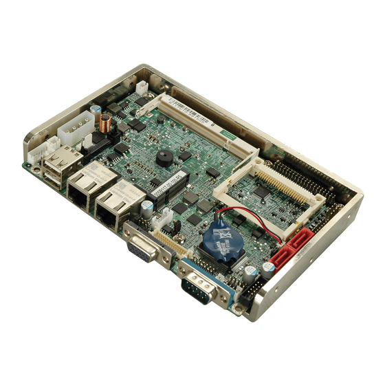
Page 23: Wafer-945Gse Peripheral Connectors And Jumpers
WAFER-945GSE 3.5” Motherboard Figure 1-2: WAFER-945GSE Overview [Front View] 1.2.2 WAFER-945GSE Peripheral Connectors and Jumpers The WAFER-945GSE has the following connectors on-board: 1 x ATX power connector 1 x ATX enable connector 1 x Audio connector 1 x Backlight inverter connector 1 x CompactFlash®... -
Page 24: Technical Specifications
1 x RS-232/422/485 serial port connector 2 x Serial ATA (SATA) drive connectors 2 x USB 2.0 connectors (supports four USB 2.0 devices) The WAFER-945GSE has the following external peripheral interface connectors on the board rear panel. 2 x Ethernet connectors... - Page 25 WAFER-945GSE 3.5” Motherboard Northbridge: Intel® 945GSE System Chipset Southbridge: Intel® ICH7-M One 200-pin SO-DIMM socket supports one 400 MHz or Memory 533 MHz 2.0 GB (max.) DDR2 SDRAM SO-DIMM CompactFlash® One CompactFlash® Type II socket Super I/O ITE IT8718 Intel® Generation 3.5 integrated GFX core (133 MHz) Display 18-bit dual channel LVDS integrated in Intel®...
-
Page 26: Table 1-1: Technical Specifications
WAFER-945GSE 3.5” Motherboard 5.0 V only Power Supply 12 V for LCD/System Fan AT and ATX support 5V @ 2.94 A Power Consumption 1.6 GHz Intel® Atom™ with one 1.0 GB DDR2 SO-DIMM Temperature 0ºC – 60ºC (32ºF - 140ºF) -
Page 27: Detailed Specifications
WAFER-945GSE 3.5” Motherboard Chapter Detailed Specifications Page 7... -
Page 28: Dimensions
WAFER-945GSE 3.5” Motherboard 2.1 Dimensions 2.1.1 Board Dimensions The dimensions of the board are shown below: Page 8... -
Page 29: External Interface Panel Dimensions
WAFER-945GSE 3.5” Motherboard Figure 2-1: WAFER-945GSE Dimensions (mm) 2.1.2 External Interface Panel Dimensions External peripheral interface connector panel dimensions are shown in F igure 2-2. 7 4 8 H 7 1 0 H Figure 2-2: External Interface Panel Dimensions (mm) 2.2 Data Flow... -
Page 30: Embedded Wafer-945Gse Processor
Figure 2-3: Data Flow Block Diagram 2.3 Embedded WAFER-945GSE Processor 2.3.1 Overview The WAFER-945GSE comes with an embedded 45 nm 1.60 GHz Intel® Atom™ processor N270. The processor supports a 533 MHz FSB and has a 1.6 GHz 512 KB L2 Page 10... -
Page 31: Features
WAFER-945GSE 3.5” Motherboard cache. The low power processor has a maximum power of 2.5 W. The processor is covered with a heat sink and is shown in F igure 2-4 below. 7 1 2 H Figure 2-4: Embedded Processor 2.3.2 Features Some of the features of the Intel®... -
Page 32: Figure 2-5: Front Side Bus
Execute Disable Bit support for enhanced security 2.3.3 Front Side Bus (FSB) The Intel® Atom™ processor on the WAFER-945GSE is interfaced to the Intel 945GSE Northbridge through a 533 MHz front side bus (FSB). The FSB is shown in F igure 2-5 7 5 2 H 7 1 3 H below. -
Page 33: Intel 945Gse Northbridge Chipset
Intel® Atom™ N270 processor. The Intel 945GSE is interfaced to the processor through a 533 MHz FSB. 2.4.2 Intel® 945GSE DDR2 Controller There is one 200-pin DDR2 SO-DIMM socket on the WAFER-945GSE. The socket supports DDR2 SO-DIMM with the following specifications: Maximum Memory supported 2 GB (1 GB per rank) -
Page 34: Intel® 945Gse Graphics
WAFER-945GSE 3.5” Motherboard Figure 2-6: DDR2 SO-DIMM Socket 2.4.3 Intel® 945GSE Graphics The Intel® 945GSE supports CRT and LVDS. The internal graphics engine has the following features: Intel® Gen 3.5 Integrated Graphics Engine 250-MHz core render clock and 200 MHz core display clock at 1.05-V core... -
Page 35: Analog Crt Graphics Mode
WAFER-945GSE 3.5” Motherboard 4x pixel rate HWMC Microsoft DirectX* 9.1 operating system Intermediate Z in Classic Rendering Internal Graphics Display Device States: D0, D1, D3 Graphics Display Adapter States: D0, D3. 2.4.3.1 Analog CRT Graphics Mode The analog CRT bus is interfaced to an external DB-15 interface connector. The connector is shown below. -
Page 36: Lvds Interface
WAFER-945GSE 3.5” Motherboard Support for CRT Hot Plug 2.4.3.2 LVDS Interface The LVDS interface is connected directly to one of the LVDS connectors on the board. Figure 2-8: LVDS Connector Some of the features of the LVDS interface include: Panel support up to UXGA (1600 x 1200) 25-MHz to 112-MHz single-/dual-channel;... -
Page 37: Intel ® Ich7-M Southbridge Chipset
WAFER-945GSE 3.5” Motherboard ® 2.5 Intel ICH7-M Southbridge Chipset ® 2.5.1 Intel ICH7-M Overview The Intel® ICH7-M southbridge chipset is connected to the Intel® 945GSE northbridge GMCH through the chip-to-chip Direct Media Interface (DMI). Figure 2-9: Direct Media Interface Some of the features of the Intel® ICH7-M are listed below. -
Page 38: Intel ® Ich7-M Audio Codec '97 Controller
Integrated SATA host controller with DMA operations interfaced to four SATA connectors on the WAFER-945GSE Integrated IDE controller supports Ultra ATA 100/66/33 Supports the four USB 2.0 devices on the WAFER-945GSE with four UHCI controllers and one EHCI controller Complies with System Management Bus (SMBus) Specification, Version 2.0 Supports Audio Codec ’97 (AC’97) Revision 2.3... - Page 39 WAFER-945GSE 3.5” Motherboard Meets performance requirements for audio on PC99/2001 systems Meets Microsoft WHQL/WLP 2.0 audio requirements 16-bit Stereo full-duplex CODEC with 48KHz sampling rate Compliant with AC'97 Rev 2.3 specifications Front-Out, Surround-Out, MIC-In and LINE-In Jack Sensing 14.318MHz -> 24.576MHz PLL to eliminate crystal 12.288MHz BITCLK input...
-
Page 40: Intel ® Ich7-M Low Pin Count (Lpc) Interface
WAFER-945GSE 3.5” Motherboard ® 2.5.3 Intel ICH7-M Low Pin Count (LPC) Interface The ICH7-M LPC interface complies with the LPC 1.1 specifications. The LPC bus from the ICH6 is connected to the following components: BIOS chipset Super I/O chipset ®... -
Page 41: Figure 2-11: Realtek Rtl8111C Pcie Gbe Controllers
WAFER-945GSE 3.5” Motherboard Figure 2-11: Realtek RTL8111C PCIe GbE Controllers The Realtek RTL8111C PCIe GbE controllers combine a triple-speed IEEE 802.3 compliant Media Access Controller (MAC) with a triple-speed Ethernet transceiver, 32-bit PCIe bus controller, and embedded memory. With state-of-the-art DSP technology and mixed-mode signal technology, they offer high-speed transmission over CAT 5 UTP cable or CAT 3 UTP (10Mbps only) cable. -
Page 42: Pcie Mini Expansion Slot
WAFER-945GSE 3.5” Motherboard Auto-Negotiation with Next Page capability Supports PCI Express™ 1.1 Supports pair swap/polarity/skew correction Crossover Detection & & Auto-Correction Wake-on-LAN and remote wake-up support Microsoft® NDIS5, NDIS6 Checksum Offload (IPv4, IPv6, TCP, UDP) and Segmentation Task-offload (Large send and Giant send) support Supports Full Duplex flow control (IEEE 802.3x) -
Page 43: Intel ® Ich7-M Real Time Clock
The integrated SATA controller on the ICH7-M southbridge supports up to four SATA drives with independent DMA operations. Two SATA controllers are connected to two SATA connectors on the WAFER-945GSE. The SATA connectors are shown in F igure 7 1 8 H 2-13. -
Page 44: Figure 2-13: Sata Connectors
ICH7-M USB Controller Up to six high-speed, full-speed or low-speed USB devices are supported by the ICH7-M on the WAFER-945GSE. High-speed USB 2.0, with data transfers of up to 480MB/s, is enabled with the ICH7-M integrated Enhanced Host Controller Interface (EHCI) compliant host controller. -
Page 45: Figure 2-14: Onboard Usb Implementation
WAFER-945GSE 3.5” Motherboard Figure 2-14: Onboard USB Implementation 2.6 LPC Bus Components 2.6.1 LPC Bus Overview The SIS964 LPC bus is connected to components listed below: BIOS chipset Super I/O chipset LPC Serial Port Chipset 2.6.2 BIOS Chipset The BIOS chipset has a licensed copy of AMI BIOS installed on the chipset. Some of the... -
Page 46: Ite It8718F Super I/O Chipset 2
WAFER-945GSE 3.5” Motherboard Console redirection function support PXE (Pre-boot Execution Environment) support USB booting support 2.6.3 iTE IT8718F Super I/O chipset The iTE IT8718F Super I/O chipset is connected to the ICH7-M southbridge through the LPC bus. Figure 2-15: Super I/O The iTE IT8718F is an LPC interface-based Super I/O device that comes with Environment Controller integration. -
Page 47: Super I/O Lpc Interface 2
WAFER-945GSE 3.5” Motherboard Two 16C550 UARTs for serial port control One IEEE 1284 Parallel Port Keyboard Controller Watchdog Timer Some of the Super I/O features are described in more detail below: 2.6.3.1 Super I/O LPC Interface ® The LPC interface on the Super I/O complies with the Intel Low Pin Count Specification Rev. -
Page 48: Super I/O Fan Speed Controller 2
1 x UART+IR One Watch dog timer with WDTOUT# signal One Frequency input 24/48MHz Powered by 3Vcc 2.7 Environmental and Power Specifications 2.7.1 System Monitoring Two thermal inputs on the WAFER-945GSE Super I/O Enhanced Hardware Monitor monitor the following temperatures: Page 28... -
Page 49: Operating Temperature And Temperature Control 2
WAFER-945GSE 3.5” Motherboard System temperature CPU temperature Eight voltage inputs on the WAFER-945GSE Super I/O Enhanced Hardware Monitor monitor the following voltages: CPU Core +1.05V +3.3V +12V +1.5V +1.8V +5VSB VBAT The WAFER-945GSE Super I/O Enhanced Hardware Monitor also monitors the following... -
Page 50: Table 2-1: Power Consumption
WAFER-945GSE 3.5” Motherboard 2.7.3 Power Consumption T able 2-1 shows the power consumption parameters for the WAFER-945GSE running 7 6 2 H 7 2 0 H with a 1.6 GHz Intel® Atom™ with 1.0 GB DDR2 memory. Voltage Current 2.94A... -
Page 51: Unpacking 3
WAFER-945GSE 3.5” Motherboard Chapter Unpacking Page 31... -
Page 52: A Nti - Static P Recautions 3
WAFER-945GSE and severe injury to the user. Electrostatic discharge (ESD) can cause serious damage to electronic components, including the WAFER-945GSE. Dry climates are especially susceptible to ESD. It is therefore critical that whenever the WAFER-945GSE, or any other electrical component is handled, the following anti-static precautions are strictly adhered to. -
Page 53: U Npacking C Hecklist 3
If any of the components listed in the checklist below are missing, do not proceed with the installation. Contact the IEI reseller or vendor the WAFER-945GSE was purchased from or contact an IEI sales representative directly by sending an email to s ales@iei.com.tw. -
Page 54: Optional Items 3
4 COM (wo bracket) (P/N: 32200-025401-RS) Mini jumper pack (2.0mm) (P/N:33100-000033-RS) Utility CD Quick Installation Guide 3.3.2 Optional Items The WAFER-945GSE is shipped with the following components: Item and Part Number Image Dual USB cable (wo bracket) (P/N: 32000-070300-RS) RS-232/422/485 cable (P/N:32200-026500-RS) -
Page 55: Connectors 3
WAFER-945GSE 3.5” Motherboard Chapter Connectors Page 35... -
Page 56: Figure 4-1: Connector And Jumper Locations [Front Side]
Figure 4-1: Connector and Jumper Locations [Front Side] 4.2 Peripheral Interface Connectors T able 4-1 shows a list of the peripheral interface connectors on the WAFER-945GSE. 7 6 9 H 7 2 7 H Detailed descriptions of these connectors can be found below. -
Page 57: Table 4-1: Peripheral Interface Connectors
USB 2.0 connector Table 4-1: Peripheral Interface Connectors 4.2.1 External Interface Panel Connectors T able 4-2 lists the rear panel connectors on the WAFER-945GSE. Detailed descriptions of 7 7 0 H 7 2 8 H these connectors can be found in Section 4 .4 on page... -
Page 58: Figure 4-2: Atx Power Connector Location
Internal peripheral connectors are found on the motherboard and are only accessible when the motherboard is outside of the chassis. This section has complete descriptions of all the internal, peripheral connectors on the WAFER-945GSE. 4.3.1 ATX Power Connector CN Label:... -
Page 59: Figure 4-3: Atx Power Supply Enable Connector Location
The ATX power supply enable connector enables the WAFER-945GSE to be connected to an ATX power supply. In default mode, the WAFER-945GSE can only us an AT power supply. To enable an ATX power supply the AT Power Select jumper must also be configured. -
Page 60: Figure 4-4: Audio Connector Pinouts (10-Pin)
WAFER-945GSE 3.5” Motherboard PS-ON Table 4-4: ATX Power Supply Enable Connector Pinouts 4.3.3 Audio Connector (10-pin) CN Label: AUDIO1 CN Type: 10-pin header CN Location: F igure 4-4 7 3 5 H CN Pinouts: T able 4-5 7 3 6 H The 10-pin audio connector is connected to external audio devices including speakers and microphones for the input and output of audio signals to and from the system. -
Page 61: Figure 4-5: Panel Backlight Connector Pinout Locations
CN Pinouts: T able 4-6 7 3 8 H The backlight inverter connectors provide the backlights on the LCD display connected to the WAFER-945GSE with +12V of power. Figure 4-5: Panel Backlight Connector Pinout Locations PIN NO. DESCRIPTION LCD Backlight Control... -
Page 62: F Igure 1-1: Wafer-945Gse
WAFER-945GSE 3.5” Motherboard 4.3.5 CompactFlash® Socket CN Label: CN Type: 50-pin header (2x25) CN Location: F igure 4-6 7 3 9 H CN Pinouts: T able 4-7 7 4 0 H A CF Type I or Type II memory card is inserted to the CF socket on the solder side of the WAFER-945GSE. -
Page 63: Table 4-7: Cf Card Socket Pinouts
WAFER-945GSE 3.5” Motherboard PIN NO. DESCRIPTION PIN NO. DESCRIPTION HDC_CS0# HDC_CS1 GROUND GROUND IOR# GROUND IOW# GROUND VCC_COM GROUND IRQ14 VCC_COM VCC_COM GROUND CSEL GROUND GROUND HDD_RESET GROUND IORDY SDREQ SDACK# HDD_ACTIVE# DATA 0 66DET DATA 1 DATA 8 DATA 2... -
Page 64: Figure 4-7: Dio Connector Connector Locations
WAFER-945GSE 3.5” Motherboard Figure 4-7: DIO Connector Connector Locations PIN NO. DESCRIPTION PIN NO. DESCRIPTION Output 3 Output 2 Output 1 Output 0 Input 3 Input 2 Input 1 Input 0 Table 4-8: DIO Connector Connector Pinouts 4.3.7 Fan Connector (+12V, 3-pin) -
Page 65: Figure 4-8: +12V Fan Connector Location
WAFER-945GSE 3.5” Motherboard Figure 4-8: +12V Fan Connector Location PIN NO. DESCRIPTION +12V Fan Speed Detect Table 4-9: +12V Fan Connector Pinouts 4.3.8 Keyboard/Mouse Connector CN Label: KB_MS1 CN Type: 6-pin header (1x6) CN Location: F igure 4-9 7 4 5 H... -
Page 66: Figure 4-9: Keyboard/Mouse Connector Location
WAFER-945GSE 3.5” Motherboard Figure 4-9: Keyboard/Mouse Connector Location PIN NO. DESCRIPTION +5V KB DATA MS DATA MS CLK KB DATA KB CLK GROUND Table 4-10: Keyboard/Mouse Connector Pinouts 4.3.9 LED Connector CN Label: LED_C1 CN Type: 6-pin wafer (1x6) CN Location:... -
Page 67: Figure 4-10: Led Connector Locations
WAFER-945GSE 3.5” Motherboard Figure 4-10: LED Connector Locations PIN NO. DESCRIPTION Power LED+ Power LED- HDD LED+ HDD LED- Table 4-11: LED Connector Pinouts 4.3.10 LVDS LCD Connector LVDS1 CN Label: CN Type: 30-pin crimp (2x10) CN Location: F igure 4-11... -
Page 68: Figure 4-11: Lvds Lcd Connector Pinout Locations
WAFER-945GSE 3.5” Motherboard Figure 4-11: LVDS LCD Connector Pinout Locations PIN NO. DESCRIPTION PIN NO. DESCRIPTION GND1 GND2 A_Y0 A_Y0# A_Y1 A_Y1# A_Y2 A_Y2# A_CK A_CK# GND3 GND4 B_Y0 B_Y0# B_Y1 B_Y1# B_Y2 B_Y2# B_CK B_CK# GND5 GND6 VCC_LCD VCC_LCD... -
Page 69: Figure 4-12: Pcie Mini Card Slot Location
WAFER-945GSE 3.5” Motherboard 4.3.11 PCIe Mini Card Slot CN Label: CN Type: 52-pin Mini PCIe Card Slot CN Location: F igure 4-12 7 9 1 H 7 5 1 H CN Pinouts: T able 4-13 7 5 2 H The PCIe mini card slot enables a PCIe mini card expansion module to be connected to the board. -
Page 70: Table 4-13: Pcie Mini Card Slot Pinouts
WAFER-945GSE 3.5” Motherboard PCIRST# VCC3 PCIRST# PERN2 3VDual PERP2 1.5V SMBCLK PETN2 SMBDATA PETP2 USBD- USBD+ RF_LINK# BLUELED# 1.5V VCC3 Table 4-13: PCIe Mini Card Slot Pinouts Page 50... -
Page 71: Figure 4-13: Power Button Connector Location
WAFER-945GSE 3.5” Motherboard 4.3.12 Power Button Connector CN Label: PWRBTN1 2-pin wafer (1x2) CN Type: CN Location: F igure 4-13 7 5 3 H CN Pinouts: T able 4-14 7 5 4 H The power button connector is connected to a power switch on the system chassis to enable users to turn the system on and off. -
Page 72: Figure 4-14: Reset Button Connector Locations
WAFER-945GSE 3.5” Motherboard The reset button connector is connected to a reset switch on the system chassis to enable users to reboot the system when the system is turned on. Figure 4-14: Reset Button Connector Locations PIN NO. DESCRIPTION Reset Switch Table 4-15: Reset Button Connector Pinouts 4.3.14 SATA Drive Connectors... -
Page 73: Figure 4-15: Sata Drive Connector Locations
WAFER-945GSE 3.5” Motherboard Figure 4-15: SATA Drive Connector Locations PIN NO. DESCRIPTION Table 4-16: SATA Drive Connector Pinouts 4.3.15 Serial Port Connector (COM3, COM4, COM5 and COM6) CN Label: CN Type: 40-pin header (2x20) F igure 4-16 CN Location: 7 5 9 H... -
Page 74: Figure 4-16: Com3 To Com6 Connector Pinout Locations
WAFER-945GSE 3.5” Motherboard COM3 is located on pin 1 to pin 10 COM4 is located on pin 11 to pin 20 COM5 is located on pin 21 to pin 30 COM6 is located on pin 31 to pin 40 Figure 4-16: COM3 to COM6 Connector Pinout Locations PIN NO. -
Page 75: Table 4-17: Com3 To Com6 Connector Pinouts
WAFER-945GSE 3.5” Motherboard PIN NO. DESCRIPTION PIN NO. DESCRIPTION TRANSMIT DATA (TXD5) CLEAR TO SEND (CTS5) DATA TERMINAL READY (DTR5) RING INDICATOR (RI5) DATA CARRIER DETECT (DCD6 DATA SET READY (DSR6) RECEIVE DATA (RXD6) REQUEST TO SEND (RTS6) TRANSMIT DATA (TXD6... -
Page 76: Figure 4-17: Rs-232/422/485 Serial Port Connector Location
WAFER-945GSE 3.5” Motherboard Figure 4-17: RS-232/422/485 Serial Port Connector Location PIN NO. DESCRIPTION PIN NO. DESCRIPTION NDCD NDSR2 NRTS2 NCTS2 NDTR NRI2 TXD485+ TXD485- RXD485+ RXD485- Table 4-18: RS-232/RS-485 Serial Port Connector Pinouts 4.3.17 USB Connectors (Internal) CN Label: USB01 and USB23... -
Page 77: Figure 4-18: Usb Connector Pinout Locations
Table 4-19: USB Port Connector Pinouts 4.4 External Peripheral Interface Connector Panel F igure 4-19 shows the WAFER-945GSE external peripheral interface connector (EPIC) 8 0 3 H 7 6 5 H panel. The WAFER-945GSE EPIC panel consists of the following:... -
Page 78: Figure 4-19: Wafer-945Gse External Peripheral Interface Connector
T able 4-20 8 0 9 H 7 6 7 H The WAFER-945GSE is equipped with two built-in RJ-45 Ethernet controllers. The controllers can connect to the LAN through two RJ-45 LAN connectors. There are two LEDs on the connector indicating the status of LAN. The pin assignments are listed in the... -
Page 79: Figure 4-20: Rj-45 Ethernet Connector
WAFER-945GSE 3.5” Motherboard Figure 4-20: RJ-45 Ethernet Connector The RJ-45 Ethernet connector has two status LEDs, one green and one yellow. The green LED indicates activity on the port and the yellow LED indicates the port is linked. See T able 4-21. -
Page 80: Figure 4-21: Com1 Pinout Locations
8 1 4 H 7 7 2 H CN Pinouts: T able 4-23 8 1 5 H 7 7 3 H The WAFER-945GSE has two external USB 2.0 ports. The ports connect to both USB 2.0 and USB 1.1 devices. Page 60... -
Page 81: F Igure 2-7: Vga Connector
F igure 4-22 and T able 4-24 8 1 7 H 7 7 5 H 8 1 8 H 7 7 6 H The WAFER-945GSE has a single 15-pin female connector for connectivity to standard display devices. Figure 4-22: VGA Connector DESCRIPTION... -
Page 82: Table 4-24: Vga Connector Pinouts
WAFER-945GSE 3.5” Motherboard DESCRIPTION DESCRIPTION HSYNC VSYNC DDCCLK Table 4-24: VGA Connector Pinouts Page 62... -
Page 83: Installation 6
WAFER-945GSE 3.5” Motherboard Chapter Installation Page 63... -
Page 84: A Nti - Static P Recautions 6
WAFER-945GSE and severe injury to the user. Electrostatic discharge (ESD) can cause serious damage to electronic components, including the WAFER-945GSE. Dry climates are especially susceptible to ESD. It is therefore critical that whenever the WAFER-945GSE, or any other electrical component is handled, the following anti-static precautions are strictly adhered to. -
Page 85: I Nstallation C Onsiderations 6
WAFER-945GSE is installed. All installation notices pertaining to the installation of the WAFER-945GSE should be strictly adhered to. Failing to adhere to these precautions may lead to severe damage of the WAFER-945GSE and injury to the person installing the motherboard. 5.2.1 Installation Notices... -
Page 86: Installation Checklist 6
Allow screws to come in contact with the PCB circuit, connector pins, or its components. 5.2.2 Installation Checklist The following checklist is provided to ensure the WAFER-945GSE is properly installed. All the items in the packing list are present A compatible memory module is properly inserted into the slot... -
Page 87: Figure 5-1: So-Dimm Installation
WAFER-945GSE 3.5” Motherboard 5.3 Unpacking When the WAFER-945GSE is unpacked, please check all the unpacking list items listed in Chapter 3 are indeed present. If any of the unpacking list items are not available please contact the WAFER-945GSE vendor reseller/vendor where the WAFER-945GSE was purchased or contact an IEI sales representative. -
Page 88: Cf Card Installation 6
The WAFER-945GSE can support both CF Type I cards and CF Type II cards. For the complete specifications of the supported CF cards please refer to Chapter 2. To install the a CF card (Type 1 or Type 2) onto the WAFER-945GSE, please follow the steps below: Step 1: Locate the CF card socket. -
Page 89: Figure 5-2: Cf Card Installation
OPEN a jumper means removing the Figure 5-3: Jumper Locations plastic clip from a jumper. Before the WAFER-945GSE is installed in the system, the jumpers must be set in accordance with the desired configuration. The jumpers on the WAFER-945GSE are listed in T able 5-1. -
Page 90: Table 5-1: Jumpers
WAFER-945GSE 3.5” Motherboard Description Label Type AT Power Mode Setting ATXCTL1 2-pin header CF Card Setting JCF1 2-pin header Clear CMOS J_CMOS1 3-pin header COM2 Mode Setting 6-pin header LVDS1 Panel Resolution J_LCD_TYPE1 8-pin header LVDS1 Voltage Select J_VLVDS1 3-pin header Table 5-1: Jumpers 5.5.1 AT Power Select Jumper Settings... -
Page 91: Figure 5-4: At Power Select Jumper Location
WAFER-945GSE 3.5” Motherboard AT Power Select Description Short 2 – 3 Use AT power Default Use ATX power Table 5-2: AT Power Select Jumper Settings The location of the AT Power Select jumper is shown in F igure 5-4 below. -
Page 92: Figure 5-5: Cf Card Setup Jumper Location
F igure 5-6 8 3 1 H 7 9 1 H If the WAFER-945GSE fails to boot due to improper BIOS settings, the clear CMOS jumper clears the CMOS data and resets the system BIOS information. To do this, use the jumper cap to close pins 2 and 3 for a few seconds then reinstall the jumper clip back to pins 1 and 2. -
Page 93: Figure 5-6: Clear Cmos Jumper
WAFER-945GSE 3.5” Motherboard AT Power Select Description Short 1 - 2 Keep CMOS Setup Default Short 2 - 3 Clear CMOS Setup Table 5-4: Clear CMOS Jumper Settings The location of the clear CMOS jumper is shown in F igure 5-6 below. -
Page 94: Figure 5-7: Com 2 Function Select Jumper Location
WAFER-945GSE 3.5” Motherboard Short 5-6 RS-485 with RTS Short 7-8 control Table 5-5: COM 2 Function Select Jumper Settings The COM 2 Function Select jumper location is shown in F igure 5-7. 7 9 7 H Figure 5-7: COM 2 Function Select Jumper Location 5.5.5 LVDS1 Panel Resolution Jumper... -
Page 95: Figure 5-8:Lvds Panel Resolution Jumper Pinout Locations
WAFER-945GSE 3.5” Motherboard J_LCD_TYPE1 DESCRIPTION Pin 7- Pin 8 Pin 5- Pin 6 Pin 3- Pin 4 Pin 1-Pin 2 640 x 480 18-bit 800 x 480 18-bit 800 x 600 18-bit (Default) 1024 x 768 18-bit 1280 x 1024 36-bit... -
Page 96: Table 5-7: Lvds Voltage Selection Jumper Settings
WAFER-945GSE 3.5” Motherboard 5.5.6 LVDS Voltage Selection WARNING: Permanent damage to the screen and WAFER-945GSE may occur if the wrong voltage is selected with this jumper. Please refer to the user guide that cam with the monitor to select the correct voltage. -
Page 97: Figure 5-9: Lvds Voltage Selection Jumper Pinout Locations
The WAFER-945GSE must be installed in a chassis with ventilation holes on the sides allowing airflow to travel through the heat sink surface. In a system with an individual power supply unit, the cooling fan of a power supply can also help generate airflow through the board surface. -
Page 98: Table 5-8: Iei Provided Cables
3 2 8 H 3 1 3 H to find out more about the available chassis. 5.6.2 Motherboard Installation To install the WAFER-945GSE motherboard into the chassis please refer to the reference material that came with the chassis. 5.7 Internal Peripheral Device Connections 5.7.1 Peripheral Device Cables... -
Page 99: Figure 5-10: Sata Drive Cable Connection
WAFER-945GSE 3.5” Motherboard 4-COM port kit 5.7.2 SATA Drive Connection The WAFER-945GSE is shipped with two SATA drive cables and one SATA drive power cable. To connect the SATA drives to the connectors, please follow the steps below. Step 1: Locate the connectors. -
Page 100: Figure 5-11: Sata Power Drive Connection
Figure 5-11: SATA Power Drive Connection 5.7.3 Serial Port Connector Cable (Four Ports) Cable Connection The WAFER-945GSE is shipped with one four serial port connector cable. The four serial port connector cable connects four serial port connectors on the cable to the 40-pin serial port connectors on the WAFER-945GSE. -
Page 101: Figure 5-12: Four Serial Port Connector Cable Connection
Step 3: Insert the cable connectors. Once the cable connector is properly aligned with the 40-pin serial port connector on the WAFER-945GSE, connect the cable connector to the on-board connectors. See F igure 5-16. 8 1 1 H Figure 5-12: Four Serial Port Connector Cable Connection Step 4: Attach DB-9 serial port connectors to the chassis. -
Page 102: Figure 5-13: Dual Rs-232 Cable Installation
Step 0: 5.7.5 4-COM Port Adapter Board Connection (Optional) An optional, separately purchased 4-COM port adapter board may be shipped with the WAFER-945GSE. To install the 4-COM Port Adapter Board, please follow the steps below. Step 1: Locate the COM connector. The locations of the COM port connectors are shown in Chapter 4. -
Page 103: Figure 5-14: 4-Com Port Adapter Board
WAFER-945GSE 3.5” Motherboard Step 2: Insert the cable connector. Align the cable connector with the onboard connector. Make sure the pin 1on the cable connector is properly aligned with pin 1 on the board connector. F igure 5-14. 8 1 2 H Step 3: Connect the adapter board to the cable. -
Page 104: Figure 5-15: Serial Device Connector
The WAFER-945GSE is shipped with a keyboard/mouse Y-cable connector. The keyboard/mouse Y-cable connector connects to a keyboard/mouse connector on the WAFER-945GSE and branches into two cables that are each connected to a PS/2 connector, one for a mouse and one for a keyboard. To connect the keyboard/mouse Y-cable connector please follow the steps below. -
Page 105: Figure 5-16: Keyboard/Mouse Y-Cable Connection
PS/2 connector. Step 0: 5.7.7 Audio Kit Installation The Audio Kit that came with the WAFER-945GSE connects to the 10-pin audio connector on the WAFER-945GSE. The audio kit consists of three audio jacks. One audio jack, Mic Page 85... -
Page 106: Figure 5-17: Audio Kit Cable Connection
Step 0: 5.7.8 USB Cable (Dual Port without Bracket) (Optional) The WAFER-945GSE is shipped with a dual port USB 2.0 cable. To connect the USB cable connector, please follow the steps below. Step 1: Locate the connectors. -
Page 107: Figure 5-18: Dual Usb Cable Connection
If the USB pins are not properly aligned, the USB device can burn out. Step 2: Align the connectors. The cable has two connectors. Correctly align pin 1on each cable connector with pin 1 on the WAFER-945GSE USB connector. Step 3: Insert the cable connectors. Once the cable connectors are properly aligned with the USB connectors on the WAFER-945GSE, connect the cable connectors to the on-board connectors. -
Page 108: Figure 5-19: Lan Connection
USB devices VGA monitors To install these devices, connect the corresponding cable connector from the actual device to the corresponding WAFER-945GSE external peripheral interface connector making sure the pins are properly aligned. 5.8.1 LAN Connection (Single Connector) There are two external RJ-45 LAN connectors. The RJ-45 connectors enable connection to an external network. -
Page 109: Figure 5-20: Serial Device Connector
RJ-45 connector into the onboard RJ-45 connector. Step 0: 5.8.2 Serial Device Connection The WAFER-945GSE has a single female DB-9 connector on the external peripheral interface panel for a serial device. Follow the steps below to connect a serial device to the WAFER-945GSE. -
Page 110: Figure 5-21: Usb Connector
WAFER-945GSE 3.5” Motherboard 5.8.3 USB Connection (Dual Connector) The external USB Series "A" receptacle connectors provide easier and quicker access to external USB devices. Follow the steps below to connect USB devices to the WAFER-945GSE. Step 1: Locate the USB Series "A" receptacle connectors. The location of the USB Series "A"... -
Page 111: Vga Monitor Connection 9
WAFER-945GSE 3.5” Motherboard 5.8.4 VGA Monitor Connection The WAFER-945GSE has a single female DB-15 connector on the external peripheral interface panel. The DB-15 connector is connected to a CRT or VGA monitor. To connect a monitor to the WAFER-945GSE, please follow the instructions below. - Page 112 When the WAFER-945GSE is shipped it is secured to a heat sink with five retention screws. If the WAFER-945GSE must be removed from the heat sink, the five retention screws must be removed.
-
Page 113: Figure 5-23: Heat Sink Retention Screws
WAFER-945GSE 3.5” Motherboard Figure 5-23: Heat Sink Retention Screws Page 93... -
Page 114: Bios Screens 9
WAFER-945GSE 3.5” Motherboard Chapter BIOS Screens Page 94... -
Page 115: I Ntroduction 9
WAFER-945GSE 3.5” Motherboard 6.1 Introduction A licensed copy of AMI BIOS is preprogrammed into the ROM BIOS. The BIOS setup program allows users to modify the basic system configuration. This chapter describes how to access the BIOS setup program and the configuration options that may be changed. -
Page 116: Table 6-1: Bios Navigation Keys
WAFER-945GSE 3.5” Motherboard F1 key General help, only for Status Page Setup Menu and Option Page Setup Menu F2 /F3 key Change color from total 16 colors. F2 to select color forward. F10 key Save all the CMOS changes, only for Main Menu Table 6-1: BIOS Navigation Keys 6.1.3 Getting Help... -
Page 117: Main
WAFER-945GSE 3.5” Motherboard 6.2 Main The Main BIOS menu ( B IOS Menu 1) appears when the BIOS Setup program is entered. 8 6 4 H 8 2 3 H The Main menu gives an overview of the basic system information. -
Page 118: Advanced
WAFER-945GSE 3.5” Motherboard Count: The number of CPUs on the motherboard System Memory: Displays the auto-detected system memory. Size: Lists memory size The System Overview field also has two user configurable fields: System Time [xx:xx:xx] Use the System Time option to set the system time. Manually enter the hours, minutes and seconds. -
Page 119: Cpu Configuration 9
WAFER-945GSE 3.5” Motherboard BIOS Menu 2: Advanced 6.3.1 CPU Configuration Use the CPU Configuration menu ( B IOS Menu 3) to view detailed CPU specifications 8 7 3 H 8 3 2 H and configure the CPU. Page 99... -
Page 120: Ide Configuration 1
WAFER-945GSE 3.5” Motherboard BIOS Menu 3: CPU Configuration The CPU Configuration menu ( B IOS Menu 3) lists the following CPU details: 8 7 4 H 8 3 3 H Manufacturer: Lists the name of the CPU manufacturer Brand String: Lists the brand name of the CPU being used... - Page 121 WAFER-945GSE 3.5” Motherboard BIOS Menu 4: IDE Configuration ATA/IDE Configurations [Compatible] Use the ATA/IDE Configurations option to configure the ATA/IDE controller. Disables the on-board ATA/IDE controller. Disabled Compatible Configures the on-board ATA/IDE controller to be in compatible mode. In this mode, a SATA channel will replace one of the IDE channels.
-
Page 122: Ide Master, Ide Slave 1
WAFER-945GSE 3.5” Motherboard Legacy IDE Channels [PATA Pri, SATA Sec] SATA Only Only the SATA drives are enabled. SATA Pri, PATA Sec The IDE drives are enabled on the Primary EFAULT IDE channel. The SATA drives are enabled on the Secondary IDE channel. - Page 123 WAFER-945GSE 3.5” Motherboard BIOS Menu 5: IDE Master and IDE Slave Configuration Auto-Detected Drive Parameters The “grayed-out” items in the left frame are IDE disk drive parameters automatically detected from the firmware of the selected IDE disk drive. The drive parameters are listed as follows: Device: Lists the device type (e.g.
- Page 124 WAFER-945GSE 3.5” Motherboard interrupt if block mode is not used. Block mode allows transfers of up to 64 KB per interrupt. PIO Mode: Indicates the PIO mode of the installed device. Async DMA: Indicates the highest Asynchronous DMA Mode that is supported.
- Page 125 WAFER-945GSE 3.5” Motherboard LBA/Large Mode [Auto] Use the LBA/Large Mode option to disable or enable BIOS to auto detects LBA (Logical Block Addressing). LBA is a method of addressing data on a disk drive. In LBA mode, the maximum drive capacity is 137 GB.
- Page 126 WAFER-945GSE 3.5” Motherboard PIO mode 0 selected with a maximum transfer rate of 3.3MBps PIO mode 1 selected with a maximum transfer rate of 5.2MBps PIO mode 2 selected with a maximum transfer rate of 8.3MBps PIO mode 3 selected with a maximum transfer rate of 11.1MBps PIO mode 4 selected with a maximum transfer rate of 16.6MBps...
- Page 127 WAFER-945GSE 3.5” Motherboard UDMA1 Ultra DMA mode 0 selected with a maximum data transfer rate of 16.6MBps Ultra DMA mode 1 selected with a maximum data transfer UDMA1 rate of 25MBps UDMA2 Ultra DMA mode 2 selected with a maximum data transfer rate of 33.3MBps...
-
Page 128: Super Io Configuration 1
WAFER-945GSE 3.5” Motherboard Disabled Prevents the BIOS from using 32-bit data transfers. Enabled Allows BIOS to use 32-bit data transfers on supported EFAULT hard disk drives. 6.3.3 Super IO Configuration Use the Super IO Configuration menu ( B IOS Menu 6) to set or change the 8 7 8 H 8 3 7 H configurations for the FDD controllers, parallel ports and serial ports. - Page 129 WAFER-945GSE 3.5” Motherboard address is IRQ4 3E8/IRQ4 Serial Port 1 I/O port address is 3E8 and the interrupt address is IRQ4 2E8/IRQ3 Serial Port 1 I/O port address is 2E8 and the interrupt address is IRQ3 Serial Port2 Address [2F8/IRQ3] Use the Serial Port2 Address option to select the Serial Port 2 base address.
- Page 130 WAFER-945GSE 3.5” Motherboard Use the Serial Port3 IRQ option to select the interrupt address for serial port 3. Serial port 3 IRQ address is 10 Serial port 3 IRQ address is 11 EFAULT Serial Port4 Address [2E8] Use the Serial Port4 IRQ option to select the interrupt address for serial port 4.
-
Page 131: Hardware Health Configuration 1
WAFER-945GSE 3.5” Motherboard Serial port 5 I/O port address is 2F0 EFAULT Serial port 5 I/O port address is 2E0 Serial Port5 IRQ [11] Use the Serial Port3 IRQ option to select the interrupt address for serial port 5. Serial port 5 IRQ address is 10... - Page 132 WAFER-945GSE 3.5” Motherboard BIOS Menu 7: Hardware Health Configuration CPU FAN Mode Setting [Full On Mode] Use the CPU FAN Mode Setting option to configure the second fan. Fan is on all the time Full On Mode EFAULT Automatic mode Fan is off when the temperature is low enough.
- Page 133 WAFER-945GSE 3.5” Motherboard CPU Fan Start PWM Slope PWM 1 When the CPU FAN Mode Setting option is in the PWM Manual Mode, the following parameters can be set. CPU Fan PWM control CPU Temp. Limit of OFF [000] WARNING: Setting this value too high may cause the fan to stop when the CPU is at a high temperature and therefore cause the system to be damaged.
- Page 134 WAFER-945GSE 3.5” Motherboard The CPU Temp. Limit of Start option can only be set if the CPU FAN Mode Setting option is set to Automatic Mode. Use the CPU Temp. Limit of Start option to select the CPU temperature at which the cooling fan should automatically turn on. When the fan starts, it rotates using the starting pulse width modulation (PWM) specified in the Fan 3 Start PWM option below.
-
Page 135: Power Configuration 1
WAFER-945GSE 3.5” Motherboard 16 PWM 32 PWM 64 PWM The following system parameters and values are shown. The system parameters that are monitored are: System Temperatures: The following system temperatures are monitored CPU Temperature System Temperature Fan Speeds: The CPU cooling fan speed is monitored. -
Page 136: Acpi Configuration 1
WAFER-945GSE 3.5” Motherboard BIOS Menu 8: Power Configuration 6.3.5.1 ACPI configuration The ACPI Configuration menu ( B IOS Menu 9) configures the Advanced Configuration 8 8 0 H 8 4 0 H and Power Interface (ACPI). Page 116... -
Page 137: Apm Configuration 1
WAFER-945GSE 3.5” Motherboard BIOS Menu 9: ACPI Configuration Suspend Mode [S1(POS)] Use the Suspend Mode BIOS option to specify the sleep state the system enters when it is not being used. S1 (POS) System appears off. The CPU is stopped; RAM is EFAULT refreshed;... - Page 138 WAFER-945GSE 3.5” Motherboard BIOS Menu 10:Advanced Power Management Configuration Restore on AC Power Loss [Last State] Use the Restore on AC Power Loss BIOS option to specify what state the system returns to if there is a sudden loss of power to the system.
- Page 139 WAFER-945GSE 3.5” Motherboard turned on or off Suspend When the power button is pressed the system goes into suspend mode Resume on Keyboard/Mouse [Disabled] Use the Resume on Keyboard/Mouse BIOS option to enable activity on either the keyboard or mouse to rouse the system from a suspend or standby state. That is, the system is roused when the mouse is moved or a button on the keyboard is pressed.
-
Page 140: Remote Configuration 1
WAFER-945GSE 3.5” Motherboard activity Resume On RTC Alarm [Disabled] Use the Resume On RTC Alarm option to specify the time the system should be roused from a suspended state. Disabled The real time clock (RTC) cannot generate a wake EFAULT... - Page 141 WAFER-945GSE 3.5” Motherboard BIOS Menu 11: Remote Access Configuration [Advanced] Remote Access [Disabled] Use the Remote Access option to enable or disable access to the remote functionalities of the system. Disabled Remote access is disabled. EFAULT Enabled Remote access configuration options shown below...
- Page 142 WAFER-945GSE 3.5” Motherboard Terminal Type VT-UTF8 Combo Key Support These configuration options are discussed below. Serial Port Number [COM1] Use the Serial Port Number option allows to select the serial port used for remote access. COM1 System is remotely accessed through COM1...
- Page 143 WAFER-945GSE 3.5” Motherboard Flow Control [None] Use the Flow Control option to report the flow control method for the console redirection application. None No control flow, EFAULT Hardware is set as the console redirection Hardware Software Software is set as the console redirection...
-
Page 144: Usb Configuration 1
WAFER-945GSE 3.5” Motherboard The VT100 Terminal Definition is the standard convention used to configure and conduct emergency management tasks with UNIX-based servers. VT100 does not support all keys on the standard PC 101-key layout, however. The VT-UTF8 convention makes available additional keys that are not provided by VT100 for the PC 101 keyboard. - Page 145 WAFER-945GSE 3.5” Motherboard BIOS Menu 12: USB Configuration USB Functions [Enabled] Use the USB Function option to enable or disable the USB controllers. USB controllers are enabled Disabled Enabled USB controllers are disabled EFAULT USB 2.0 Controller [Enabled] The USB 2.0 Controller BIOS option enables or disables the USB 2.0 controller...
-
Page 146: Pci/Pnp
WAFER-945GSE 3.5” Motherboard The USB2.0 Controller Mode BIOS option sets the speed of the USB2.0 controller. The controller is capable of operating at full speed FullSpeed 12 Mb/s HiSpeed The controller is capable of operating at high speed EFAULT 480 Mb/s... - Page 147 WAFER-945GSE 3.5” Motherboard BIOS Menu 13: PCI/PnP Configuration IRQ# [Available] Use the IRQ# address to specify what IRQs can be assigned to a particular peripheral device. Available The specified IRQ is available to be used by EFAULT PCI/PnP devices Reserved...
- Page 148 WAFER-945GSE 3.5” Motherboard IRQ9 IRQ10 IRQ 11 IRQ 14 IRQ 15 DMA Channel# [Available] Use the DMA Channel# option to assign a specific DMA channel to a particular PCI/PnP device. Available The specified DMA is available to be used by...
-
Page 149: Boot
WAFER-945GSE 3.5” Motherboard 54KB reserved for legacy ISA devices 6.5 Boot Use the Boot menu ( B IOS Menu 14) to configure system boot options. 8 8 5 H 8 4 5 H BIOS Menu 14: Boot 6.5.1 Boot Settings Configuration... - Page 150 WAFER-945GSE 3.5” Motherboard BIOS Menu 15: Boot Settings Configuration Quick Boot [Enabled] Use the Quick Boot BIOS option to make the computer speed up the boot process. No POST procedures are skipped Disabled Enabled Some POST procedures are skipped to decrease...
- Page 151 WAFER-945GSE 3.5” Motherboard The AddOn ROM Display Mode option allows add-on ROM (read-only memory) messages to be displayed. Force BIOS Allows the computer system to force a third party EFAULT BIOS to display during system boot. Allows the computer system to display the Keep Current information during system boot.
-
Page 152: Boot Device Priority 1
WAFER-945GSE 3.5” Motherboard Enabled Can be booted from a remote system through the EFAULT 6.5.2 Boot Device Priority Use the Boot Device Priority menu ( B IOS Menu 16) to specify the boot sequence from 8 8 7 H 8 4 7 H the available devices. - Page 153 WAFER-945GSE 3.5” Motherboard 6.6 Security Use the Security menu ( B IOS Menu 17) to set system and user passwords. 8 8 8 H 8 4 8 H BIOS Menu 17: Security Change Supervisor Password Use the Change Supervisor Password to set or change a supervisor password. The default for this option is Not Installed.
-
Page 154: Chipset
WAFER-945GSE 3.5” Motherboard password. After the password has been added, Install appears next to Change User Password. 6.7 Chipset Use the Chipset menu ( B IOS Menu 18) to access the NorthBridge and SouthBridge 8 8 9 H 8 4 9 H... -
Page 155: North Bridge Chipset Configuration 1
WAFER-945GSE 3.5” Motherboard 6.7.1 North Bridge Chipset Configuration Use the North Bridge Chipset Configuration menu ( B IOS Menu 18) to configure the 8 9 0 H 8 5 0 H Northbridge chipset settings. BIOS Menu 19:North Bridge Chipset Configuration... - Page 156 WAFER-945GSE 3.5” Motherboard Internal Graphics Mode Select [Enable, 8MB] The Internal Graphic Mode Select option determines the amount of system memory that can be used by the Internal graphics device. Disable 1MB of memory used by internal graphics device Enable, 1MB...
-
Page 157: Southbridge Configuration 1
WAFER-945GSE 3.5” Motherboard Maximum DVMT Boot Display Device [Auto] The Boot Display Device BIOS option selects the display device the system uses when it boots. The available options are listed below: Auto EFAULT LVDS1 Panel Type Use the LVDS Panel Type to determine the LCD panel resolution. Configuration options... -
Page 158: Exit
WAFER-945GSE 3.5” Motherboard BIOS Menu 20:SouthBridge Chipset Configuration Audio Controller [All Disabled] The Audio Controller option enables or disables the audio controller. The on-board AC’97 audio controller is enabled. AC’97 Audio Only All Disabled The on-board audio controller is disabled. - Page 159 WAFER-945GSE 3.5” Motherboard BIOS Menu 21:Exit Save Changes and Exit Use the Save Changes and Exit option to save the changes made to the BIOS options and to exit the BIOS configuration setup program. Discard Changes and Exit Use the Discard Changes and Exit option to exit the BIOS configuration setup program without saving the changes made to the system.
- Page 160 WAFER-945GSE 3.5” Motherboard Load Optimal Defaults Use the Load Optimal Defaults option to load the optimal default values for each of the parameters on the Setup menus. F9 key can be used for this operation. Load Failsafe Defaults Use the Load Failsafe Defaults option to load failsafe default values for each of the parameters on the Setup menus.
-
Page 161: Software Drivers 1
WAFER-945GSE 3.5” Motherboard Chapter Software Drivers Page 141... - Page 162 WAFER-945GSE 3.5” Motherboard 7.1 Available Software Drivers NOTE: The content of the CD may vary throughout the life cycle of the product and is subject to change without prior notice. Visit the IEI website or contact technical support for the latest updates.
-
Page 163: Figure 7-1: Start Up Screen
WAFER-945GSE 3.5” Motherboard Figure 7-1: Start Up Screen Step 3: Click WAFER-945GSE. Step 4: The screen in appears. Figure 7-2: Select Operating System Step 5: Select the operating system installed on the WAFER-945GSE system. This Page 143... -
Page 164: Figure 7-3: Drivers
WAFER-945GSE 3.5” Motherboard manual describes the installation for a Windows XP operating system. Step 6: The list of drivers in F igure 7-3 appears.Step 0: 8 5 4 H Figure 7-3: Drivers 7.3 Chipset Driver Installation To install the chipset driver, please do the following. -
Page 165: Figure 7-4: Chipset Driver Screen
WAFER-945GSE 3.5” Motherboard Figure 7-4: Chipset Driver Screen Step 4: When the setup files are completely extracted the Welcome Screen in F igure 8 5 8 H 7-5 appears. Figure 7-5: Chipset Driver Welcome Screen Step 5: Click Next to continue. -
Page 166: Figure 7-6: Chipset Driver License Agreement
WAFER-945GSE 3.5” Motherboard Step 6: The license agreement in F igure 7-6 appears. 8 5 9 H Step 7: Read the License Agreement. Step 8: Click the Yes icon to continue. Figure 7-6: Chipset Driver License Agreement Step 9: The Read Me file in F igure 7-7 appears. -
Page 167: Figure 7-7: Chipset Driver Read Me File
WAFER-945GSE 3.5” Motherboard Figure 7-7: Chipset Driver Read Me File Step 11: Setup Operations are performed as shown in F igure 7-8. 8 6 1 H Page 147... -
Page 168: Figure 7-8: Chipset Driver Setup Operations
WAFER-945GSE 3.5” Motherboard Figure 7-8: Chipset Driver Setup Operations Step 12: Once the Setup Operations are complete, click the Next icon to continue. Step 13: The Finish screen appears. Step 14: Select “Yes, I want to restart the computer now” and click the Finish icon. -
Page 169: Figure 7-9: Chipset Driver Installation Finish Screen
WAFER-945GSE 3.5” Motherboard Figure 7-9: Chipset Driver Installation Finish Screen 7.4 VGA Driver Installation To install the VGA driver, please do the following. Step 1: Access the driver list shown in F igure 7-3. (See Section 7 .2) 8 6 3 H... -
Page 170: Figure 7-10: Vga Driver Read Me File
WAFER-945GSE 3.5” Motherboard Figure 7-10: VGA Driver Read Me File Step 5: The installation files are extracted. See F igure 7-11. 8 6 6 H Figure 7-11: VGA Driver Setup Files Extracted Step 6: The Welcome Screen in F igure 7-12 appears. -
Page 171: Figure 7-12: Vga Driver Welcome Screen
WAFER-945GSE 3.5” Motherboard Figure 7-12: VGA Driver Welcome Screen Step 7: Click Next to continue. Step 8: The license agreement in F igure 7-13 appears. 8 6 8 H Step 9: Read the License Agreement. Step 10: Click the Yes icon to continue. -
Page 172: Figure 7-13: Vga Driver License Agreement
WAFER-945GSE 3.5” Motherboard Figure 7-13: VGA Driver License Agreement Step 11: The Read Me file in F igure 7-14 appears. 8 6 9 H Step 12: Click Next to continue. Figure 7-14: VGA Driver Read Me File F igure 7-15. -
Page 173: Figure 7-15: Vga Driver Setup Operations
WAFER-945GSE 3.5” Motherboard Figure 7-15: VGA Driver Setup Operations Step 14: Once the Setup Operations are complete, click the Next icon to continue. Step 15: The Finish screen appears. Step 16: Select “Yes, I want to restart the computer now” and click the Finish icon. -
Page 174: Figure 7-17: Lan Driver Welcome Screen
WAFER-945GSE 3.5” Motherboard 7.5 LAN Driver Installation To install the chipset driver, please do the following. Step 1: Access the driver list shown in F igure 7-3. (See Section 7 .2) 8 7 2 H 8 7 3 H Step 2: Click “3-LAN”... -
Page 175: Figure 7-18: Lan Driver Welcome Screen
WAFER-945GSE 3.5” Motherboard Figure 7-18: LAN Driver Welcome Screen Step 7: The program begins to install. Step 8: The installation progress can be monitored in the progress bar shown in F igure 8 7 6 H 7-19. Figure 7-19: LAN Driver Installation... -
Page 176: Figure 7-20: Lan Driver Installation Complete
8 7 9 H Step 2: Click “4-Audio” Step 3: The screen in F igure 7-21 appears 8 8 0 H WARNING: The WAFER-945GSE does not support HD Audio. Please do not install the HD Audio driver onto the WAFER-945GSE. Page 156... -
Page 177: Figure 7-21: Audio Driver Options
WAFER-945GSE 3.5” Motherboard Figure 7-21: Audio Driver Options Step 4: Select “2-AC’97” in F igure 7-21 8 8 1 H Step 5: The installation files are extracted as shown in F igure 7-22. 8 8 2 H Figure 7-22: AC’97 Driver Installation File Extraction Step 6: The AC’97 Driver Installation screen in... -
Page 178: Figure 7-23: Ac'97 Driver Installation Welcome Screen
WAFER-945GSE 3.5” Motherboard Step 7: Click Next to continue. Figure 7-23: AC’97 Driver Installation Welcome Screen Step 8: The Verification window in F igure 7-24 may appear. 8 8 4 H Step 9: Click “Continue Anyway.” Figure 7-24: AC’97 Driver Installation Verification... -
Page 179: Figure 7-25: Ac'97 Driver Installation
WAFER-945GSE 3.5” Motherboard Step 10: The driver installation begins. See F igure 7-25. 8 8 5 H Figure 7-25: AC’97 Driver Installation Step 11: When the driver is installed, the driver installation finish screen in F igure 7-26 8 8 6 H appears. -
Page 180: A Bios Menu Options 1
WAFER-945GSE 3.5” Motherboard Appendix BIOS Menu Options Page 160... - Page 181 WAFER-945GSE 3.5” Motherboard System Overview ....................3 1 4 H 8 8 7 H System Time [xx:xx:xx]..................3 1 5 H 8 8 8 H System Date [xx/xx/xx]..................3 1 6 H 8 8 9 H ATA/IDE Configurations [Compatible] ............
- Page 182 WAFER-945GSE 3.5” Motherboard Suspend Mode [S1(POS)] ................1 17 3 4 5 H 9 1 8 H Restore on AC Power Loss [Last State]............1 18 3 4 6 H 9 1 9 H Power Button Mode [On/Off] ................1 18...
- Page 183 WAFER-945GSE 3.5” Motherboard Quiet Boot [Disabled]..................1 30 3 7 7 H 9 5 0 H AddOn ROM Display Mode [Force BIOS]............1 30 3 7 8 H 9 5 1 H Bootup Num-Lock [Off]................... 1 31 3 7 9 H 9 5 2 H Boot From LAN Support [Disabled]...............
-
Page 184: B Terminology 1
WAFER-945GSE 3.5” Motherboard Appendix Terminology Page 164... - Page 185 WAFER-945GSE 3.5” Motherboard AC ’97 Audio Codec 97 (AC’97) refers to a codec standard developed by Intel® in 1997. ACPI Advanced Configuration and Power Interface (ACPI) is an OS-directed configuration, power management, and thermal management interface. AHCI Advanced Host Controller Interface (AHCI) is a SATA Host controller register-level interface.
- Page 186 WAFER-945GSE 3.5” Motherboard computer is usually a male DE-9 connector. The Digital-to-Analog Converter (DAC) converts digital signals to analog signals. Double Data Rate refers to a data bus transferring data on both the rising and falling edges of the clock signal.
- Page 187 WAFER-945GSE 3.5” Motherboard The Media Access Control (MAC) protocol enables several terminals or network nodes to communicate in a LAN, or other multipoint networks. PCIe PCI Express (PCIe) is a communications bus that uses dual data lines for full-duplex (two-way) serial (point-to-point) communications between the SBC components and/or expansion cards and the SBC chipsets.
- Page 188 WAFER-945GSE 3.5” Motherboard asynchronous communications on the system and manages the system’s serial communication (COM) ports. UHCI The Universal Host Controller Interface (UHCI) specification is a register-level interface description for USB 1.1 Host Controllers. The Universal Serial Bus (USB) is an external bus standard for interfacing devices.
-
Page 189: C Dio Interface 1
WAFER-945GSE 3.5” Motherboard Appendix DIO Interface Page 169... -
Page 190: F Igure 2-15: Super I
WAFER-945GSE 3.5” Motherboard C.1 DIO Interface Introduction The DIO connector on the WAFER-945GSE is interfaced to GPIO ports on the ITE IT8718F Super I/O chipset. The DIO has both 4-bit digital inputs and 4-bit digital outputs. The digital inputs and digital outputs are generally control signals that control the on/off circuit of external devices or TTL devices. -
Page 191: C .3.1 Enable The Dio Input Function 1
WAFER-945GSE 3.5” Motherboard C.3 Assembly Language Samples C.3.1 Enable the DIO Input Function The BIOS interrupt call INT 15H controls the digital I/O. An assembly program to enable digital I/O input functions is listed below. AX, 6F08H Sets the digital port as input Initiates the INT 15H BIOS call C.3.2 Enable the DIO Output Function... -
Page 192: D Watchdog Timer 1
WAFER-945GSE 3.5” Motherboard Appendix Watchdog Timer Page 172... - Page 193 WAFER-945GSE 3.5” Motherboard NOTE: The following discussion applies to DOS environment. IEI support is contacted or the IEI website visited for specific drivers for more sophisticated operating systems, e.g., Windows and Linux. The Watchdog Timer is provided to ensure that standalone systems can always recover from catastrophic conditions that cause the CPU to crash.
- Page 194 WAFER-945GSE 3.5” Motherboard NOTE: When exiting a program it is necessary to disable the Watchdog Timer, otherwise the system resets. Example program: ; INITIAL TIMER PERIOD COUNTER W_LOOP: AX, 6F02H ;setting the time-out value BL, 30 ;time-out value is 48 seconds ;...
-
Page 195: E Address Mapping 1
WAFER-945GSE 3.5” Motherboard Appendix Address Mapping Page 175... -
Page 196: E.1 I/O Addres Map
WAFER-945GSE 3.5” Motherboard E.1 I/O Address Map Page 176... - Page 197 WAFER-945GSE 3.5” Motherboard Table E-1: IO Address Map Page 177...
-
Page 198: E.2 Irq Addres Map
WAFER-945GSE 3.5” Motherboard E.2 IRQ Address Map Table E-2: IRQ Address Map Page 178... - Page 199 WAFER-945GSE 3.5” Motherboard E.3 Memory Address Map Table E-3: Memory Address Map Page 179...
- Page 200 WAFER-945GSE 3.5” Motherboard Appendix Hazardous Materials Disclosure Page 180...
- Page 201 WAFER-945GSE 3.5” Motherboard F.1 Hazardous Material Disclosure Table for IPB Products Certified as RoHS Compliant Under 2002/95/EC Without Mercury The details provided in this appendix are to ensure that the product is compliant with the Peoples Republic of China (China) RoHS standards. The table below acknowledges the presences of small quantities of certain materials in the product, and is applicable to China RoHS only.
- Page 202 WAFER-945GSE 3.5” Motherboard Part Name Toxic or Hazardous Substances and Elements Lead Mercury Cadmium Hexavalent Polybrominated Polybrominated (Hg) (Cd) Chromium (Pb) Biphenyls Diphenyl Ethers (CR(VI)) (PBB) (PBDE) Housing Display Printed Circuit Board Metal Fasteners Cable Assembly Fan Assembly Power Supply...
- Page 203 WAFER-945GSE 3.5” Motherboard 此附件旨在确保本产品符合中国 RoHS 标准。以下表格标示此产品中某有毒物质的含量符 合中国 RoHS 标准规定的限量要求。 本产品上会附有”环境友好使用期限”的标签,此期限是估算这些物质”不会有泄漏或突变”的 年限。本产品可能包含有较短的环境友好使用期限的可替换元件,像是电池或灯管,这些 元件将会单独标示出来。 部件名称 有毒有害物质或元素 铅 汞 镉 六价铬 多溴联苯 多溴二苯醚 (Pb) (Hg) (Cd) (CR(VI)) (PBB) (PBDE) 壳体 显示 印刷电路板 金属螺帽 电缆组装 风扇组装 电力供应组装 电池 O: 表示该有毒有害物质在该部件所有物质材料中的含量均在 SJ/T11363-2006 标准规定的限量要求以下。 X: 表示该有毒有害物质至少在该部件的某一均质材料中的含量超出 SJ/T11363-2006 标准规定的限量要求。...
Need help?
Do you have a question about the WAFER-945GSE and is the answer not in the manual?
Questions and answers