Table of Contents
Advertisement
Quick Links
Advertisement
Table of Contents

Related Manuals for IEI Technology WAFER-MARK


Summary of Contents for IEI Technology WAFER-MARK
- Page 1 WAFER-MARK 3.5” Embedded SBC WAFER-MARK 3.5” Embedded SBC Page i...
- Page 2 WAFER-MARK 3.5” Embedded SBC Revision Date Version Changes 2007.09 1.12 1. Changed to new format. 2. Notified that JP3 is an optional jumper. 2006.07 1.10 Changed connector pinouts and jumper setting in Chapter 3 and Chapter 4. 2005.11 Initial Release...
- Page 3 WAFER-MARK 3.5” Embedded SBC Copyright COPYRIGHT NOTICE The information in this document is subject to change without prior notice in order to improve reliability, design and function and does not represent a commitment on the part of the manufacturer. In no event will the manufacturer be liable for direct, indirect, special, incidental, or consequential damages arising out of the use or inability to use the product or documentation, even if advised of the possibility of such damages.
- Page 4 Cautionary messages should also be heeded to help reduce the chance of losing data or damaging the WAFER-MARK. Cautions are easy to recognize. The word “caution” is written as “CAUTION,” both capitalized and bold and is followed. The italicized text is the cautionary message.
- Page 5 WAFER-MARK 3.5” Embedded SBC CAUTION: This is an example of a caution message. Failure to adhere to cautions messages may result in permanent damage to the WAFER-MARK. Please take caution messages seriously. NOTE: These messages inform the reader of essential but non-critical information. These messages should be read carefully as any directions or instructions contained therein can help avoid making mistakes.
- Page 6 WAFER-MARK from or contact an IEI sales representative directly. To contact an IEI sales representative, please send an email to sales@iei.com.tw. The items listed below should all be included in the WAFER-MARK package. 1 x WAFER-MARK single board computer 1 x Audio cable...
-
Page 7: Table Of Contents
WAFER-MARK 3.5” Embedded SBC Table of Contents INTRODUCTION..................... 1 1.1 WAFER-MARK O ..................2 VERVIEW 1.1.1 WAFER-MARK Board Variations ..............2 1.1.2 WAFER-MARK Applications ................3 1.1.3 WAFER-MARK Benefits..................3 1.1.4 WAFER-MARK Features..................3 1.2 WAFER-MARK O ..................4 VERVIEW 1.2.1 WAFER-MARK Connectors ................ - Page 8 3.3.1 Package Contents..................... 23 3.3.2 Optional Components ..................24 CONNECTOR PINOUTS..................25 4.1 P ..............26 ERIPHERAL NTERFACE ONNECTORS 4.1.1 WAFER-MARK Layout ..................26 4.1.2 Peripheral Interface Connectors ..............27 4.1.3 External Interface Panel Connectors............... 28 4.2 I ..............29 NTERNAL ERIPHERAL ONNECTORS 4.2.1 AT Power Connector..................
- Page 9 WAFER-MARK 3.5” Embedded SBC 4.2.11 IDE Connector ....................41 4.2.12 Infrared Interface Connector ................. 43 4.2.13 Keyboard/Mouse Connector ................44 4.2.14 LED Connector ....................45 4.2.15 Parallel Port Connector ................46 4.2.16 PC/104 Slot ....................47 4.2.17 PC/104 Power Input Connector..............50 4.2.18 Power Button Connector................
- Page 10 WAFER-MARK 3.5” Embedded SBC 5.5 C ................... 77 HASSIS NSTALLATION 5.5.1 Airflow......................77 5.5.2 Motherboard Installation................. 77 5.6 I ............77 NTERNAL ERIPHERAL EVICE ONNECTIONS 5.6.1 Peripheral Device Cables ................77 5.6.2 Audio Kit Installation..................78 5.6.3 ATA Flat Cable Connection ................79 5.6.4 ATX Power Connection..................
- Page 11 WAFER-MARK 3.5” Embedded SBC 7.2 VIA 4 (VIA S 4.3) ....118 HIPSET RIVER NSTALLATION ERVICE ACK V 7.3 R ............... 125 UDIO RIVER NSTALLATION 7.3.1 LAN Driver Installation ................. 131 BIOS OPTIONS ....................135 GPIO CONNECTION..................139 B.1 DIO I ................
- Page 12 WAFER-MARK 3.5” Embedded SBC F.4.3 Create JBOD for Integrated Capacity ............165 F.4.4 Stripe Size....................... 166 F.4.5 Delete RAID Setting & Partition ..............167 F.4.6 Delete All RAID Setting & Partition.............. 167 F.4.7 Rebuild RAID Array..................168 F.4.8 Select Boot Drive ................... 168 INDEX........................
- Page 13 WAFER-MARK 3.5” Embedded SBC List of Figures Figure 1-1: WAFER-MARK Embedded SBC..............2 Figure 1-2: WAFER-MARK Overview................4 Figure 1-3: WAFER-MARK Solder Side Overview............5 Figure 2-1: WAFER-MARK Dimensions (mm) ............10 Figure 2-2: External Interface Panel Dimensions (mm)...........11 Figure 2-3: Data Flow Block Diagram................11 Figure 4-1: Connector and Jumper Locations ............26...
- Page 14 Figure 4-24: TFT LCD LVDS Connector Pinout Locations........55 Figure 4-25: TFT LCD TTL Connector Pinout Locations.........57 Figure 4-26: USB Connector Pinout Locations ............58 Figure 4-27: WAFER-MARK On-board External Interface Connectors....59 Figure 4-28: J7 Connector ..................60 Figure 4-29: PS/2 Pinout and Configuration.............61 Figure 4-30: COM1 Pinout Locations ................62...
- Page 15 WAFER-MARK 3.5” Embedded SBC Figure 7-5: VIA Chipset Driver Installation Type........... 121 Figure 7-6: Driver Selection ..................122 Figure 7-7: VIA PCI IDE Bus Driver Selection ............123 Figure 7-8: AGP Driver Selection................124 Figure 7-9: Restart the Computer ................125 Figure 7-10: Access the Audio Driver Folder ............
- Page 16 WAFER-MARK 3.5” Embedded SBC List of Tables Table 1-1: WAFER-MARK Board Variations ...............2 Table 1-2: Technical Specifications ................8 Table 2-1: Supported HDD Specifications ..............14 Table 2-2: Power Consumption .................20 Table 3-1: Package List Contents................24 Table 3-2: Optional Components................24 Table 4-1: Peripheral Interface Connectors..............28 Table 4-2: Rear Panel Connectors................29...
- Page 17 WAFER-MARK 3.5” Embedded SBC Table 4-22: SATA Drive Connector Pinouts .............53 Table 4-23: Serial Port Connector Pinouts ...............54 Table 4-24: TFT LCD LVDS Port Connector Pinouts ..........56 Table 4-25: TFT LCD TTL Port Connector Pinouts ..........58 Table 4-26: USB Port Connector Pinouts ..............59 Table 4-27: RJ-45 Ethernet Connector Pinouts............60...
- Page 18 WAFER-MARK 3.5” Embedded SBC BIOS Menus BIOS Menu 1: Award BIOS CMOS Setup Utility ............94 BIOS Menu 2: Standard CMOS Features ..............96 BIOS Menu 3: Advanced BIOS Features..............100 BIOS Menu 4: Advanced Chipset Features ............103 BIOS Menu 5: Integrated Peripherals..............105 BIOS Menu 6: Power Management Setup ..............
- Page 19 WAFER-MARK 3.5” Embedded SBC Glossary Liquid Crystal Display AC ’97 Audio Codec 97 ACPI Advanced Configuration and Power Parallel Port Connector Interface LVDS Low Voltage Differential Signaling Advanced Power Management Media Access Controller ARMD ATAPI Removable Media Device Operating System...
- Page 20 WAFER-MARK 3.5” Embedded SBC THIS PAGE IS INTENTIONALLY LEFT BLANK Page xx...
-
Page 21: Introduction
WAFER-MARK 3.5” Embedded SBC Chapter Introduction Page 1... -
Page 22: Wafer-Mark Overview
VIA processor on board. It also contains an SDRAM SO-DIMM socket that supports up to 512MB memory in size. 1.1.1 WAFER-MARK Board Variations Four IEI WAFER-MARK models are available. The models are listed in Table 1-1. WAFER-MARK CPU Clock Speed... -
Page 23: Wafer-Mark Applications
WAFER-MARK 3.5” Embedded SBC 1.1.2 WAFER-MARK Applications The WAFER-MARK is designed for applications in the following areas: Kiosks and Point of Sales Restaurants Human Machine Interface (HMI) applications Marine, GPS and transportation applications Financial, retail and kiosk applications 1.1.3 WAFER-MARK Benefits... -
Page 24: Wafer-Mark Overview
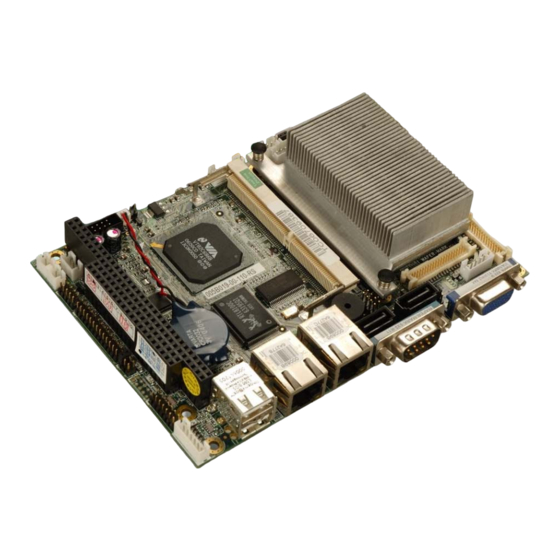
WAFER-MARK 3.5” Embedded SBC 1.2 WAFER-MARK Overview Figure 1-2: WAFER-MARK Overview Page 4... -
Page 25: Wafer-Mark Connectors
WAFER-MARK 3.5” Embedded SBC Figure 1-3: WAFER-MARK Solder Side Overview 1.2.1 WAFER-MARK Connectors The WAFER-MARK has the following connectors on-board: 1 x AT power connector 1 x ATX power supply enable connector 1 x Audio connector 1 x Audio CD in connector... -
Page 26: Technical Specifications
1 x TFT LCD LVDS connector 1 x TFT LCD TTL connector 1 x USB connector The WAFER-MARK has the following connectors on the board rear panel: 2 x Ethernet connectors 2 x USB connectors 1 x Keyboard/Mouse connector (optional) - Page 27 WAFER-MARK 3.5” Embedded SBC Specification WAFER-MARK Form Factor 3.5” form factor Embedded VIA Mark CoreFusion Low Voltage processor at 533MHz/800MHz Southbridge VIA VT82C686B VGA integrated in VIA Mark Display 24-bit TTL 18-bit dual channel LVDS Supports one 512MB DDR PC100/133MHz 144-pin SO-DIMM...
-
Page 28: Table 1-2: Technical Specifications
WAFER-MARK 3.5” Embedded SBC 5%~95% non-condensing Humidity (operating) Dimensions 146mm x 102mm Weight (GW/NW) 700g/260g Table 1-2: Technical Specifications Page 8... -
Page 29: Detailed Specifications
WAFER-MARK 3.5” Embedded SBC Chapter Detailed Specifications Page 9... -
Page 30: Overview
WAFER-MARK 3.5” Embedded SBC 2.1 Overview This chapter describes the specifications and on-board features of the WAFER-MARK in detail. 2.2 Dimensions 2.2.1 Board Dimensions The dimensions of the board are listed below: Length: 146mm Width: 102mm Figure 2-1: WAFER-MARK Dimensions (mm) 2.2.2 External Interface Panel Dimensions... -
Page 31: Data Flow
Figure 2-2: External Interface Panel Dimensions (mm) 2.3 Data Flow The WAFER-MARK motherboard comes with a VIA Mark CPU and a VIA VT82C686B Southbridge. Figure 2-3 shows the data flow between the system chipset, the CPU and other components installed on the motherboard. -
Page 32: Cpu Support
WAFER-MARK 3.5” Embedded SBC 2.4 CPU Support The WAFER-MARK series motherboards all come with a preinstalled 500MHz or 800MHz VIA Mark CPU. 2.4.1 VIA MARK Overview The specifications for the VIA Mark CPU are listed below 533MHz or 800MHz CPU frequency... -
Page 33: Via Mark S3 Graphics Prosavage4 Graphics Core
Please visit the VIA website for more information (http://www.via.com.tw/en/initiatives/padlock/index.jsp). 2.5 System Chipset The WAFER-MARK series motherboards all have a preinstalled VIA VT82C686B chipset. The system chipset features are listed below. Integrated AC'97 audio... -
Page 34: Via Vt82C686B Ata-6 Controller
Table 2-1: Supported HDD Specifications 2.5.2 VIA VT82C686B Flash Interface The WAFER-MARK CompactFlash socket supports standard CF Type I and CF Type II cards. The chipset flash interface is multiplexed with an IDE interface and can be connected to an array of industry standard NAND Flash or NOR Flash devices. -
Page 35: Via Vt82C686B Audio Codec 97 (Ac'97) Controller
WAFER-MARK 3.5” Embedded SBC 2.5.3 VIA VT82C686B Audio Codec 97 (AC’97) Controller The AC’97 specification v2.3 compliant controller on the chipset is interfaced to a 16-bit full-duplex AC'97 2.3 RealTek ALC655 codec. The ALC655 is then connected to a 10-pin audio connector to which an audio kit can easily be connected. -
Page 36: Via Vt82C686B Usb Controller
Configuration Panel for improved user convenience 2.5.4 VIA VT82C686B USB Controller Four internal USB ports on the WAFER-MARK board are interfaced via the PCI bus to the VIA VT82C686B chipset USB 1.1 controller. Four USB 1.1 devices can be connected simultaneously to the WAFER-MARK. -
Page 37: Via Vt82C686B Keyboard And Mouse
RAM. 2.5.10 BIOS The BIOS flash memory chip on the WAFER-MARK has a licensed copy of AWARD BIOS loaded onto it. The BIOS flash memory chip is connected to the VIA VT82C686B system chipset. The flash BIOS features are listed below:... -
Page 38: Pci Bus
Ethernet controller is interfaced through first the PCI bus a to the CPU and system chipset. The RealTek RTL8100C controller provides 10Mbps or 100Mbps Ethernet connectivity to the WAFER-MARK. Some of the features of the RealTek RTL8100C are listed below. 10Mbps and 100Mbps operation... -
Page 39: Sata Drive Controller
32bit wide, 66MHz PCI bus supported 2.7 Environmental and Power Specifications 2.7.1 System Monitoring The WAFER-MARK is capable of self-monitoring various aspects of its operating status including: Different component voltages including the CPU, chipset, and battery RPM of cooling fans CPU and system temperatures (by the corresponding embedded sensors) 2.7.2 Operating Temperature and Temperature Control... -
Page 40: Power Consumption
CPU surface to the heat sink. 2.7.3 Power Consumption Table 2-2 shows the power consumption parameters for a WAFER-MARK with a 533MHz CPU onboard and 800MHz CPU onboard. CPU Speed... -
Page 41: Unpacking
WAFER-MARK 3.5” Embedded SBC Chapter Unpacking Page 21... -
Page 42: Anti-Static Precautions
When the WAFER-MARK is unpacked, please do the following: Follow the anti-static precautions outlined in Section 3.1. Make sure the packing box is facing upwards so the WAFER-MARK does not fall out of the box. Make sure all the components shown in Section 3.3 are present. -
Page 43: Unpacking Checklist
If some of the components listed in the checklist below are missing, please do not proceed with the installation. Contact the IEI reseller or vendor you purchased the WAFER-MARK from or contact an IEI sales representative directly. To contact an IEI sales representative, please send an email to sales@iei.com.tw. -
Page 44: Optional Components
WAFER-MARK 3.5” Embedded SBC Dual ports serial port cable (P/N: 32200-026500-RS) Mini jumper Pack (P/N: 33100-000079-RS) Quick Installation Guide Utility CD Table 3-1: Package List Contents 3.3.2 Optional Components The following optional components are available from IEI. Item and Part Number... -
Page 45: Connector Pinouts
WAFER-MARK 3.5” Embedded SBC Chapter Connector Pinouts Page 25... -
Page 46: Peripheral Interface Connectors
WAFER-MARK 3.5” Embedded SBC 4.1 Peripheral Interface Connectors Section 4.1.2 shows peripheral interface connector locations. Section 4.1.2 lists all the peripheral interface connectors seen in Section 4.1.2. 4.1.1 WAFER-MARK Layout Figure 4-1 shows the on-board peripheral connectors, rear panel peripheral connectors and on-board jumpers. -
Page 47: Peripheral Interface Connectors
WAFER-MARK 3.5” Embedded SBC Figure 4-2: Connector and Jumper Locations (Solder Side) 4.1.2 Peripheral Interface Connectors Table 4-1 shows a list of the peripheral interface connectors on the WAFER-MARK. Detailed descriptions of these connectors can be found below. Connector Type... -
Page 48: External Interface Panel Connectors
40-pin crimp connector CN28 USB connector 8-pin header CN24 Table 4-1: Peripheral Interface Connectors 4.1.3 External Interface Panel Connectors Table 4-2 lists the rear panel connectors on the WAFER-MARK. Detailed descriptions of these connectors can be found in Section 4.3. Page 28... -
Page 49: Internal Peripheral Connectors
Internal peripheral connectors are found on the motherboard and are only accessible when the motherboard is outside of the chassis. This section has complete descriptions of all the internal, peripheral connectors on the WAFER-MARK. 4.2.1 AT Power Connector CN Label:... -
Page 50: Atx Power Supply Enable Connector
A jumper cap is installed on pin 1 and pin 2 as factory default (pin1=+5VSB; pin2=+5V). If the WAFER-MARK is connected to an AT power, let the jumper stay on pin 1 and pin 2. If connected to an ATX power source, remove the jumper cap. -
Page 51: Audio Connector
WAFER-MARK 3.5” Embedded SBC on/off switch to the power button connector (CN13). Please refer to Section 5.6.4 for more details. Note that the ATX power supply should provide a 10mA load on the 5V source standby lead for this function to take effect. -
Page 52: Audio Cd In Connector
WAFER-MARK 3.5” Embedded SBC Figure 4-5: Audio Connector Pinouts (10-pin) PIN NO. DESCRIPTION PIN NO. DESCRIPTION Line out R Line in R Line out L Line in L MIC in Table 4-5: Audio Connector Pinouts (10-pin) 4.2.4 Audio CD In Connector... -
Page 53: Backlight Inverter Connector
4.2.5 Backlight Inverter Connector CN Label: CN Type: 5-pin wafer (1x5) CN Location: See Figure 4-7 CN Pinouts: See Table 4-7 The backlight inverter connector provides the backlight on the LCD display connected to the WAFER-MARK with +12V of power. Page 33... -
Page 54: Battery Connector
WAFER-MARK 3.5” Embedded SBC Figure 4-7: Panel Backlight Connector Pinout Locations PIN NO. DESCRIPTION LCD_Adj [GND (Fixed mode): Maximum Brightness] GROUND +12V GROUND BACKLIGHT ENABLE Table 4-7: Panel Backlight Connector Pinouts 4.2.6 Battery Connector CN Label: CN Type: 2-pin wafer (1x2) -
Page 55: Compact Flash Socket
WAFER-MARK 3.5” Embedded SBC Figure 4-8: Battery Connector Location PIN NO. DESCRIPTION Battery+ Ground Table 4-8: Battery Connector Pinouts 4.2.7 Compact Flash Socket CN Label: CN32 (solder side) CN Type: 50-pin slot (2x25) CN Location: See Figure 4-9 CN Pinouts:... -
Page 56: Figure 4-9: Cf Card Socket Location
WAFER-MARK 3.5” Embedded SBC Figure 4-9: CF Card Socket Location Page 36... -
Page 57: Fan Connector
WAFER-MARK 3.5” Embedded SBC PIN NO. DESCRIPTION PIN NO. DESCRIPTION GROUND CFD2 SDD3 SDD11 SDD4 SDD12 SDD5 SDD13 SDD6 SDD14 SDD7 SDD15 SDCS1# SDCS3# GROUND GROUND SDIOR# GROUND SDIOW# GROUND GROUND IRQ15 GROUND MASTER/SLAVE GROUND GROUND RESET# GROUND SIORDY SDA2... -
Page 58: Floppy Disk Connector (Optional)
WAFER-MARK 3.5” Embedded SBC CN Location: See Figure 4-10 CN Pinouts: See Table 4-10 The cooling fan connector provides a 5V, 500mA current to a system cooling fan. The connector has a "rotation" pin to get rotation signals from fans and notify the system so the system BIOS can recognize the fan speed. -
Page 59: Figure 4-11: 26-Pin Fdd Connector Location
WAFER-MARK 3.5” Embedded SBC The floppy disk connector is connected to a floppy disk drive. Figure 4-11: 26-Pin FDD Connector Location PIN NO. DESCRIPTION PIN NO. DESCRIPTION INDEX- DISKSEL0- DSKCHG- MTR0- DIR- STEP- GROUND WDATA- GROUND WGATE- GROUND TRAK0- GROUND... -
Page 60: Gpio Connector
WAFER-MARK 3.5” Embedded SBC Table 4-11: 26-pin FDD Connector Pinouts 4.2.10 GPIO Connector CN Label: CN14 CN Type: 10-pin header (2x5) CN Location: See Figure 4-12 CN Pinouts: See Table 4-12 The GPIO connector can be connected to external I/O control devices including sensors, lights, alarms and switches. -
Page 61: Ide Connector
WAFER-MARK 3.5” Embedded SBC 4.2.11 IDE Connector CN Label: CN30 CN Type: 44-pin box header (2x22) CN Location: See Figure 4-13 CN Pinouts: See Table 4-13 One 44-pin IDE device connector on the WAFER-MARK supports connectivity to two hard disk drives. Page 41... -
Page 62: Figure 4-13: Secondary Ide Device Connector Locations
WAFER-MARK 3.5” Embedded SBC Figure 4-13: Secondary IDE Device Connector Locations PIN NO. DESCRIPTION PIN NO. DESCRIPTION RESET# GROUND DATA 7 DATA 8 DATA 6 DATA 9 DATA 5 DATA 10 DATA 4 DATA 11 DATA 3 DATA 12 DATA 2... -
Page 63: Infrared Interface Connector
WAFER-MARK 3.5” Embedded SBC HDC CS1# HDC CS3# HDD ACTIVE# GROUND GROUND Table 4-13: Secondary IDE Connector Pinouts 4.2.12 Infrared Interface Connector CN Label: CN27 CN Type: 5-pin wafer (1x5) CN Location: See Figure 4-14 CN Pinouts: See Table 4-14 The infrared interface connector supports both Serial Infrared (SIR) and Amplitude Shift Key Infrared (ASKIR) interfaces. -
Page 64: Keyboard/Mouse Connector
WAFER-MARK 3.5” Embedded SBC PIN NO. DESCRIPTION IR-RX IR-TX Table 4-14: Infrared Connector Pinouts 4.2.13 Keyboard/Mouse Connector CN Label: CN17 CN Type: 6-pin wafer (1x6) CN Location: See Figure 4-15 CN Pinouts: See Table 4-15 The keyboard and mouse connector can be connected to a standard PS/2 cable or PS/2 Y-cable to add keyboard and mouse functionality to the system. -
Page 65: Led Connector
WAFER-MARK 3.5” Embedded SBC KB CLK GROUND Table 4-15: Keyboard/Mouse Connector Pinouts 4.2.14 LED Connector CN Label: 6-pin wafer (1x6) CN Type: CN Location: See Figure 4-16 CN Pinouts: See Table 4-16 The LED connector connects to an HDD indicator LED and a power LED on the system chassis to inform the user about HDD activity and the power on/off status of the system. -
Page 66: Parallel Port Connector
WAFER-MARK 3.5” Embedded SBC IDE _ LED- Table 4-16: LED Connector Pinouts 4.2.15 Parallel Port Connector CN Label: CN15 CN Type: 26-pin header CN Location: See Figure 4-17 CN Pinouts: See Table 4-17 The 26-pin parallel port connector connects to a parallel port connector interface or some other parallel port device such as a printer. -
Page 67: Pc/104 Slot
WAFER-MARK 3.5” Embedded SBC DATA 5 GROUND DATA 6 GROUND DATA 7 GROUND ACKNOWLEDGE GROUND BUSY GROUND PAPER EMPTY GROUND PRINTER SELECT Table 4-17: Parallel Port Connector Pinouts 4.2.16 PC/104 Slot CN Label: CN10 CN Type: 104-pin PC/104 slot CN Location:... -
Page 68: Figure 4-18: Pc/104 Slot Location
WAFER-MARK 3.5” Embedded SBC Figure 4-18: PC/104 Slot Location Page 48... - Page 69 WAFER-MARK 3.5” Embedded SBC Pin No. Column A Column B Column C Column D IOCHK- GROUND GROUND GROUND RSTDRV SBHE- MCS16- SA23 IOCS16- IRQ9 SA22 IRQ10 SA21 IRQ11 DREQ2 SA20 IRQ12 -12V SA19 IRQ15 ZWS- SA18 IRQ14 +12V SA17 DACK0-...
-
Page 70: Pc/104 Power Input Connector
WAFER-MARK 3.5” Embedded SBC ISA_OSC GROUND GROUND GROUND Table 4-18: PC/104 Slot Connector Pinouts 4.2.17 PC/104 Power Input Connector CN Label: CN11 3-pin wafer (1x3) CN Type: CN Location: See Figure 4-19 CN Pinouts: See Table 4-19 The PC/104 power input connector provides power to the PC/104 expansion module installed on the PC/104 slot. -
Page 71: Power Button Connector
WAFER-MARK 3.5” Embedded SBC Table 4-19: PC/104 Power Input Connector Pinouts 4.2.18 Power Button Connector CN Label: CN13 CN Type: 2-pin wafer (1x2) CN Location: See Figure 4-20 CN Pinouts: See Table 4-20 The power button connector is connected to a power switch on the system chassis to enable users to turn the system on and off. -
Page 72: Sata Drive Connectors
WAFER-MARK 3.5” Embedded SBC CN Pinouts: See Table 4-21 The reset button connector is connected to a reset switch on the system chassis to enable users to reboot the system when the system is turned on. Figure 4-21: Reset Button Connector Locations PIN NO. -
Page 73: Serial Port Connector (Rs-422/485)
WAFER-MARK 3.5” Embedded SBC Figure 4-22: SATA Drive Connector Locations PIN NO. DESCRIPTION Table 4-22: SATA Drive Connector Pinouts 4.2.21 Serial Port Connector (RS-422/485) CN Label: CN16 CN Type: 14-pin header (2x20) CN Location: See Figure 4-23 CN Pinouts: See Table 4-23 The 14-pin serial port connector connects to the COM 2 serial communications channels. -
Page 74: Tft Lcd Lvds Connector
WAFER-MARK 3.5” Embedded SBC Figure 4-23: Serial Port Connector Pinout Locations PIN NO. DESCRIPTION PIN NO. DESCRIPTION Table 4-23: Serial Port Connector Pinouts 4.2.22 TFT LCD LVDS Connector CN Label: CN29 CN Type: 30-pin crimp (2x15) CN Location: See Figure 4-24... -
Page 75: Figure 4-24: Tft Lcd Lvds Connector Pinout Locations
WAFER-MARK 3.5” Embedded SBC Figure 4-24: TFT LCD LVDS Connector Pinout Locations PIN NO. DESCRIPTION PIN NO. DESCRIPTION GROUND GROUND LVDSA_Y0+ LVDSA_Y0- LVDSA_Y1+ LVDSA_Y1- LVDSA_Y2+ LVDSA_Y2- LVDSA_CLK+ LVDSA_CLK- GROUND GROUND LVDSB_Y0+ LVDSB_Y0- LVDSB_Y1+ LVDSB_Y1- Page 55... -
Page 76: Tft Lcd Ttl Connector
WAFER-MARK 3.5” Embedded SBC LVDSB_Y2+ LVDSB_Y2- LVDSB_CLK+ LVDSB_CLK- GROUND GROUND VCC_LVDS VCC_LVDS VCC_LVDS VCC_LVDS Table 4-24: TFT LCD LVDS Port Connector Pinouts 4.2.23 TFT LCD TTL Connector CN Label: CN28 CN Type: 40-pin crimp (2x20) CN Location: See Figure 4-25... -
Page 77: Figure 4-25: Tft Lcd Ttl Connector Pinout Locations
WAFER-MARK 3.5” Embedded SBC Figure 4-25: TFT LCD TTL Connector Pinout Locations PIN NO. DESCRIPTION PIN NO. DESCRIPTION VCC_FP VCC_FP GROUND GROUND VCC_FP VCC_FP GROUND Page 57... -
Page 78: Usb Connector (Internal)
WAFER-MARK 3.5” Embedded SBC GROUND GROUND FPCLK FPVS FPDE FPHS ENVEE Table 4-25: TFT LCD TTL Port Connector Pinouts 4.2.24 USB Connector (Internal) CN Label: CN24 8-pin header (2x4) CN Type: CN Location: See Figure 4-26 CN Pinouts: See Table 4-26 The 2x4 USB pin connectors each provide connectivity to two USB 1.1 ports. -
Page 79: External Peripheral Interface Connectors
Table 4-26: USB Port Connector Pinouts 4.3 External Peripheral Interface Connectors 4.3.1 External Peripheral Interface Connector Overview The WAFER-MARK external peripheral interface connectors are listed below and shown in Figure 4-27: 2 x RJ-45 Ethernet connectors 1 x Keyboard/Mouse connector... -
Page 80: Keyboard/Mouse Connector (Optional)
WAFER-MARK 3.5” Embedded SBC The RJ-45 Ethernet connector on the WAFER-MARK provides connectivity to a 10/100 megabits Ethernet connection between the WAFER-MARK and a Local Area Network (LAN) through a network hub. DESCRIPTION DESCRIPTION GROUND ACT_LED- ACT_LED+ LINK_LED - GROUNG... -
Page 81: Serial Port Connector (Com 1)
WAFER-MARK 3.5” Embedded SBC PS/2 CN Type: CN Pinouts: See Figure 4-29 and Table 4-29 The WAFER-MARK keyboard and mouse connector is a standard PS/2 connector. Figure 4-29: PS/2 Pinout and Configuration DESCRIPTION KB DATA MS DATA KB CLOCK MS CLOCK Table 4-29: Keyboard Connector Pinouts 4.3.4 Serial Port Connector (COM 1) -
Page 82: Usb Combo Port
WAFER-MARK 3.5” Embedded SBC PIN NO. DESCRIPTION PIN NO. DESCRIPTION DCD1 RXD1 TXD1 DTR1 DSR1 RTS1 CTS1 COM_RI1 Table 4-30: RS-232 Serial Port (COM 1) Pinouts Figure 4-30: COM1 Pinout Locations 4.3.5 USB Combo Port CN Label: CN19 CN Type:... -
Page 83: Vga Connector
WAFER-MARK 3.5” Embedded SBC DATA0- DATA1- DATA0+ DATA1+ GROUND GROUND Table 4-31: USB Connector Pinouts 4.3.6 VGA Connector CN Label: CN26 CN Type: DB15 CN Location: See Figure 4-27 CN Pinouts: See Figure 4-31 and Table 4-32 The standard 15-pin female DB15 VGA connector connects to a CRT or LCD monitor directly. - Page 84 WAFER-MARK 3.5” Embedded SBC THIS PAGE IS INTENTIONALLY LEFT BLANK Page 64...
-
Page 85: Installation
WAFER-MARK 3.5” Embedded SBC Chapter Installation Page 65... -
Page 86: Anti-Static Precautions
WAFER-MARK and severe injury to the user. Electrostatic discharge (ESD) can cause serious damage to electronic components, including the WAFER-MARK. Dry climates are especially susceptible to ESD. It is therefore critical that whenever the WAFER-MARK, or any other electrical component is handled, the following anti-static precautions are strictly adhered to. -
Page 87: Installation Considerations
The following installation notices and installation considerations should be read and understood before the WAFER-MARK is installed. All installation notices pertaining to the installation of the WAFER-MARK should be strictly adhered to. Failing to adhere to these precautions may lead to severe damage of the WAFER-MARK and injury to the person installing the motherboard. -
Page 88: Installation Checklist
5.2.2 Installation Checklist The following checklist is provided to ensure the WAFER-MARK is properly installed. All the items in the packing list are present (see Chapter 4) A compatible memory module is properly inserted into the slot (see Chapter... -
Page 89: So-Dimm Installation And Cf Card Installation
Figure 5-1. Figure 5-1: SO-DIMM Installation Step 1: Locate the SO-DIMM socket. Place the WAFER-MARK on an anti-static pad with the solder side facing up. Step 2: Align the SO-DIMM with the socket. The SO-DIMM must be oriented in such a way that the notch in the middle of the SO-DIMM must be aligned with the plastic bridge in the socket. -
Page 90: Cf Card Installation
The WAFER-MARK can support both CF Type I cards and CF Type II cards. For the complete specifications of the supported CF cards please refer to Chapter 2. To install the a CF card (Type 1 or Type 2) onto the WAFER-MARK, please follow the steps below: Step 1: Locate the CF card socket. -
Page 91: Jumper Settings
WAFER-MARK 3.5” Embedded SBC Figure 5-2: CF Card Installation 5.4 Jumper Settings NOTE: A jumper is a metal bridge that is used to close an electrical circuit. It consists of two metal pins and a small metal clip (often protected by a plastic cover) that slides over the pins to connect them. -
Page 92: Clear Cmos Jumper
Jumper Location: See Figure 5-3 If the WAFER-MARK fails to boot due to improper BIOS settings, the CMOS can be cleared using the battery connector. Disconnect the battery from the connector for a few seconds then reconnect the battery. The CMOS should be cleared. -
Page 93: Com 2 Function Select Jumper
WAFER-MARK 3.5” Embedded SBC The clear CMOS jumper settings are shown in Table 5-2. Clear CMOS Description Open Keep CMOS Setup Default Short Clear CMOS Setup Table 5-2: Clear CMOS Jumper Settings The location of the clear CMOS jumper is shown in Figure 5-3 below. -
Page 94: Lcd Voltage Selection
Figure 5-4: COM 2 Function Select Jumper Location 5.4.3 LCD Voltage Selection WARNING: Permanent damage to the screen and WAFER-MARK may occur if the wrong voltage is selected with this jumper. Please refer to the user guide that came with the monitor to select the correct voltage. -
Page 95: Com 1/2 Pin 9 Setting Jumper (Optional)
WAFER-MARK 3.5” Embedded SBC See Figure 5-5 Jumper Location: The LCD Voltage Selection jumper allows the LCD screen voltage to be set. The LCD Voltage Selection jumper settings are shown in Table 5-4. LCD Voltage Select Description Short 1-2 +3.3V LVDS... -
Page 96: Figure 5-6: Com 1/2 Pin 9 Setting Jumper Location
WAFER-MARK 3.5” Embedded SBC See Figure 5-6 Jumper Location: The COM 1/2 Pin 9 Setting jumper configures pin 9 on COM 1 (CN22) and COM 2 (CN16) as either a +5V, +12V power source or as a ring-in (RI) line. The COM 1/2 Pin 9 Setting jumper selection options are shown in Table 5-5. -
Page 97: Chassis Installation
The WAFER-MARK must be installed in a chassis with ventilation holes on the sides allowing airflow to travel through the heat sink surface. In a system with an individual power supply unit, the cooling fan of a power supply can also help generate airflow through the board surface. -
Page 98: Audio Kit Installation
The Audio Kit that came with the WAFER-MARK connects to the 10-pin audio connector on the WAFER-MARK. The audio kit consists of three audio jacks. One audio jack, Mic In, connects to a microphone. The remaining two audio jacks, Line-In and Line-Out, connect to two speakers. -
Page 99: Ata Flat Cable Connection
WAFER-MARK 3.5” Embedded SBC Step 0: 5.6.3 ATA Flat Cable Connection The IDE flat cable connects to the WAFER-MARK to one or two IDE devices. To connect an IDE HDD to the WAFER-MARK please follow the instructions below. Step 1: Locate the IDE connector. -
Page 100: Atx Power Connection
1 on the connectorStep 0: 5.6.4 ATX Power Connection Follow the instructions below to connect the WAFER-MARK to an ATX power supply. WARNING: Disconnect the power supply power cord from its AC power source to prevent a sudden power surge to the WAFER-MARK. -
Page 101: Figure 5-9: Power Cable To Motherboard Connection
WAFER-MARK 3.5” Embedded SBC Figure 5-9: Power Cable to Motherboard Connection Step 4: Connect ATX Power Adapter Cable to Power Supply. Connect the 20-pin ATX power adapter cable to an ATX power supply. See Figure 5-10. Figure 5-10: Connect ATX Power Adapter Cable to Power Supply Step 5: Connect ATX Power Cable to Motherboard. -
Page 102: Dual Rs-232 Cable Connection
WAFER-MARK 3.5” Embedded SBC 5-11. Figure 5-11: Connect ATX Power Cable to Motherboard Step 6: To turn on the system press the power button once. To turn off the power supply press the power button for about 4 seconds. Step 0: 5.6.5 Dual RS-232 Cable Connection... -
Page 103: Keyboard/Mouse Y-Cable Connector
The WAFER-MARK is shipped with a keyboard/mouse Y-cable connector. The keyboard/mouse Y-cable connector connects to a keyboard/mouse connector on the WAFER-MARK and branches into two cables that are each connected to a PS/2 connector, one for a mouse and one for a keyboard. To connect the keyboard/mouse Y-cable connector please follow the steps below. -
Page 104: Sata Drive Connection
Step 3: Insert the cable connectors. Once the cable connector is properly aligned with the keyboard/mouse connector on the WAFER-MARK, connect the cable connector to the onboard connectors. See Figure 5-13. Figure 5-13: Keyboard/mouse Y-cable Connection Step 4: Attach PS/2 connectors to the chassis. The keyboard/mouse Y-cable connector is connected to two PS/2 connectors. -
Page 105: Figure 5-14: Sata Drive Cable Connection
WAFER-MARK 3.5” Embedded SBC The WAFER-MARK is shipped with two SATA drive cables and one SATA drive power cable. To connect the SATA drives to the connectors, please follow the steps below. Step 1: Locate the connectors. The locations of the SATA drive connectors are shown in Chapter 3. -
Page 106: External Peripheral Interface Connection
USB devices VGA monitors RJ-45 Ethernet cable connectors To install these devices, connect the corresponding cable connector from the actual device to the corresponding WAFER-MARK external peripheral interface connector making sure the pins are properly aligned. 5.7.1 LAN Connection Page 86... -
Page 107: Serial Device Connection
RJ-45 connector into the onboard RJ-45 connector. Step 0: 5.7.2 Serial Device Connection The WAFER-MARK has a single female DB-9 connector on the external peripheral interface panel for a serial device. Follow the steps below to connect a serial device to the WAFER-MARK. -
Page 108: Usb Connection
WAFER-MARK 3.5” Embedded SBC Chapter 3. Step 2: Insert the serial connector. Insert the DB-9 connector of a serial device into the DB-9 connector on the external peripheral interface. See Figure 5-17. Figure 5-17: Serial Device Connector Step 3: Secure the connector. Secure the serial device connector to the external interface by tightening the two retention screws on either side of the connector. -
Page 109: Figure 5-18: Usb Connector
WAFER-MARK 3.5” Embedded SBC the USB Series "A" receptacle on the external peripheral interface. See Figure 5-18. Step 0: Figure 5-18: USB Connector Page 89... - Page 110 WAFER-MARK 3.5” Embedded SBC THIS PAGE IS INTENTIONALLY LEFT BLANK Page 90...
-
Page 111: Award Bios
WAFER-MARK 3.5” Embedded SBC Chapter AWARD BIOS Page 91... -
Page 112: Introduction
WAFER-MARK 3.5” Embedded SBC 6.1 Introduction A licensed copy of Phoenix Award BIOS is preprogrammed into the ROM BIOS. The BIOS setup program allows users to modify the basic system configuration. This chapter describes how to access the BIOS setup program and the configuration options that may be changed. -
Page 113: Getting Help
WAFER-MARK 3.5” Embedded SBC Item help Previous values for the page menu items Fail-safe defaults for the current page menu items Optimized defaults for the current page menu items Menu in BIOS Save changes and Exit BIOS Table 6-1: BIOS Navigation Keys 6.1.3 Getting Help... -
Page 114: Bios Menu 1: Award Bios Cmos Setup Utility
WAFER-MARK 3.5” Embedded SBC BIOS Menu 1: Award BIOS CMOS Setup Utility NOTE: The following sections will completely describe the menus listed below and the configuration options available to users. The following menu options are seen in BIOS Menu 1. - Page 115 WAFER-MARK 3.5” Embedded SBC The following user configurable options are also available in BIOS Menu 1: Load Fail-Safe Defaults Use the Load Fail-Safe Defaults option to load failsafe default values for each BIOS parameter in the setup menus. Press F6 for this operation on any page.
-
Page 116: Standard Cmos Features
WAFER-MARK 3.5” Embedded SBC Exit Without Saving Use the Exit Without Saving option to exit the BIOS menus without saving any configuration changes. 6.2 Standard CMOS Features Use the Standard CMOS Features BIOS menu (BIOS Menu 2) to set basic BIOS configuration options. -
Page 117: Ide Primary Master/Slave
WAFER-MARK 3.5” Embedded SBC IDE Master and IDE Slave When entering setup, BIOS auto detects the presence of IDE devices. The Standard CMOS Features menu shows the status of the auto detected IDE devices. The following IDE devices are detected and shown in the Standard CMOS Features menu:... - Page 118 WAFER-MARK 3.5” Embedded SBC IDE HDD Auto-Detection [Press Enter] Use the IDE HDD Auto-Detection option to enable BIOS to automatically detect the IDE settings. Select IDE HDD Auto-Detection and press E . BIOS automatically detects NTER the HDD type. Do not set this option manually.
- Page 119 WAFER-MARK 3.5” Embedded SBC Select this mode if the HDD capacity is less than 504MB. Select this mode if the HDD capacity is more than 8.4GB. Large This mode is an extended ECHS mode and while it supports HDDs larger...
-
Page 120: Advanced Bios Features
WAFER-MARK 3.5” Embedded SBC Sector The Sector specification indicates how many logical sectors the HDD has been divided into. 6.3 Advanced BIOS Features Use the Advanced BIOS Features menu (BIOS Menu 3) to configure the CPU and peripheral device configuration options. - Page 121 WAFER-MARK 3.5” Embedded SBC Boot From LAN Control [Disabled] Use the BOOT From LAN Control option to enable the system to be booted from a remote system. Disabled The system cannot be booted from a remote system EFAULT through the LAN.
-
Page 122: Advanced Chipset Features
WAFER-MARK 3.5” Embedded SBC CDROM HDD-1 HDD-2 HDD-3 ZIP100 USB-FDD USB-ZIP USB-CDROM USB-HDD Disabled Boot Other Device [Enabled] Use the Boot Other Device option to determine whether the system uses a second or third boot device if the first boot device is not found. -
Page 123: Bios Menu 4: Advanced Chipset Features
WAFER-MARK 3.5” Embedded SBC BIOS Menu 4: Advanced Chipset Features Memory Hole [Disabled] Use the Memory Hole option to reserve memory space between 15MB and 16MB for ISA expansion cards that require a specified area of memory to work properly. If an older ISA expansion card is used, please refer to the documentation that came with the card to see if it is necessary to reserve the space. -
Page 124: Integrated Peripherals
WAFER-MARK 3.5” Embedded SBC 1024 x 768 2ch LVDS 1024 x 768 36Bits 800 x 600 DSTN 1024 x 768 1ch LVDS 800 x 600 18Bits 1024 x 768 24Bits EFAULT Power Supply Type [ATX] Use the Power Supply Type option to specify whether an AT or ATX power supply is connected to the system. -
Page 125: Bios Menu 5: Integrated Peripherals
WAFER-MARK 3.5” Embedded SBC BIOS Menu 5: Integrated Peripherals On-Chip IDE Channel 0/1 [Enabled] Use the On-Chip IDE Channel 0/1 option to specify if the system uses the integrated primary IDE channel or not. Disabled The primary IDE channel is not used. - Page 126 WAFER-MARK 3.5” Embedded SBC Onboard Serial Port 1 [3F8/IRQ4] Use the Onboard Serial Port 1 option to select the I/O address and IRQ for the onboard serial port 1. The serial port can be disabled or the I/O address and the IRQ can be automatically selected by the BIOS.
- Page 127 WAFER-MARK 3.5” Embedded SBC x IR Function Duplex [Half] The IR Function Duplex option can only be configured if the UART 2 Mode is set to HPSIR or ASKIR. Use the IR Function Duplex option to enable bi-directional communication between the system infrared port and the external device.
- Page 128 WAFER-MARK 3.5” Embedded SBC Parallel Port Mode [Normal] Use the Parallel Port Mode option to select parallel port operation mode. Normal EFAULT The parallel port operates in the enhanced parallel port mode (EPP). The EPP mode supports bi-directional communication between the system and the parallel port device and the transmission rates between the two are much faster than the SPP mode.
-
Page 129: Power Management Setup
WAFER-MARK 3.5” Embedded SBC EPP1.9 EPP 1.9 is selected as the EPP standard. EFAULT EPP1.7 EPP 1.7 is selected as the EPP standard. 6.6 Power Management Setup Use the Power Management Setup menu (BIOS Menu 6) to set the BIOS power management and saving features. -
Page 130: Wake Up Events
WAFER-MARK 3.5” Embedded SBC ACPI Suspend Type [S1(POS)] Use the ACPI Suspend Type BIOS option to specify the sleep state the system enters when not being used. S1 (POS) System appears off. The CPU is stopped; RAM is EFAULT refreshed; the system is running in a low power mode. -
Page 131: Bios Menu 7: Wake Up Events
WAFER-MARK 3.5” Embedded SBC BIOS Menu 7: Wake Up Events Wake Up On LAN [Disabled] Use the Wake Up On LAN option to enable activity on the LAN to rouse the system from a suspend or doze state. Disabled Wake event not generated by LAN activity... -
Page 132: Pnp/Pci Configurations
WAFER-MARK 3.5” Embedded SBC RTC Alarm Resume [Disabled] Use the RTC Alarm Resume option to specify when the computer is roused from a suspended state. Disabled The real time clock (RTC) cannot generate a wake EFAULT event Enabled If selected, the following appears with values that... -
Page 133: Bios Menu 8: Pnp/Pci Configurations
WAFER-MARK 3.5” Embedded SBC BIOS Menu 8: PnP/PCI Configurations Resources Controlled By [Auto (ESCD)] Use the Resources Controlled By option to either manually configure all the boot and plug and play devices, or allow BIOS to configure these devices automatically. If BIOS is allowed to configure the devices automatically IRQs, DMA and memory base address fields cannot be set manually. - Page 134 WAFER-MARK 3.5” Embedded SBC IRQ-9 assigned to IRQ-10 assigned to IRQ-11 assigned to IRQ-12 assigned to IRQ-13 assigned to IRQ-14 assigned to IRQ-15 assigned to The above options all have the following default options. PCI/ISA PnP The IRQ is assigned to PCI/ISA PNP for devices compliant...
-
Page 135: Pc Health Status
WAFER-MARK 3.5” Embedded SBC Legacy ISA The IRQ is assigned to legacy ISA for devices compliant with the original PC AT bus specification. 6.8 PC Health Status The PC Health Status menu (BIOS Menu 9) has no user configurable options, but shows system operating parameters that are essential to the stable operation of the system. - Page 136 WAFER-MARK 3.5” Embedded SBC Voltages The following voltages are monitored: CPU Vcore VccMem +2.5 V +3.3 V +5 V +12 V Fan Speeds The following fan speeds are monitored: CPU Fan Speed Page 116...
-
Page 137: Software Drivers
WAFER-MARK 3.5” Embedded SBC Chapter Software Drivers Page 117... -
Page 138: Available Software Drivers
7.2 VIA 4 in 1 Chipset Driver Installation (VIA Service Pack v4.3) To install the chipset driver, please follow the steps below: Step 1: Insert the CD into the system that contains the WAFER-MARK board. Step 2: Open the “WAFER-MARK” folder. Open the “4in1 Extreme” subfolder. (See... -
Page 139: Figure 7-1: Access The 4In1_Extreme Folder
WAFER-MARK 3.5” Embedded SBC Figure 7-1: Access the 4in1_Extreme Folder Step 3: Click the Setup utility icon shown in Figure 7-2. Figure 7-2: Setup Utility Icon Step 4: The installation program begins to initialize. After the initialization process a welcome screen shown in Figure 7-3 appears. Click “N ”... -
Page 140: Figure 7-4: Readme Information
WAFER-MARK 3.5” Embedded SBC Step 5: The “Readme” in Figure 7-4 appears. Click “N ” to continue. Figure 7-4: Readme Information Step 6: Select “Normal Installation” or “Quick Installation.” (See Figure 7-5) Click “N ” to continue. Page 120... -
Page 141: Figure 7-5: Via Chipset Driver Installation Type
WAFER-MARK 3.5” Embedded SBC Figure 7-5: VIA Chipset Driver Installation Type Step 7: Select the setup components (see Figure 7-6) that must be installed in the system. There are setup components: VIA PCI IDE Bus Driver AGP Driver (AGP3.0 Supported) VIA INF Driver 1.70A... -
Page 142: Figure 7-6: Driver Selection
WAFER-MARK 3.5” Embedded SBC Figure 7-6: Driver Selection Step 8: The setup then prompts the user (see Figure 7-7) if the VIA PCI IDE Bus Driver must be installed on the system. Select install or uninstall. Click “N ” to continue. -
Page 143: Figure 7-7: Via Pci Ide Bus Driver Selection
WAFER-MARK 3.5” Embedded SBC Figure 7-7: VIA PCI IDE Bus Driver Selection Step 9: The setup then prompts the user (see Figure 7-8) if the AGP driver must be installed on the system. Select install or uninstall. Click “N ” to continue. -
Page 144: Figure 7-8: Agp Driver Selection
WAFER-MARK 3.5” Embedded SBC Figure 7-8: AGP Driver Selection Step 10: The drivers are then installed onto the system. After the installation is complete the user is prompted to restart the computer now or later. (See Figure 7-9) Select when the computer must be restarted. Click “OK” to exit the installation program.Step 0:... -
Page 145: Realtek Audio Driver Installation
7.3 RealTek Audio Driver Installation To install the RealTek AC’97 Audio driver, please follow the steps below: Step 1: Insert the CD into the system that contains the WAFER-MARK board. Step 2: Open the “WAFER-MARK” folder. Open the “Audio” subfolder. (See Figure... -
Page 146: Figure 7-11: Setup Utility Icon
WAFER-MARK 3.5” Embedded SBC Figure 7-11: Setup Utility Icon Step 4: The install shield wizard for the audio driver starts. See Figure 7-12. Figure 7-12: Audio Driver Install Shield Wizard Starting Step 5: The RealTek Audio Setup prepares the install shield to guide you through the rest of the setup process. -
Page 147: Figure 7-13: Audio Driver Setup Preparation
WAFER-MARK 3.5” Embedded SBC Figure 7-13: Audio Driver Setup Preparation Step 6: The welcome screen shown in Figure 7-14 appears. Click the “N ” button to continue the installation. The install shield starts to configure the new software as shown in Figure 7-15. -
Page 148: Figure 7-14: Audio Driver Welcome Screen
WAFER-MARK 3.5” Embedded SBC Figure 7-14: Audio Driver Welcome Screen Figure 7-15: Audio Driver Software Configuration Page 128... -
Page 149: Figure 7-16: Audio Driver Digital Signal
WAFER-MARK 3.5” Embedded SBC Step 7: The “Digital Signal Not Found” screen shown in Figure 7-16 appears. Click “Y ” to continue the installation. Figure 7-16: Audio Driver Digital Signal Step 8: The installation of the driver begins. See Figure 7-17. -
Page 150: Figure 7-17: Audio Driver Installation Begins
WAFER-MARK 3.5” Embedded SBC Figure 7-17: Audio Driver Installation Begins Step 9: After the driver installation process is complete, a confirmation screen shown in Figure 7-18 appears. Page 130... -
Page 151: Lan Driver Installation
7.3.1 LAN Driver Installation To install the LAN driver, follow the steps below: Step 1: Insert the CD into the system that contains the WAFER-MARK board. Step 2: Open the “WAFER-MARK” folder. Open the “LAN” subfolder. (See Figure 7-19) Figure 7-19: Access the LAN Driver Folder... -
Page 152: Figure 7-20: Setup Utility Icon
WAFER-MARK 3.5” Embedded SBC Step 3: Click the Setup utility icon shown in Figure 7-20. Figure 7-20: Setup Utility Icon Step 4: Once the Setup icon is double clicked, a Welcome screen shown in Figure 7-21 appears. Figure 7-21: LAN Driver Welcome Screen Step 5: To continue installing click “Next.”... -
Page 153: Figure 7-22: Lan Driver Installation Complete
WAFER-MARK 3.5” Embedded SBC Figure 7-22: LAN Driver Installation Complete Step 6: Click “Finish” to complete the installation. Step 0: Page 133... - Page 154 WAFER-MARK 3.5” Embedded SBC THIS PAGE IS INTENTIONALLY LEFT BLANK Page 134...
-
Page 155: Abios Options
WAFER-MARK 3.5” Embedded SBC Appendix BIOS Options Page 135... - Page 156 WAFER-MARK 3.5” Embedded SBC Load Fail-Safe Defaults .................95 Load Optimized Defaults ................95 Set Supervisor Password................95 Set User Password..................95 Save & Exit Setup...................95 Exit Without Saving..................96 Date [Day mm:dd:yyyy] .................96 Time [hh/mm/ss].....................96 ...
- Page 157 WAFER-MARK 3.5” Embedded SBC OnChip Sound [Auto] ................. 104 On-Chip IDE Channel 0/1 [Enabled] ............105 Init Display First [PCI Slot] ................. 105 Onboard Serial Port 1 [3F8/IRQ4] .............. 106 Onboard Serial Port 2 [2F8/IRQ3] .............. 106 ...
- Page 158 WAFER-MARK 3.5” Embedded SBC THIS PAGE IS INTENTIONALLY LEFT BLANK Page 138...
-
Page 159: Bgpio Connection
WAFER-MARK 3.5” Embedded SBC Appendix GPIO Connection Page 139... -
Page 160: Dio Interface Introduction
WAFER-MARK 3.5” Embedded SBC B.1 DIO Interface Introduction The DIO connector on the WAFER-MARK is interfaced to GIO ports on the VIA VT82C686B Super I/O chipset. The DIO has both 4-bit digital inputs and 4-bit digital outputs. The digital inputs and digital outputs are generally control signals that control the on/off circuit of external devices or TTL devices. -
Page 161: Assembly Language Samples
WAFER-MARK 3.5” Embedded SBC B.3 Assembly Language Samples B.3.1 Enable the DIO Input Function The BIOS interrupt call INT 15H controls the digital I/O. An assembly program to enable digital I/O input functions is listed below. AX, 6F08H Sets the digital port as input Initiates the INT 15H BIOS call B.3.2 Enable the DIO Output Function... - Page 162 WAFER-MARK 3.5” Embedded SBC THIS PAGE IS INTENTIONALLY LEFT BLANK Page 142...
-
Page 163: Cwatchdog Timer
WAFER-MARK 3.5” Embedded SBC Appendix Watchdog Timer Page 143... - Page 164 WAFER-MARK 3.5” Embedded SBC NOTE: The following discussion applies to DOS environment. IEI support is contacted or the IEI website visited for specific drivers for more sophisticated operating systems, e.g., Windows and Linux. The Watchdog Timer is provided to ensure that standalone systems can always recover from catastrophic conditions that cause the CPU to crash.
- Page 165 WAFER-MARK 3.5” Embedded SBC NOTE: When exiting a program it is necessary to disable the Watchdog Timer, otherwise the system resets. Example program: ; INITIAL TIMER PERIOD COUNTER W_LOOP: AX, 6F02H ;setting the time-out value BL, 30 ;time-out value is 48 seconds ;...
- Page 166 WAFER-MARK 3.5” Embedded SBC THIS PAGE IS INTENTIONALLY LEFT BLANK Page 146...
-
Page 167: Daddress Mapping
WAFER-MARK 3.5” Embedded SBC Appendix Address Mapping Page 147... -
Page 168: Address Map
WAFER-MARK 3.5” Embedded SBC D.1 Address Map I/O address Range Description 000-01F DMA Controller 020-021 Interrupt Controller 040-043 System time 060-06F Keyboard Controller 070-07F System CMOS/Real time Clock 080-09F DMA Controller 0A0-0A1 Interrupt Controller 0C0-0DF DMA Controller 0F0-0FF Numeric data processor... -
Page 169: Irq Mapping Table
WAFER-MARK 3.5” Embedded SBC D.3 IRQ Mapping Table IRQ0 System Timer IRQ8 RTC clock IRQ1 Keyboard IRQ9 ACPI IRQ2 Available IRQ10 IRQ3 COM2 IRQ11 LAN/USB2.0/SATA IRQ4 COM1 IRQ12 PS/2 mouse IRQ5 SMBus Controller IRQ13 IRQ6 IRQ14 Primary IDE IRQ7 Parallel Port... - Page 170 WAFER-MARK 3.5” Embedded SBC THIS PAGE IS INTENTIONALLY LEFT BLANK Page 150...
-
Page 171: Eexternal Ac'97 Audio Codec
WAFER-MARK 3.5” Embedded SBC Appendix External AC’97 Audio CODEC Page 151... -
Page 172: Introduction
16-bit, full duplex AC’97 Rev. 2.3 compatible audio CODECwith a sampling rate of 48KHz. E.1.1 Accessing the AC’97 CODEC The CODEC is accessed through a connector on the WAFER-MARK motherboard. Connect the audio kit to the connector. E.1.2 Driver Installation The driver installation has been described in Chapter 7. -
Page 173: Sound Effect Configuration
WAFER-MARK 3.5” Embedded SBC E.2 Sound Effect Configuration E.2.1 Accessing the Sound Effects Manager To access the Sound Effects Manager, please do the following: Step 1: Install the audio CODEC driver. Step 2: Click either: The Sound Effect Manager icon in the Notification Area of the system task bar (see Figure E-2), or The Sound Effect Manager icon in the Control Panel (Figure E-3). -
Page 174: Sound Effect Manager Configuration Options
WAFER-MARK 3.5” Embedded SBC NOTE: The Sound Effect Manager shown above is for the RealTek ALC655 audio CODEC. Different CODECs may have different sound manager appearances. The following section describes the different configuration options in the Sound Effect Manager. E.2.2 Sound Effect Manager Configuration Options The Sound Effects Manager enables configuration of the items listed below. - Page 175 WAFER-MARK 3.5” Embedded SBC Microphone Effect General NOTE: Not all RealTek Sound Effect Managers have all the above listed options. The Sound Effect Manager loaded onto the system may only have some of the options listed above. Below is a brief description of the available configuration options in the Sound Effects Manager.
- Page 176 WAFER-MARK 3.5” Embedded SBC S/PDIF-In & S/PDIF-Out:- These functions are currently not supported. Connector Sensing:- Realtek ALC655 detects if an audio device is plugged into the wrong connector. If an incorrect device is plugged in a warning message appears. HRTF Demo:- Adjust HRTF (Head Related Transfer Functions) 3D positional audio here before running 3D applications.
-
Page 177: Fraid Setup
WAFER-MARK 3.5” Embedded SBC Appendix RAID Setup Page 157... -
Page 178: Introduction
WAFER-MARK 3.5” Embedded SBC F.1 Introduction The ALi M5283 SATA RAID chipset can control parallel ATA (PATA) and serial ATA (SATA) disks. The ALi controller supports PATA UDMA transfer mode up to mode 6 and SATA 1 disk drives. The ALi M5283 also has a cost-effective RAID functionality that can increase the data read/write speed and provide protection to data by distributing mirrored duplicates of data onto two disk drives (RAID 1). -
Page 179: Features And Benefits
WAFER-MARK 3.5” Embedded SBC CAUTION: Do not accidentally disconnect the SATA drive cables. Carefully route the cables within the chassis to avoid system down time. F.2 Features and Benefits Supports RAID levels 0, 1, and JBOD Supports connectivity to two disk drives... - Page 180 WAFER-MARK 3.5” Embedded SBC 6.3) Step 6: Save and Exit BIOS. After the SATA BOOT ROM Control BIOS option is enabled, save and exit the BIOS. Step 7: Reboot the system. Reboot the system after saving and exiting the BIOS.
-
Page 181: Raid Options
WAFER-MARK 3.5” Embedded SBC Figure F-2: RAID BIOS Setup Utility Step 10: Configure the RAID settings. Use the RAID BIOS Setup Utility in Figure F-2 to configure the RAID array. Brief descriptions are given below. Step 11: Install the OS. After the RAID array has been configured (see below) install the OS. - Page 182 WAFER-MARK 3.5” Embedded SBC drives. Step 1: Select “Create RAID 0 Striping for Performance”. Use the arrow keys to highlight Create RAID0 Striping for Performance and press E . A flashing NTER ‘S’ appears on the Drive Menu where the member drives to be included in the RAID 0 array can be chosen.
-
Page 183: Create Raid 1 Mirroring For Reliability
WAFER-MARK 3.5” Embedded SBC F.4.2 Create RAID 1 Mirroring for Reliability WARNING: All data previously stored on the member drives of a RAID configuration is destroyed during the RAID initialization process. If “used” drives are used to create a RAID array, make sure the data has been moved or backed up before creating a RAID array out of the disk drives. - Page 184 WAFER-MARK 3.5” Embedded SBC Step 3: Confirm. The Create RAID0(Y/N) confirm box appears. Press Y. Step 4: Name the array. Enter a nickname for the created array. Upper and lower case alphabetic, numeric, space, and underscore characters are all applicable for...
-
Page 185: Create Jbod For Integrated Capacity
WAFER-MARK 3.5” Embedded SBC F.4.3 Create JBOD for Integrated Capacity JBOD is defined as “Just a Bunch of Drives.” JBOD provides neither performance gains nor data redundancy. WARNING: All data previously stored on the member drives of a RAID configuration is destroyed during the RAID initialization process. If “used”... -
Page 186: Stripe Size
WAFER-MARK 3.5” Embedded SBC can be chosen. Step 2: Select RAID array drive members. Use the space bar to select members of the RAID array. The flashing cursor changes to a lower case ‘s’ once any of the connected disk drives has been selected. Follow the same method to select another member drive. -
Page 187: Delete Raid Setting & Partition
WAFER-MARK 3.5” Embedded SBC A/V playback and editing applications. The default value should be appropriate for most applications. F.4.5 Delete RAID Setting & Partition WARNING: If a RAID configuration is deleted, all data previously stored on the member drives of the RAID configuration will also be deleted. -
Page 188: Rebuild Raid Array
WAFER-MARK 3.5” Embedded SBC F.4.7 Rebuild RAID Array The Rebuild RAID Array option can rebuild a RAID array if a member of a RAID configuration should fail. Neither RAID 0 nor JBOD provides data redundancy. The Rebuild RAID Array option only applies to RAID1 arrays and is applicable when a member of a RAID1 configuration has failed. -
Page 189: Gindex
WAFER-MARK 3.5” Embedded SBC Index Page 169... - Page 190 WAFER-MARK 3.5” Embedded SBC audio connector CD in------------------------- 32 1 location and pinouts ------------------------ 32 audio kit ------------------------------------------- 78 10/100 megabits---------------------------- 18, 60 installation ------------------------------------ 78 10/100M Ethernet -------------------------------18 Award BIOS------------------------------------- 159 3 B 3.5" form factor --------------------------------- 3 backlight inverter connector------------------ 33 location and pinouts ------------------------ 33 A...
- Page 191 WAFER-MARK 3.5” Embedded SBC floppy disk ------------------------------------ 38 clear CMOS connector ---------------------34 clear CMOS jumper -------------------------72 GPIO ------------------------------------------- 40 codec-----------------------------------------------15 IDE---------------------------------------------- 41 AC’97 -------------------------------------------15 infrared interface ---------------------------- 43 COM 1 keyboard/mouse ---------------------------- 44 pin 9 setup jumper---------------------------75 LED--------------------------------------------- 45 COM 1 pin 9 setting jumper-------------------75...
- Page 192 WAFER-MARK 3.5” Embedded SBC RJ-45 cable connector ---------------------86 I RJ-45 connector -----------------------------60 IDE connector, 44-pin ------------------------- 41 Ethernet connector------------------------------59 location and pinouts ------------------------ 41 Ethernet connectors ----------------------------- 6 IDE controller ------------------------------------ 14 Ethernet controller ------------------------------18 IDE device------------------------------------78, 79 external peripheral interface ------------------86...
- Page 193 WAFER-MARK 3.5” Embedded SBC location and pinouts-------------------------44 P keyboard/mouse connector -------------------17 parallel port connector------------------------- 46 L location and pinouts ------------------------ 46 parallel port connector------------------------- 17 LAN connection----------------------------------86 PC/104 power input connector -------------- 50 LCD display---------------------------------- 33, 74 location and pinouts ------------------------ 50...
- Page 194 WAFER-MARK 3.5” Embedded SBC specifcations --------------------------------- 69 connector location and pinouts ------ 53, 61 dual cable--------------------------------------82 SO-DIMM socket --------------------------------- 6 RS-232 serial port connector -----------------16 software drivers -------------------------------- 118 RS-422---------------------------------------- 53, 73 Super I/O ----------------------------------------- 13 COM 2 location and pinouts---------------53...
- Page 195 WAFER-MARK 3.5” Embedded SBC USB connectors ---------------------------------- 6 VIA processor-------------------------------------- 2 USB device connection ------------------------88 video capture port ------------------------------ 13 dual connector--------------------------------88 W V warranty validation ----------------------------- 68 VGA ------------------------------------------------63 Y connector --------------------------------------59 connector pinouts----------------------------63 Y-cable -------------------------------------------- 44 DB15 connector ------------------------------63...
Need help?
Do you have a question about the WAFER-MARK and is the answer not in the manual?
Questions and answers