
Related Manuals for Altera Cyclone IV GX


Summary of Contents for Altera Cyclone IV GX
- Page 1 Cyclone IV GX Transceiver Starter Board Reference Manual 101 Innovation Drive Document Version: San Jose, CA 95134 Document Date: March 2010 www.altera.com Downloaded from Elcodis.com electronic components distributor...
- Page 2 Altera warrants performance of its semiconductor products to current specifications in accordance with Altera's standard warranty, but reserves the right to make changes to any products and services at any time without notice. Altera assumes no responsibility or liability arising out of the application or use of any information, product, or service described herein except as expressly agreed to in writing by Altera Corporation.
-
Page 3: Table Of Contents
Cyclone IV GX Transceiver Clock Inputs ........ - Page 4 Cyclone IV GX Transceiver Starter Board Reference Manual © March 2010 Altera Corporation Downloaded from Elcodis.com electronic components distributor...
-
Page 5: Chapter 1. Overview
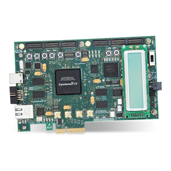
FPGA designs that interface with all components of the board. General Description The Cyclone IV GX transceiver starter board provides a hardware platform for developing and prototyping low-power, high-volume, feature-rich designs as well as to demonstrate the Cyclone IV GX device's on-chip memory, embedded multipliers, and the Nios ®... -
Page 6: Board Component Blocks
1–2 Chapter 1: Overview Board Component Blocks Board Component Blocks The board features the following major component blocks: ■ Cyclone IV GX EP4CGX15BF14 FPGA in the 169-pin FineLine BGA (FBGA) package 14,400 LEs ■ 540-kilobit (Kb) on-die memory ■ 20 global clocks ■... - Page 7 On/Off slide power switch ■ On-Board power measurement circuitry ■ Mechanical ■ 6.6” x 2.713” board ■ PCI Express chassis or bench-top operation ■ © March 2010 Altera Corporation Cyclone IV GX Transceiver Starter Board Reference Manual Downloaded from Elcodis.com electronic components distributor...
-
Page 8: Starter Board Block Diagram
1–4 Chapter 1: Overview Starter Board Block Diagram Starter Board Block Diagram Figure 1–1 shows the block diagram of the Cyclone IV GX transceiver starter board. Figure 1–1. Cyclone IV GX transceiver Starter Board Block Diagram Push-button User LEDs Switches... -
Page 9: Introduction
A complete set of schematics, a physical layout database, and GERBER files for the starter board reside in the Cyclone IV GX Transceiver starter kit documents directory. For information about powering up the board and installing the demonstration... - Page 10 (C58, C59) Connector Connectors (U14) (J10, J11) Table 2–1 describes the components and lists their corresponding board references. Table 2–1. Cyclone IV GX Transceiver Starter Board Components (Part 1 of 3) Board Reference Type Description Featured Devices FPGA EP4CGX15BF14, 169-pin FBGA.
- Page 11 Chapter 2: Board Components 2–3 Board Overview Table 2–1. Cyclone IV GX Transceiver Starter Board Components (Part 2 of 3) Board Reference Type Description Load LED Illuminates when the MAX II CPLD EPM2210 System Controller is actively configuring the FPGA.
-
Page 12: Featured Device: Cyclone Iv Gx Device
2–4 Chapter 2: Board Components Featured Device: Cyclone IV GX Device Table 2–1. Cyclone IV GX Transceiver Starter Board Components (Part 3 of 3) Board Reference Type Description J8, J9 Transceiver RX SMA connectors Two input SMAs (optional) to the high-speed positive and negative differential receiver channel. -
Page 13: I/O Resources
Bank 5A Bank Name Number of I/Os Table 2–4 lists the Cyclone IV GX device pin count and usage by function on the starter board. Table 2–4. Cyclone IV GX Device I/O Pin Count and Usage (Note 1) Function I/O Standard... -
Page 14: Max Ii Cpld Epm2210 System Controller
2–6 Chapter 2: Board Components MAX II CPLD EPM2210 System Controller MAX II CPLD EPM2210 System Controller The board utilizes the EPM2210 System Controller, an Altera MAX II CPLD, for the following purposes: ■ FPGA configuration from flash memory ■... - Page 15 FSML_A21 FSML bus address FSML_A22 FSML bus address FSML_A23 FSML bus data FSML_D0 FSML bus data FSML_D1 FSML bus data FSML_D2 © March 2010 Altera Corporation Cyclone IV GX Transceiver Starter Board Reference Manual Downloaded from Elcodis.com electronic components distributor...
- Page 16 SRAM_ADVn FSML bus SSRAM clock SRAM_CLK Table 2–6 lists the MAX II CPLD EPM2210 System Controller component reference and manufacturing information. Cyclone IV GX Transceiver Starter Board Reference Manual © March 2010 Altera Corporation Downloaded from Elcodis.com electronic components distributor...
-
Page 17: Configuration, Status, And Setup Elements
The USB-Blaster is implemented using a USB Type-B connector (J5), a FTDI USB 2.0 PHY device (U5), and an Altera MAX II CPLD (U4). This allows the configuration of the FPGA using a USB cable directly connected between the USB port on the board (J5) and a USB port of a PC running the Quartus II software. - Page 18 JTAG 2 x 5 Header The Cyclone IV GX FPGA is configured via JTAG using the MAX II configuration controller design (embedded blaster) as the primary configuration mode. The board includes a MAX II CPLD EPM2210 System Controller which interfaces directly to the Cyclone IV GX FPGA for configuration, LCD control, power monitor control, and other purposes.
-
Page 19: Fpga Configuration From Flash Memory
The secondary method is to use the pre-built parallel flash loader (PFL) design included in the starter kit. The starter board implements the Altera PFL megafunction for flash memory programming. The PFL megafunction is a block of logic that is programmed into an Altera programmable logic device (FPGA or CPLD). -
Page 20: Fpga Configuration Using External Usb-Blaster
EPCS device is to use the Serial FlashLoader (SFL), a JTAG-based in-system programming solution for Altera serial configuration devices. The SFL is a bridge design for the FPGA that uses the JTAG connector (J1) to access the JTAG Indirect Configuration Device Programming File (.jic) and then uses the AS interface to... -
Page 21: Status Elements
The starter board includes several different kinds of setup elements. This section describes the following setup elements: ■ Board settings DIP switch ■ Configuration settings DIP switch ■ Configuration push-button switches © March 2010 Altera Corporation Cyclone IV GX Transceiver Starter Board Reference Manual Downloaded from Elcodis.com electronic components distributor... -
Page 22: Board Settings Dip Switch
Standard power-on-reset delay. Passive Serial – Enables passive serial Fast configuration with fast or standard Standard power-on-reset delay. Cyclone IV GX Transceiver Starter Board Reference Manual © March 2010 Altera Corporation Downloaded from Elcodis.com electronic components distributor... -
Page 23: Configuration Push-Button Switches
Table 2–15. Configuration Push-button Switches Component Reference and Manufacturing Information Manufacturer Board Reference Description Manufacturer Part Number Manufacturer Website S1-S3 Push-button switches Panasonic EVQPAC07K www.panasonic.com/industrial/ © March 2010 Altera Corporation Cyclone IV GX Transceiver Starter Board Reference Manual Downloaded from Elcodis.com electronic components distributor... -
Page 24: Clock Circuitry
LVDS EP4CGX15F14 LVDS Edge Gold Finger Source-Select Switch Table 2–16 shows the clock inputs for the Cyclone IV GX Transceiver starter board. Table 2–16. Cyclone IV GX Transceiver Starter Board Clock Inputs Source Component Cyclone IV GX Board Schematic Signal... -
Page 25: General User Input/Output
Board references S5 and S6 are push-button switches that allow you to interact with the Cyclone IV GX device. When the switch is pressed and held down, the device pin is set to logic 0; when the switch is released, the device pin is set to logic 1. There is no board-specific function for these general user push-button switches. -
Page 26: Lcd
LCD pin definitions, and is an excerpt from the Lumex data sheet. For more information such as timing, character maps, interface guidelines, and other related documentation, visit www.lumex.com. Cyclone IV GX Transceiver Starter Board Reference Manual © March 2010 Altera Corporation Downloaded from Elcodis.com... -
Page 27: Components And Transceiver Interfaces
The starter board comes with a full height I/O bracket for its low profile form factor card. This interface uses the Cyclone IV GX device's PCI Express hard IP block, saving logic resources for the user logic application. - Page 28 PC motherboard on this board through the PCI Express edge connector. This signal connects directly to a Cyclone IV GX REFCLK input pin pair. This clock is terminated on the motherboard and therefore, no on-board termination is required.
-
Page 29: 10/100/1000 Ethernet
The MAC function must be provided in the FPGA for typical networking applications such the Altera Triple Speed Ethernet MegaCore design. The Marvell 88E1111 PHY uses 2.5-V and 1.2-V power rails and requires a 25-MHz reference clock driven from a dedicated oscillator. -
Page 30: Transceiver Sma Connectors (Optional)
Controller. Table 2–28 lists the SSRAM pin assignments, signal names, and functions. The signal names and types are relative to the Cyclone IV GX device in terms of I/O setting and direction. Cyclone IV GX Transceiver Starter Board Reference Manual ©... - Page 31 FSML_D11 U12.18 Data bus FSML_D12 U12.19 Data bus FSML_D13 U12.22 Data bus FSML_D14 U12.23 Data bus FSML_D15 U12.86 Output enable FSML_OEn © March 2010 Altera Corporation Cyclone IV GX Transceiver Starter Board Reference Manual Downloaded from Elcodis.com electronic components distributor...
-
Page 32: Flash
Guide. Table 2–30 lists the flash pin assignments, signal names, and functions. The signal names and types are relative to the Cyclone IV GX device in terms of I/O setting and direction. Cyclone IV GX Transceiver Starter Board Reference Manual ©... - Page 33 FSML_D4 U11.49 Data bus FSML_D5 U11.51 Data bus FSML_D6 U11.53 Data bus FSML_D7 U11.35 Data bus FSML_D8 U11.37 Data bus FSML_D9 © March 2010 Altera Corporation Cyclone IV GX Transceiver Starter Board Reference Manual Downloaded from Elcodis.com electronic components distributor...
-
Page 34: Power Supply
The currents shown are conservative absolute maximum levels and reflects the regulator inefficiencies and sharing. Cyclone IV GX Transceiver Starter Board Reference Manual © March 2010 Altera Corporation Downloaded from Elcodis.com... - Page 35 Table 2–32. Power Supply Component Reference and Manufacturing Information Manufacturing Manufacturer Board Reference Description Manufacturer Part Number Website — 16-V power supply EDAC Power Electronics EA1060A www.edac.com.tw © March 2010 Altera Corporation Cyclone IV GX Transceiver Starter Board Reference Manual Downloaded from Elcodis.com electronic components distributor...
-
Page 36: Power Measurement
8-channel differential input 24-bit ADC device to measure voltage and current. A SPI bus connects the ADC device to the MAX II CPLD EPM2210 System Controller as well as the Cyclone IV GX Transceiver. Figure 2–8 shows the block diagram for the power measurement circuitry. -
Page 37: Statement Of China-Rohs Compliance
(2) X* indicates that the concentration of the hazardous substance of at least one of all homogeneous materials in the parts is above the relevant threshold of the SJ/T11363-2006 standard, but it is exempted by EU RoHS. © March 2010 Altera Corporation Cyclone IV GX Transceiver Starter Board Reference Manual Downloaded from Elcodis.com... - Page 38 2–30 Chapter 2: Board Components Statement of China-RoHS Compliance Cyclone IV GX Transceiver Starter Board Reference Manual © March 2010 Altera Corporation Downloaded from Elcodis.com electronic components distributor...
-
Page 39: Additional Information
Non-technical support (General) Email nacomp@altera.com (Software Licensing) Email authorization@altera.com Note to Table: (1) You can also contact your local Altera sales office or sales representative. © March 2010 Altera Corporation Cyclone IV GX Transceiver Starter Board Reference Manual Preliminary Downloaded from Elcodis.com... -
Page 40: Typographic Conventions
A warning calls attention to a condition or possible situation that can cause you injury. The angled arrow instructs you to press Enter. The feet direct you to more information about a particular topic. Cyclone IV GX Transceiver Starter Board Reference Manual © March 2010 Altera Corporation Preliminary Downloaded from Elcodis.com...
Need help?
Do you have a question about the Cyclone IV GX and is the answer not in the manual?
Questions and answers