Table of Contents
Advertisement
Advertisement
Table of Contents

Related Manuals for Altera DE2-115


Summary of Contents for Altera DE2-115
-
Page 2: Table Of Contents
3.9 VGA ..............................24 3.10 HSMC .............................. 25 3.11 IR Receiver ............................26 3.12 Overall Structure of the DE2-115 Control Panel ................27 Chapter 4 Using the DE2-115 Board ..............29 4.1 Configuring the Cyclone IV E FPGA ....................29... - Page 3 Chapter 5 DE2-115 System Builder ..............70 5.1 Introduction ............................70 5.2 General Design Flow .......................... 70 5.3 Using DE2-115 System Builder ......................71 Chapter 6 Examples of Advanced Demonstrations ..........77 6.1 DE2-115 Factory Configuration ......................77 6.2 TV Box Demonstration ........................78 6.3 USB Paintbrush ..........................
-
Page 4: Chapter 7 Appendix
6.9 IR Receiver Demonstration ......................... 96 6.10 Music Synthesizer Demonstration ....................100 6.11 Audio Recording and Playing ......................103 6.12 Web Server Demonstration ......................106 Chapter 7 Appendix ..................115 7.1 Revision History ..........................115 7.2 Copyright Statement.......................... 115... -
Page 5: De2-115 Package
Chapter 1 DE2-115 Package The DE2-115 package contains all components needed to use the DE2-115 board in conjunction with a computer that runs the Microsoft Windows OS. Figure 1-1 shows a photograph of the DE2-115 package. Figure 1-1 The DE2-115 package contents The DE2-115 package includes: ... - Page 6 Bag of six rubber (silicon) covers for the DE2-115 board stands. The bag also contains some extender pins, which can be used to facilitate easier probing with testing equipment of the board‟s I/O expansion headers. Clear plastic cover for the board.
-
Page 7: Getting Help
Here are the addresses where you can get help if you encounter any problem: Altera Corporation 101 Innovation Drive San Jose, California, 95134 USA Email: university@altera.com Terasic Technologies No. 356, Sec. 1, Fusing E. Rd. Jhubei City, HsinChu County, Taiwan, 302 Email: support@terasic.com... -
Page 8: Introduction Of The Altera De2-115 Board
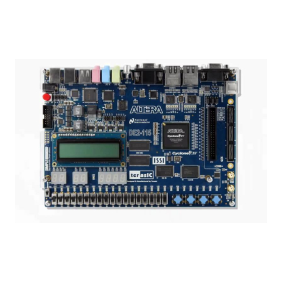
Chapter 2 Introduction of the Altera DE2-115 Board This chapter presents the features and design characteristics of the DE2-115 board. A photograph of the DE2-115 board is shown in Figure 2-1 Figure 2-2. It depicts the layout of the board and indicates the location of the connectors and key components. - Page 9 Figure 2-2 The DE2-115 board (bottom view) The DE2-115 board has many features that allow users to implement a wide range of designed circuits, from simple circuits to various multimedia projects. The following hardware is provided on the DE2-115 board: ...
-
Page 10: Block Diagram Of The De2-115 Board
DE2-115 board. In order to use the DE2-115 board, the user has to be familiar with the Quartus II software. The necessary knowledge can be acquired by reading the tutorials “... - Page 11 Following is more detailed information about the blocks in Figure 2-3: Cyclone IV EP4CE115F29 device 114,480 LEs 432 M9K memory blocks 3,888 Kbits embedded memory 4 PLLs JTAG and AS mode configuration EPCS64 serial configuration device ...
- Page 12 40-pin expansion port o Configurable I/O standards (voltage levels:3.3/2.5/1.8/1.5V) VGA-out connector o VGA DAC (high speed triple DACs) DB9 serial connector for RS-232 port with flow control PS/2 mouse/keyboard Three 50MHz oscillator clock inputs SMA connectors (external clock input/output) ...
-
Page 13: Power-Up The De2-115 Board
Turn the RUN/PROG switch (SW19) on the left edge of the DE2-115 board to RUN position; the PROG position is used only for the AS Mode programming. Recycle the power by turning the red power switch on the DE2-115 board OFF and ON again . At this point you should observe the following: ... - Page 14 You can also connect a microphone to the microphone-in connector on the DE2-115 board; your voice will be mixed with the music playing on the audio player Figure 2-4 The default VGA output pattern...
-
Page 15: De2-115 Control Panel
Chapter 3 DE2-115 Control Panel The DE2-115 board comes with a Control Panel facility that allows users to access various components on the board from a host computer. The host computer communicates with the board through a USB connection. The facility can be used to verify the functionality of components on the board or be used as a debug tool while developing RTL code. - Page 16 LEDs and observing the result on the DE2-115 board. Figure 3-1 The DE2-115 Control Panel 3-2. The “Control Circuit” that The concept of the DE2-115 Control Panel is illustrated in Figure performs the control functions is implemented in the FPGA board. It communicates with the Control Panel window, which is active on the host computer, via the USB Blaster link.
-
Page 17: Controlling The Leds, 7-Segment Displays And Lcd Display
Figure 3-2 The DE2-115 Control Panel concept The DE2-115 Control Panel can be used to light up LEDs, change the values displayed on 7-segment and LCD displays, monitor buttons/switches status, read/write the SDRAM, SRAM, EEPROM and Flash Memory, monitor the status of an USB device, communicate with the PS/2 mouse, output VGA color pattern to VGA monitor, verify functionality of HSMC connector I/Os, communicate with PC via RS-232 interface and read SD Card specification information. - Page 18 Figure 3-4. From the window, directly use the left-right arrows to control the 7-SEG patterns on the DE2-115 board which are updated immediately. Note that the dots of the 7-SEGs are not enabled on DE2-115 board. Figure 3-4 Controlling 7-SEG display...
-
Page 19: Switches And Push-Buttons
Choosing the LCD tab leads to the window in Figure 3-5. Text can be written to the LCD display by typing it in the LCD box then pressing the Set button. Figure 3-5 Controlling the LCD display The ability to set arbitrary values into simple display devices is not needed in typical design activities. -
Page 20: Sdram/Sram/Eeprom/Flash Controller And Program-Mer
The Control Panel can be used to write/read data to/from the SDRAM, SRAM, EEPROM, and Flash chips on the DE2-115 board. As an example, we will describe how the SDRAM may be accessed; the same approach is used to access the SRAM, EEPROM, and Flash. Click on the Memory tab and select “SDRAM”... - Page 21 Figure 3-7 Accessing the SDRAM A 16-bit word can be written into the SDRAM by entering the address of the desired location, specifying the data to be written, and pressing the Write button. Contents of the location can be read by pressing the Read button.
-
Page 22: Usb Monitoring
The Control Panel provides users a USB monitoring tool which monitors the status of the USB devices connected to the USB port on the DE2-115 board. By plugging in a USB device to the USB host port of the board, the device type is displayed on the control window. -
Page 23: Ps/2 Device
The Control Panel provides users a PS/2 monitoring tool which monitors the real-time status of a PS/2 mouse connected to the DE2-115 board. The movement of the mouse and the status of the three buttons will be shown in the graphical and text interface. The mouse movement is translated as a position (x,y) with range from (0,0)~(1023,767). -
Page 24: Sd Card
Choosing the SD Card tab leads to the window in Figure 3-10. Insert an SD Card to the DE2-115 board, and then press the Read button to read the SD Card. The SD Card‟s identification, specification, and file format information will be displayed in the control window. -
Page 25: Vga
Receive terminal window to verify its operation. Figure 3-11 RS-232 Serial Communication DE2-115 Control Panel provides VGA pattern function that allows users to output color pattern to LCD/CRT monitor using the DE2-115 board. Follow the steps below to generate the VGA pattern function:... -
Page 26: Hsmc
HSMC connector. Before running the HSMC loopback verification test, follow the instruction noted under the Loopback Installation section and click on Verify. Please note to turn off the DE2-115 board before the HSMC loopback adapter is installed to prevent any damage to the board. -
Page 27: Ir Receiver
Figure 3-13 HSMC loopback verification test performed under Control Panel From the control panel, we can test the IR receiver on the DE2-115 by sending scan code from a remote controller. Figure 3-14 depicts the IR receiver window when the IR tab is pressed. When the scan code is received, the information will be displayed on the IR Receiver window represented in hexadecimal. -
Page 28: Overall Structure Of The De2-115 Control Panel
Figure 3-14 Testing the IR receiver using remote controller The DE2-115 Control Panel is based on a Nios II SOPC system instantiated in the Cyclone IV E FPGA with software running on the on-chip memory. The software part is implemented in C code;... - Page 29 Figure 3-15 The block diagram of the DE2-115 control panel...
-
Page 30: Using The De2-115 Board
This chapter gives instructions for using the DE2-115 board and describes each of its peripherals. The procedure for downloading a circuit from a host computer to the DE2-115 board is described in the tutorial Quartus II Introduction. This tutorial is found in the DE2_115_tutorials folder on the DE2-115 System CD. - Page 31 The sections below describe the steps used to perform both JTAG and AS programming. For both methods the DE2-115 board is connected to a host computer via a USB cable. Using this connection, the board will be identified by the host computer as an Altera USB Blaster device. The process for installing on the host computer the necessary software device driver that communicates with the USB Blaster is described in the tutorial “Getting Started with Altera’s DE2-115 Board”...
- Page 32 Configure the JTAG programming circuit by setting the RUN/PROG slide switch (SW19) to the RUN position (See Figure 4-4) Connect the supplied USB cable to the USB Blaster port on the DE2-115 board (See Figure 2-1) The FPGA can now be programmed by using the Quartus II Programmer to select a configuration bit stream file with the .sof filename extension...
-
Page 33: Using Push-Buttons And Switches
AS configuration setup. To download a configuration bit stream into the EPCS64 serial configuration device, perform the following steps: Ensure that power is applied to the DE2-115 board. Connect the supplied USB cable to the USB Blaster port on the DE2-115 board (See Figure 4-5) ... - Page 34 Schmitt Trigger Debounced Figure 4-7 Switch debouncing There are also 18 slide switches on the DE2-115 board (See Figure 4-8). These switches are not debounced, and are assumed for use as level-sensitive data inputs to a circuit. Each switch is connected directly to a pin on the Cyclone IV E FPGA.
-
Page 35: Using Leds
Figure 4-8 Connections between the slide switches and Cyclone IV E FPGA There are 27 user-controllable LEDs on the DE2-115 board. Eighteen red LEDs are situated above the 18 Slide switches, and eight green LEDs are found above the push-button switches (the 9th green LED is in the middle of the 7-segment displays). - Page 36 Table 4-1 Pin Assignments for Slide Switches Signal Name FPGA Pin No. Description I/O Standard SW[0] PIN_AB28 Slide Switch[0] Depending on JP7 SW[1] PIN_AC28 Slide Switch[1] Depending on JP7 SW[2] PIN_AC27 Slide Switch[2] Depending on JP7 SW[3] PIN_AD27 Slide Switch[3] Depending on JP7 SW[4] PIN_AB27...
-
Page 37: Using The 7-Segment Displays
LEDG[8] PIN_F17 LED Green[8] 2.5V The DE2-115 Board has eight 7-segment displays. These displays are arranged into two pairs and a group of four, behaving the intent of displaying numbers of various sizes. As indicated in the schematic in Figure 4-10, the seven segments (common anode) are connected to pins on Cyclone IV E FPGA. - Page 38 HEX0[5] PIN_J22 Seven Segment Digit 0[5] Depending on JP7 HEX0[6] PIN_H22 Seven Segment Digit 0[6] Depending on JP7 HEX1[0] PIN_M24 Seven Segment Digit 1[0] Depending on JP7 HEX1[1] PIN_Y22 Seven Segment Digit 1[1] Depending on JP7 HEX1[2] PIN_W21 Seven Segment Digit 1[2] Depending on JP7 HEX1[3] PIN_W22...
-
Page 39: Clock Circuitry
Seven Segment Digit 7[6] 3.3V The DE2-115 board includes one oscillator that produces 50 MHz clock signal. A clock buffer is used to distribute 50 MHz clock signal with low jitter to FPGA. The distributing clock signals are connected to the FPGA that are used for clocking the user logic. The board also includes two SMA connectors which can be used to connect an external clock source to the board or to drive a clock signal out through the SMA connector. -
Page 40: Using The Lcd Module
4-6. Figure 4-12 Connections between the LCD module and Cyclone IV E FPGA *(1): Note the current LCD modules used on DE2-115 boards do not have backlight. Therefore the LCD_BLON signal should not be used in users’ design projects. Table 4-6 Pin Assignments for LCD Module Signal Name FPGA Pin No. -
Page 41: High Speed Mezzanine Card
LCD Back Light ON/OFF 3.3V The DE2-115 development board contains a HSMC interface to provide a mechanism for extending the peripheral-set of a FPGA host board by means of add-on cards. This can address today‟s high speed signaling requirement as well as low-speed device interface support. The HSMC interface support JTAG, clock outputs and inputs, high speed LVDS and single-ended signaling. - Page 42 I/O standard between DE2-115 HSMC connector pins and daughter card system. For example, if the I/O standard of HSMC pins on DE2-115 board is set to 1.8V, a daughter card with 3.3V I/O standard may not work properly on DE2-115 board due to I/O standard mismatch.
- Page 43 Figure 4-14 LVDS interface on HSMC connector and Cyclone IV E FPGA Table 4-9 Pin Assignments for HSMC connector FPGA Pin Signal Name Description I/O Standard HSMC_CLKIN0 PIN_AH15 Depending Dedicated clock input on JP6 HSMC_CLKIN_N1 PIN_J28 Depending LVDS RX or CMOS I/O or differential clock input on JP7 HSMC_CLKIN_N2 PIN_Y28...
- Page 44 on JP7 HSMC_RX_D_N[1] PIN_C27 Depending LVDS RX bit 1n or CMOS I/O on JP7 HSMC_RX_D_N[2] PIN_E26 Depending LVDS RX bit 2n or CMOS I/O on JP7 HSMC_RX_D_N[3] PIN_G26 Depending LVDS RX bit 3n or CMOS I/O on JP7 HSMC_RX_D_N[4] PIN_H26 Depending LVDS RX bit 4n or CMOS I/O on JP7...
- Page 45 HSMC_RX_D_P[7] PIN_M25 Depending LVDS RX bit 7 or CMOS I/O on JP7 HSMC_RX_D_P[8] PIN_R25 Depending LVDS RX bit 8 or CMOS I/O on JP7 HSMC_RX_D_P[9] PIN_T25 Depending LVDS RX bit 9 or CMOS I/O on JP7 HSMC_RX_D_P[10] PIN_U25 Depending LVDS RX bit 10 or CMOS I/O on JP7 HSMC_RX_D_P[11] PIN_L21 Depending...
-
Page 46: Using The Expansion Header
LVDS TX bit 16 or CMOS I/O on JP7 The DE2-115 Board provides one 40-pin expansion header. The header connects directly to 36 pins of the Cyclone IV E FPGA, and also provides DC +5V (VCC5), DC +3.3V (VCC3P3), and two... - Page 47 GND pins. Figure 4-15 shows the I/O distribution of the GPIO connector. The maximum power consumption of the daughter card that connects to GPIO port is shown in Table 4-10. Figure 4-15 GPIO Pin Arrangement Table 4-10 Power Supply of the Expansion Header Supplied Voltage Max.
- Page 48 The voltage level of the I/O pins on the expansion headers can be adjusted to 3.3V, 2.5V, 1.8V, or 1.5V using JP6 (The default value is 3.3V, see Figure 4-17). Because the expansion I/Os are connected to Bank 4 of the FPGA and the VCCIO voltage (VCCIO4) of this bank is controlled by the header JP6, users can use a jumper to select the input voltage of VCCIO4 to 3.3V, 2.5V, 1.8V, and 1.5V to control the voltage level of the I/O pins.
- Page 49 I/O standard between DE2-115 GPIO connector pins and daughter card system. For example, if the I/O standard of GPIO pins on DE2-115 board is set to 1.8V, a daughter card with 3.3V I/O standard may not work properly on the DE2-115 board due to I/O standard mismatch.
- Page 50 Figure 4-19 Using Emulated LVDS on GPIO Table 4-12 Pin Assignments for Expansion Headers Signal Name FPGA Pin No. Description I/O Standard GPIO[0] PIN_AB22 GPIO Connection DATA[0] Depending on JP6 GPIO[1] PIN_AC15 GPIO Connection DATA[1] Depending on JP6 GPIO[2] PIN_AB21 GPIO Connection DATA[2] Depending on JP6 GPIO[3]...
-
Page 51: Using 14-Pin General Purpose I/O Connector
GPIO Connection DATA[35] Depending on JP6 The DE2-115 Board provides 14-pin expansion header. The header connects directly to 7 pins of the Cyclone IV E FPGA, and also provides DC +3.3V (VCC3P3), and six GND pins as shown in Figure 4-20. -
Page 52: Using Vga
Detailed information for using the ADV7123 video DAC is available in its datasheet, which can be found on the manufacturer‟s website, or in the DE2_115_datasheets\VIDEO-DAC folder on the DE2-115 System CD. The pin assignments between the Cyclone IV E FPGA and the ADV7123 are listed in Table 4-16. - Page 53 Note: The RGB data bus on DE2-115 board is 8 bit instead of 10 bit on DE2/DE2-70 board. Figure 4-22 VGA horizontal timing specification Table 4-14 VGA Horizontal Timing Specification VGA mode Horizontal Timing Spec Configuration Resolution(HxV) a(us) b(us) c(us)
-
Page 54: Using The 24-Bit Audio Codec
VGA SYNC 3.3V The DE2-115 board provides high-quality 24-bit audio via the Wolfson WM8731 audio CODEC (Encoder/Decoder). This chip supports microphone-in, line-in, and line-out ports, with a sample rate adjustable from 8 kHz to 96 kHz. The WM8731 is controlled via serial I2C bus interface*, which is connected to pins on the Cyclone IV E FPGA. -
Page 55: Serial Port
I2C_SDA. Because audio chip, TV decoder chip and HSMC share one I2C bus, therefore audio and video chip won’t function correctly. The DE2-115 board uses the ZT3232 transceiver chip and a 9-pin DB9 connector for RS-232 communications. For detailed information on how to use the transceiver, please refer to the datasheet, which is available on the manufacturer‟s website, or in the DE2_115_datasheets\RS-232... -
Page 56: Ps/2 Serial Port
UART_RTS PIN_J13 UART Request to Send 3.3V The DE2-115 board includes a standard PS/2 interface and a connector for a PS/2 keyboard or mouse. Figure 4-25 shows the schematic of the PS/2 circuit. In addition, users can use the PS/2... -
Page 57: Gigabit Ethernet Transceiver
PS2_DAT2 PIN_F5 PS/2 Data (reserved for second PS/2 device) 3.3V The DE2-115 board provides Ethernet support via two Marvell 88E1111 Ethernet PHY chips. The 88E1111 chip with integrated 10/100/1000 Mbps Gigabit Ethernet transceiver support GMII/MII/RGMII/TBI MAC interfaces. Table 4-20 describes the default settings for both chips. - Page 58 You will need to perform a hardware reset after any change for enabling new settings. Table 4-21 Table 4-22 describe the working mode settings for ENET0 PHY (U8) and ENET1 PHY (U9) respectively. In addition, it is dynamically configurable to support 10Mbps, 100Mbps (Fast Ethernet) or 1000Mbps (Gigabit Ethernet) operation using standard Cat 5e UTP cabling.
- Page 59 Table 4-22 Jumper Settings for Working Mode of ENET1 (U9) JP2 Jumper Settings ENET1 PHY Working Mode Short Pins 1 and 2 RGMII Mode Short Pins 2 and 3 MII Mode Table 4-23 Pin Assignments for Fast Ethernet Signal Name FPGA Pin No.
- Page 60 Ethernet clock source 3.3V The DE2-115 board is equipped with an Analog Device ADV7180 TV decoder chip. The ADV7180 is an integrated video decoder that automatically detects and converts a standard analog baseband television signals (NTSC, PAL, and SECAM) into 4:2:2 component video data compatible with the 8-bit ITU-R BT.656 interface standard.
-
Page 61: Tv Decoder
I2C Data 3.3V Although the DE2-115 board does not include a TV encoder chip, the ADV7123 (10-bit high-speed triple ADCs) can be used to implement a professional-quality TV encoder with the digital processing part implemented in the Cyclone IV E FPGA. -
Page 62: Using The Usb Interface
The DE2-115 board provides both USB host and device interfaces using the Philips ISP1362 single-chip USB controller. The host and device controllers are compliant with the Universal Serial Bus Specification Rev. 2.0, supporting data transfer at full-speed (12 Mbit/s) and low-speed (1.5 Mbit/s). -
Page 63: Using Ir
3.3V The DE2-115 provides an infrared remote-control receiver Module (model: IRM-V538N7/TR1), whose datasheet is offered in the DE2_115_datasheets\IR_Receiver folder on DE2-115 system CD. Note that for this all-in-one receiver module, it is only compatible with the 38KHz carrier Standard, with a maximum data rate of about 4kbps for its product information. The accompanied remote controller with an encoding chip of uPD6121G is very suitable of generating expected infrared signals. -
Page 64: Using Sram/Sdram/Flash/Eeprom/Sd Card
3.3V SRAM The DE2-115 board has 2MB SRAM memory with 16-bit data width. Being featured with a maximum performance frequency of about 125MHz under the condition of standard 3.3V single power supply makes it suitable of dealing with high-speed media processing applications that need ultra data throughput. - Page 65 Figure 4-34 Connections between FPGA and SDRAM FLASH The board is assembled with 8MB of flash memory using an 8-bit data bus. The device uses 3.3V CMOS signaling standard. Because of its non-volatile property, it is usually used for storing software binaries, images, sounds or other media.
- Page 66 Many applications use a large external storage device, such as SD Card or CF card, for storing data. The DE2-115 board provides the hardware needed for SD Card access. Users can implement custom controllers to access the SD Card in SPI mode and SD Card 4-bit or 1-bit mode.
- Page 67 Figure 4-37 Connections between FPGA and SD Card Socket Table 4-27 SRAM Pin Assignments Signal Name FPGA Pin No. Description I/O Standard SRAM_ADDR[0] PIN_AB7 SRAM Address[0] 3.3V SRAM_ADDR[1] PIN_AD7 SRAM Address[1] 3.3V SRAM_ADDR[2] PIN_AE7 SRAM Address[2] 3.3V SRAM_ADDR[3] PIN_AC7 SRAM Address[3] 3.3V SRAM_ADDR[4] PIN_AB6...
- Page 68 SRAM_DQ[7] PIN_AF7 SRAM Data[7] 3.3V SRAM_DQ[8] PIN_AD1 SRAM Data[8] 3.3V SRAM_DQ[9] PIN_AD2 SRAM Data[9] 3.3V SRAM_DQ[10] PIN_AE2 SRAM Data[10] 3.3V SRAM_DQ[11] PIN_AE1 SRAM Data[11] 3.3V SRAM_DQ[12] PIN_AE3 SRAM Data[12] 3.3V SRAM_DQ[13] PIN_AE4 SRAM Data[13] 3.3V SRAM_DQ[14] PIN_AF3 SRAM Data[14] 3.3V SRAM_DQ[15] PIN_AG3 SRAM Data[15]...
- Page 69 DRAM_DQ[16] PIN_M8 SDRAM Data[16] 3.3V DRAM_DQ[17] PIN_L8 SDRAM Data[17] 3.3V DRAM_DQ[18] PIN_P2 SDRAM Data[18] 3.3V DRAM_DQ[19] PIN_N3 SDRAM Data[19] 3.3V DRAM_DQ[20] PIN_N4 SDRAM Data[20] 3.3V DRAM_DQ[21] PIN_M4 SDRAM Data[21] 3.3V DRAM_DQ[22] PIN_M7 SDRAM Data[22] 3.3V DRAM_DQ[23] PIN_L7 SDRAM Data[23] 3.3V DRAM_DQ[24] PIN_U5 SDRAM Data[24]...
- Page 70 FL_ADDR[15] PIN_Y10 FLASH Address[15] 3.3V FL_ADDR[16] PIN_AA8 FLASH Address[16] 3.3V FL_ADDR[17] PIN_AH12 FLASH Address[17] 3.3V FL_ADDR[18] PIN_AC12 FLASH Address[18] 3.3V FL_ADDR[19] PIN_AD12 FLASH Address[19] 3.3V FL_ADDR[20] PIN_AE10 FLASH Address[20] 3.3V FL_ADDR[21] PIN_AD10 FLASH Address[21] 3.3V FL_ADDR[22] PIN_AD11 FLASH Address[22] 3.3V FL_DQ[0] PIN_AH8 FLASH Data[0]...
-
Page 71: Chapter 5 De2-115 System Builder
Board malfunction caused by wrong device connections or missing pin counts for connected ends. Performance degeneration because of improper pin assignments. This section will introduce the general design flow to build a project for the DE2-115 board via the DE2-115 System Builder. The general design flow is illustrated in Figure 5-1. -
Page 72: Using De2-115 System Builder
The Quartus II setting file contains information such as FPGA device type, top-level pin assignment, and I/O standard for each user-defined I/O pin. Finally, Quartus II programmer must be used to download SOF file to DE2-115 board using JTAG interface. - Page 73 Input Project Name Input project name as show in Figure 5-3. Project Name: Type in an appropriate name here, it will automatically be assigned as the name of your top-level design entity. Figure 5-3 The DE2-115 Board Type and Project Name...
-
Page 74: System Configuration
If the component is enabled, the DE2-115 System Builder will automatically generate the associated pin assignments including the pin name, pin location, pin direction, and I/O standard. - Page 75 The “Prefix Name” is an optional feature which denotes the prefix pin name of the daughter card assigned in your design. Users may leave this field empty. HSMC Expansion Users can connect HSMC-interfaced daughter cards onto HSMC located on the DE2-115 board shown in Figure 5-6.
- Page 76 The “Prefix Name” is an optional feature that denotes the pin name of the daughter card assigned in your design. Users may leave this field empty. Project Setting Management The DE2-115 System Builder also provides functions to restore default setting, loading a setting, and saving users‟ board configuration file shown in Figure 5-7.
- Page 77 Project Generation When users press the Generate button, the DE2-115 System Builder will generate the corresponding Quartus II files and documents as listed in the Table 5-1: Table 5-1 The files generated by DE2-115 System Builder Filename Description <Project name>.v Top level verilog HDL file for Quartus II <Project name>.qpf...
-
Page 78: Chapter 6 Examples Of Advanced Demonstrations
Project directory: DE2_115_Default Bit stream used: DE2_115_Default.sof or DE2_115_Default.pof Power on the DE2-115 board, with the USB cable connected to the USB Blaster port. If necessary (that is, if the default factory configuration of the DE2-115 board is not currently... -
Page 79: Tv Box Demonstration
You should now be able to observe that the 7-segment displays are displaying a sequence of characters, and the red and green LEDs are flashing. Also, “Welcome to the Altera DE2-115” is shown on the LCD display Optionally connect a VGA display to the VGA D-SUB connector. When connected, the VGA display should show a color picture ... - Page 80 4:3 aspect ratio o Non-progressive video Connect the VGA output of the DE2-115 board to a VGA monitor (both LCD and CRT type of monitors should work) Connect the audio output of the DVD player to the line-in port of the DE2-115 board and connect a speaker to the line-out port.
-
Page 81: Usb Paintbrush
VGA display screen using the USB mouse. The VGA Controller block is integrated into the Altera Avalon bus so that it can be controlled by the Nios II processor. - Page 82 Nios II Workspace: DE2_115_NIOS_HOST_MOUSE_VGA\Software Connect a USB Mouse to the USB Host Connector (type A) of the DE2-115 board Connect the VGA output of the DE2-115 board to a VGA monitor (both LCD and CRT type of monitors should work) ...
-
Page 83: Usb Device
DE2-115 board‟s Philips ISP1362 device. After connecting the DE2-115 board to a USB port on the host computer, a software program has to be executed on the Nios II processor to initialize the Philips ISP1362 chip. Once the software program is successfully executed, the host computer will identify the new device in its USB device list and asks for the associated driver;... - Page 84 Bit stream used: DE2_115_NIOS_DEVICE_LED.sof Nios II Workspace: DE2_115_NIOS_DEVICE_LED\Software Borland C++ Software Driver: DE2_115_NIOS_DEVICE_LED\SW Connect the USB Device connector of the DE2-115 board to the host computer using a USB cable (type AB). Load the bit stream into FPGA(note*) ...
-
Page 85: A Karaoke Machine
Figure 6-6 Setup for the USB device demonstration This demonstration uses the microphone-in, line-in, and line-out ports on the DE2-115 board to create a Karaoke Machine application. The Wolfson WM8731 audio CODEC is configured in the master mode, with which the audio CODEC generates AD/DA serial bit clock (BCK) and the left/right channel clock (LRCK) automatically. - Page 86 Project directory: DE2_115_i2sound Bit stream used: DE2_115_i2sound.sof or DE2_115_i2sound.pof Connect a microphone to the microphone-in port (pink color) on the DE2-115 board Connect the audio output of a music-player, such as an MP3 player or computer, to the line-in port (blue color) on the DE2-115 board ...
-
Page 87: Sd Card Demonstration
Many applications use a large external storage device, such as an SD Card or CF card to store data. The DE2-115 board provides the hardware and software needed for SD Card access. In this demonstration we will show how to browse files stored in the root directory of an SD Card and how to read the file contents of a specific file. - Page 88 LED if it fails to parse the FAT file system or if there is no SD Card found in the SD Card socket of the DE2-115 board. If users press KEY3 of the DE2-115 board,...
- Page 89 Make sure Quartus II and Nios II are installed on your PC. Power on the DE2-115 board. Connect USB Blaster to the DE2-115 board and install USB Blaster driver if necessary. Execute the demo batch file “DE2_115_SD_Card.bat” under the batch file folder, DE2_115_SD_CARD\demo_batch.
-
Page 90: Sd Card Music Player
DE2-115 board. In this demonstration we show how to implement an SD Card Music Player on the DE2-115 board, in which the music files are stored in an SD Card and the board can play the music files via its CD-quality audio DAC circuits. - Page 91 Figure 6-13 shows the hardware block diagram of this demonstration. The system requires a 50 MHz clock provided from the board. The PLL generates a 100MHz clock for Nios II processor and the other controllers except for the audio controller. The audio chip is controlled by the Audio Controller which is a user-defined SOPC component.
- Page 92 7-segment display, and the LEDs. The top and bottom row of the LCD module will display the file name of the music that is played on the DE2-115 board and the value of music volume, respectively. The 7-segment displays will show the elapsed time of the playing music file. The LED will indicate the audio signal strength.
- Page 93 Connect a headset or speaker to the DE2-115 board and you should be able to hear the music played from the SD Card Press KEY3 on the DE2-115 board to play the next music file stored in the SD Card.
-
Page 94: Ps/2 Mouse Demonstration
Figure 6-15 The setup for the SD music player demonstration We offer this simple PS/2 controller coded in Verilog HDL to demonstrate bidirectional communication between PS/2 controller and the device, the PS/2 mouse. You can treat it as a how-to basis and develop your own controller that could accomplish more sophisticated instructions, like setting the sampling rate or resolution, which need to transfer two data bytes. - Page 95 Data transmit from the device to controller After sending an enabling instruction to the PS/2 mouse at stream mode, the device starts to send displacement data out, which consists of 33 bits. The frame data is cut into three similar slices, each of them containing a start bit (always zero) and eight data bits (with LSB first), one parity check bit (odd check), and one stop bit (always one).
- Page 96 Figure 6-16 Waveforms on two lines while communication taking place Demonstration Setup, File Locations, and Instructions Project directory: DE2_115_PS2_DEMO Bit stream used : DE2_115_PS2_DEMO.sof Load the bit stream into FPGA by executing DE2_115_PS2_DEMO\demo_batch\DE2_115_PS2_DEMO.bat Plug in the PS/2 mouse ...
-
Page 97: Ir Receiver Demonstration
6-3) will be displayed on the DE2-115 board. Users only need to point the remote controller to the IR receiver on DE2-115 board and press the key. After the signal being decoded and processed through FPGA, the related information will be displayed on the 7-segment displays in hexadecimal format, which contains Custom Code, Key Code and Inversed Key Code. - Page 98 Figure 6-18 Remote controller Table 6-3 Key code information for each Key on remote controller Key Code Key Code Key Code Key Code 0x0F 0x13 0x10 0x12 0x01 0x02 0x03 0x1A 0x04 0x05 0x06 0x1E 0x07 0x08 0x09 0x1B 0x11 0x00 0x17 0x1F...
- Page 99 After the IR receiver on DE2-115 board receives this frame, it will directly transmit that to FPGA. In this demo, the IP of IR receiver controller is implemented in the FPGA. As Figure 6-20 shows, it includes Code Detector, State Machine, and Shift Register. First, the IR receiver demodulates the signal inputs to Code Detector block .The Code Detector block will check the Lead Code and...
- Page 100 We can apply the IR receiver to many applications, such as integrating to the SD Card Demo, and you can also develop other related interesting applications with it. Demonstration Setup, File Locations, and Instructions Project directory: DE2_115_IR Bit stream used: DE2_115_IR.sof ...
-
Page 101: Music Synthesizer Demonstration
PS/2 Keyboard and a speaker. PS/2 Keyboard is used as the piano keyboard for input. The Cyclone IV E FPGA on the DE2-115 board serves as the Music Synthesizer SOC to generate music and tones. The VGA connected to the DE2-115 board is used to show which key is pressed during the playing of the music. - Page 102 Bit stream used: DE2_115_Synthesizer.sof or DE2-115_Synthesizer.pof Connect a PS/2 Keyboard to the DE2-115 board. Connect the VGA output of the DE2-115 board to a VGA monitor (both LCD and CRT type of monitors should work) Connect the lineout of the DE2-115 board to a speaker.
- Page 103 Table 6-5 Table 6-6 illustrate the usage of the slide switches, push-button switches (KEYs), PS/2 Keyboard. Slide Switches and Push-buttons switches Table 6-5 Usage of the slide switches and push-buttons switches (KEYs) Signal Name Description KEY[0] Reset Circuit KEY[1] Repeat the Demo Music SW[0] OFF: BRASS, ON: STRING...
-
Page 104: Audio Recording And Playing
Figure 6-24 The Setup of the Music Synthesizer Demonstration This demonstration shows how to implement an audio recorder and player using the DE2-115 board with the built-in Audio CODEC chip. This demonstration is developed based on SOPC Builder and Nios II IDE. - Page 105 Figure 6-25 Man-Machine Interface of Audio Recorder and Player Figure 6-26 shows the block diagram of the Audio Recorder and Player design. There are hardware and software parts in the block diagram. The software part stores the Nios II program in SRAM. The software part is built by Nios II IDE in C programming language.
- Page 106 Bit stream used: DE2_115_AUDIO.sof Software Project directory: DE2_115_AUDIO\software\ Connect an Audio Source to the LINE-IN port of the DE2-115 board. Connect a Microphone to MIC-IN port on the DE2-115 board. Connect a speaker or headset to LINE-OUT port on the DE2-115 board.
-
Page 107: Web Server Demonstration
This design example shows a HTTP server using the sockets interface of the NicheStack™ TCP/IP Stack Nios II Edition on MicroC/OS-II to serve web content from the DE2-115 board. The server can process basic requests to serve HTML, JPEG, GIF, PNG, JS, CSS, SWF, ICO files from the Altera read-only .zip file system. - Page 108 Figure 6-27 MII interface MAC Configuration...
- Page 109 Figure 6-28 RGMII interface MAC Configuration In the MAC Options tab (See Figure 6-29), users should set up proper values for the PHY chip 88E1111. The MDIO Module should be included, as it is used to generate a 2.5MHz MDC clock for the PHY chip from the controller's source clock(here a 100MHz clock source is expected) to divide the MAC control register interface clock to produce the MDC clock output on the MDIO interface.
- Page 110 Figure 6-29 MAC Options Configuration Once the Triple-Speed Ethernet IP configuration has been set and necessary hardware connections have been made as shown in Figure 6-30, click on generate.
- Page 111 Figure 6-30 SOPC Builder Figure 6-31 shows the connections for programmable 10/100Mbps Ethernet operation via MII. Figure 6-31 PHY connected to the MAC via MII Figure 6-32 shows the connections for programmable 10/100/1000Mbps Ethernet operation via RGMII.
- Page 112 Figure 6-33. The top block contains the Nios II processor and the necessary hardware to be implemented into the DE2-115 host board. The software device drivers contain the necessary device drivers needed for the Ethernet and other hardware components to work.
- Page 113 NicheStack™ TCP/IP Stack will start to run for Web Server application. Figure 6-34 describes this demo setup and connections on DE2-115. The Nios II processor is running NicheStack™ on the MicroC/OS-II RTOS. Note: your gateway should support DHCP because it uses DHCP protocol to request a valid IP from the Gateway, or else you would need to reconfigure the system library to use static IP assignment.
- Page 114 You will see the brand new DE2-115 webpage on your computer On the web page, you could access the DE2-115 board‟s peripherals from the left sidebar or link to external pages from the right sidebar. Try check some LEDs on the left sidebar and then press send will light up the specified LEDs on board.
- Page 115 Note: Or execute DE2_115_Web_Server\<Web Server Mode-Port Specific>\demo_batch\web_server.bat for downloading .sof and .elf files. Figure 6-34 System Principle Diagram Figure 6-35 Served web page for DE2-115...
-
Page 116: Chapter 7 Appendix
Chapter 7 Appendix Version Change Log V1.0 Initial Version (Preliminary) V1.01 VGA Vertical Timing table correction SDRAM Table reference modification V1.02 Modify Table4-15 Header info. V1.03 Modify section 6.3 demo description Copyright © 2010 Terasic Technologies. All rights reserved.
Need help?
Do you have a question about the DE2-115 and is the answer not in the manual?
Questions and answers