Quectel 5G Module Series Hardware Design
Hide thumbs
Also See for 5G Module Series:
- Hardware design (86 pages) ,
- User manual (47 pages) ,
- User manual (27 pages)

Subscribe to Our Youtube Channel
Related Manuals for Quectel 5G Module Series


Summary of Contents for Quectel 5G Module Series
- Page 1 RM500Q-AE&RM502Q-AE Hardware Design 5G Module Series Version: 1.0 Date: 2021-03-06 Status: Released www.quectel.com...
- Page 2 To the maximum extent permitted by law, Quectel excludes all liability for any loss or damage suffered in connection with the use of the functions and features under development, regardless of whether such loss or damage may have been foreseeable.
- Page 3 RM500Q-AE&RM502Q-AE Hardware Design Copyright The information contained here is proprietary technical information of Quectel. Transmitting, reproducing, disseminating, and editing this document as well as using the content without permission are forbidden. Offenders will be held liable for payment of damages. All rights are reserved in the event of a patent grant or registration of a utility model or design.
-
Page 4: Safety Information
Manufacturers of the cellular terminal should notify users and operating personnel of the following safety information by incorporating these guidelines into all manuals of the product. Otherwise, Quectel assumes no liability for customers’ failure to comply with these precautions. -
Page 5: About The Document
5G Module Series RM500Q-AE&RM502Q-AE Hardware Design About the Document Revision History Version Date Author Description Jared WANG 2020-10-22 Creation of the document /Hank LIU Jared WANG/ 2021-03-06 Hogan SHENG/ First official release /Hank LIU RM500Q-AE&RM502Q-AE_Hardware_Design 4 / 86... -
Page 6: Table Of Contents
5G Module Series RM500Q-AE&RM502Q-AE Hardware Design Contents Safety Information ............................3 About the Document ........................... 4 Contents ............................... 5 Table Index ..............................8 Figure Index ............................... 10 Introduction ............................12 1.1. Introduction ..........................12 1.2. Reference Standard ........................12 1.3. - Page 7 5G Module Series RM500Q-AE&RM502Q-AE Hardware Design 4.3. PCIe Interface ........................... 42 4.3.1. PCIe Operating Mode ....................42 4.3.2. Pin Definition of PCIe ..................... 43 4.3.3. Reference Design for PCIe .................... 44 4.3.4. PCIe Timing ........................45 4.4. PCM Interface ........................... 46 4.5.
- Page 8 5G Module Series RM500Q-AE&RM502Q-AE Hardware Design 6.7. Operating and Storage Temperatures ..................79 Mechanical Dimensions and Packaging ..................80 7.1. Mechanical Dimensions of the Module ..................80 7.2. Top and Bottom Views of the Module ..................81 7.3. M.2 Connector ........................... 82 7.4.
- Page 9 5G Module Series RM500Q-AE&RM502Q-AE Hardware Design Table Index Table 1: Special Mark..........................13 Table 2: Frequency Bands and GNSS Type of RM500Q-AE&RM502Q-AE Module ........ 14 Table 3: Key Features of RM500Q-AE&RM502Q-AE ................15 Table 4: Definition of I/O Parameters ......................20 Table 5: Pin Description ..........................
- Page 10 5G Module Series RM500Q-AE&RM502Q-AE Hardware Design Table 42: (U)SIM 1.8V I/O Requirements ....................76 Table 43: (U)SIM 3.0V I/O Requirements ....................76 Table 44: Electrostatic Discharge Characteristics (Temperature: 25 º C, Humidity: 40 %) ....... 76 Table 45: Absolute Maximum Ratings ....................... 78 Table 46: Operating and Storage Temperatures ..................
- Page 11 5G Module Series RM500Q-AE&RM502Q-AE Hardware Design Figure Index Figure 1: Functional Diagram ........................18 Figure 2: Pin Assignment ........................... 19 Figure 3: DRX Run Time and Current Consumption in Sleep Mode ............26 Figure 4: Sleep Mode Application with USB Remote Wakeup ..............26 Figure 5: Power Supply Limits during Radio Transmission ...............
- Page 12 5G Module Series RM500Q-AE&RM502Q-AE Hardware Design Figure 42: Tray Packaging Procedure ....................... 83 RM500Q-AE&RM502Q-AE_Hardware_Design 11 / 86...
-
Page 13: Introduction
5G Module Series RM500Q-AE&RM502Q-AE Hardware Design Introduction 1.1. Introduction The hardware design defines RM500Q-AE and RM502Q-AE and describes the air and hardware interfaces which are connected to customers’ applications. This document helps you quickly understand the interface specifications, electrical and mechanical details, as well as other related information of RM500Q-AE and RM502Q-AE. -
Page 14: Special Mark
5G Module Series RM500Q-AE&RM502Q-AE Hardware Design 1.3. Special Mark Table 1: Special Mark Mark Definition When an asterisk (*) is used after a function, feature, interface, pin name, AT command, or argument, it indicates that the function, feature, interface, pin name, AT command, or argument is under development and currently not supported, unless otherwise specified. -
Page 15: Product Concept
5G Module Series RM500Q-AE&RM502Q-AE Hardware Design Product Concept 2.1. General Description RM500Q-AE and RM502Q-AE are 5G NR/LTE-FDD/LTE-TDD/WCDMA wireless communication modules with receive diversity. They provide data connectivity on 5G NR SA and NSA, LTE-FDD, LTE-TDD, DC-HSDPA, HSPA+, HSDPA, HSUPA and WCDMA networks. They are standard M.2 Key-B WWAN modules. -
Page 16: Key Features
5G Module Series RM500Q-AE&RM502Q-AE Hardware Design The module can be applied to the following fields: ⚫ Rugged tablet PC and laptop computer ⚫ Remote monitor system ⚫ Smart metering system ⚫ Wireless CPE ⚫ Smart TV ⚫ Outdoor live devices ⚫... - Page 17 5G Module Series RM500Q-AE&RM502Q-AE Hardware Design ⚫ 5G NR bands: Class 3 (23 dBm ± 2 dB) ⚫ 5G NR n41/n77/n78/n79 bands HPUE: Class 2 (26 dBm +2/-3 dB) ⚫ Transmitting Power LTE bands: Class 3 (23 dBm ± 2 dB) ⚫...
- Page 18 5G Module Series RM500Q-AE&RM502Q-AE Hardware Design ⚫ Rx-diversity Supports 5G NR/LTE/WCDMA Rx-diversity ⚫ Protocol: NMEA 0183 GNSS Features ⚫ Data Update Rate: 1 Hz ⚫ Antenna Interfaces ANT0, ANT1, ANT2, and ANT3_GNSSL1 ⚫ Compliant with 3GPP TS 27.007 and 3GPP TS 27.005 AT Commands ⚫...
-
Page 19: Evaluation Board
RM500Q-AE&RM502Q-AE Hardware Design 2.3. Evaluation Board To help you develop applications conveniently with the module, Quectel supplies an evaluation board (PCIe Card EVB), a USB to RS-232 converter cable, a USB type-B cable, antennas, and other peripherals to control or test the module. For more details, please refer to document [2]. -
Page 20: Pin Assignment
5G Module Series RM500Q-AE&RM502Q-AE Hardware Design 2.5. Pin Assignment The following figure shows the pin assignment of the module. The top side contains the antenna connectors. Pin Name Pin Name CONFIG_2 CONFIG_1 AP2SDX_STATUS RESET# USIM1_DET RFFE_VIO_1V8 COEX_TXD PIN75 ANTCTL2 PIN74... -
Page 21: Pin Description
5G Module Series RM500Q-AE&RM502Q-AE Hardware Design 2.6. Pin Description Table 4: Definition of I/O Parameters Type Description Analog Input Analog Output Analog Input/Output Digital Input Digital Output Digital Input/Output Open Drain Power Input Power Output Pull Up Pull Down The following table shows the pin definition and description of the module. - Page 22 5G Module Series RM500Q-AE&RM502Q-AE Hardware Design Ground Turn on/off the module. max = 4.4 V Internally pulled FULL_CARD_ DI, PD High level: Turn on min = 1.19 V down with a 100 POWER_OFF# kΩ resistor. Low level: Turn off max = 0.2 V USB 2.0 differential data...
- Page 23 5G Module Series RM500Q-AE&RM502Q-AE Hardware Design Ground PCM_SYNC DIO, PD PCM data frame sync 1.8 V USB 3.1 super-speed USB_SS_TX_M transmit (-) USIM1_VDD USIM1_RST DO, PD (U)SIM card reset 1.8/3.0 V USB 3.1 super-speed USB_SS_TX_P transmit (+) USIM1_VDD USIM1_CLK DO, PD (U)SIM clock 1.8/3.0 V...
- Page 24 5G Module Series RM500Q-AE&RM502Q-AE Hardware Design Active LOW Ground PCIe clock request. PCIE_CLKREQ_N DO, OD Active LOW PCIE_REFCLK_M PCIe reference clock (-) PCIe wake up PCIE_WAKE_N DO, OD Active LOW PCIE_REFCLK_P PCIe reference clock (+) Used for external MIPI RFFE_CLK DO, PD 1.8 V...
- Page 25 CONFIG_2 Not connected internally NOTES If this function is required, please contact Quectel for more details. 、 This pin is pulled LOW by default, and will be internally pulled up to 1.8 V by software configuration only when (U)SIM hot-plug is enabled by AT+QSIMDET.
-
Page 26: Operating Characteristics
5G Module Series RM500Q-AE&RM502Q-AE Hardware Design Operating Characteristics 3.1. Operating Modes The table below briefly summarizes the various operating modes of RM500Q-AE and RM502Q-AE. Table 6: Overview of Operating Modes Mode Details Software is active. The module has registered on the network, and it Idle is ready to send and receive data. - Page 27 5G Module Series RM500Q-AE&RM502Q-AE Hardware Design DRX OFF Run Time Figure 3: DRX Run Time and Current Consumption in Sleep Mode The following part of this section presents the power saving procedure and sleep mode of the module. If the host supports USB suspend/resume and remote wakeup function, the following two conditions must be met to make the module enter sleep mode.
-
Page 28: Airplane Mode
5G Module Series RM500Q-AE&RM502Q-AE Hardware Design 3.1.2. Airplane Mode The module provides a W_DISABLE1# pin to disable or enable airplane mode through hardware operation. See Chapter 4.5.1 for more details. 3.2. Communication Interface with a Host The module supports to communicate through both USB and PCIe interfaces, respectively referring to the... -
Page 29: Power Supply
5G Module Series RM500Q-AE&RM502Q-AE Hardware Design 3.3. Power Supply The following table shows pin definition of VCC pins and ground pins. Table 7: Definition of VCC and GND Pins Pin Name Description DC Characteristics 3.135–4.4 V 2, 4, 70, 72, 74 Power supply 3.7 V typical DC supply... -
Page 30: Reference Design For Power Supply
5G Module Series RM500Q-AE&RM502Q-AE Hardware Design Module VCC (3.7 V Typ.) 2, 4 220 μF 1 μF 100 nF 33 pF 10 pF 3, 5, 11 70, 72, 74 220 μF 1 μF 5.1 V 100 nF 33 pF 10 pF... -
Page 31: Monitor The Power Supply
5G Module Series RM500Q-AE&RM502Q-AE Hardware Design NOTE To avoid damages to the internal flash, DON'T cut off the power supply before the module is completely turned off by pulling down FULL_CARD_POWER_OFF# pin for more than 7 s, and DON'T cut off power supply directly when the module is working. - Page 32 5G Module Series RM500Q-AE&RM502Q-AE Hardware Design It is recommended to use a host GPIO to control FULL_CARD_POWER_OFF#. A simple reference circuit is illustrated in the following figure. Host Module 1.8 V or 3.3 V FULL_CARD_POWER_OFF# GPIO PMIC 100k NOTE: The voltage of pin 6 should be no less than 1.19V when it is at HIGH level.
-
Page 33: Turn Off
5G Module Series RM500Q-AE&RM502Q-AE Hardware Design 68 ms Module system turn-on time. turn-on 20 s 22 s Module system booting time. booting Network registering time related to network CSQ. registering 3.5. Turn off 3.5.1. Turn off the Module through FCPO# For the design that turns on the module with a host GPIO, when the power is supplied to VCC, driving FULL_CARD_POWER_OFF# pin LOW (≤... -
Page 34: Turn Off The Module Through At Command
5G Module Series RM500Q-AE&RM502Q-AE Hardware Design 3.5.2. Turn off the Module through AT Command It is also a safe method to turn off the module by AT+QPOWD command. For more details about the command, see document [3]. The module is designed to be turned on with a host GPIO. Pull down FULL_CARD_POWER_OFF# pin after the module’s USB/PCIe is removed. -
Page 35: Reset
5G Module Series RM500Q-AE&RM502Q-AE Hardware Design 3.6. Reset RESET# is an asynchronous and active LOW signal (1.5 V logic level). Whenever this pin is active, the module will immediately enter Power On Reset (POR) condition. Please note that triggering the RESET# signal will lead to loss of all data in the modem and removal of system drivers. - Page 36 5G Module Series RM500Q-AE&RM502Q-AE Hardware Design Module VDD 1.5V 100k RESET# PMIC 33 pF 250-600 ms NOTE: The capacitor C1 is recommended to be less than 47 pF. Figure 13: Reference Circuit of RESET# with a Button The timing of reset scenario is illustrated in the following figure.
-
Page 37: Application Interfaces
5G Module Series RM500Q-AE&RM502Q-AE Hardware Design Application Interfaces The physical connections and signal levels of RM500Q-AE and RM502Q-AE comply with the PCI Express M.2 specification. This chapter mainly describes the definition and application of the following interfaces/pins of the module: ⚫... -
Page 38: U)Sim Hot-Plug
5G Module Series RM500Q-AE&RM502Q-AE Hardware Design USIM1_DET DI, PU (U)SIM1 card hot-plug detect Internally pulled up to 1.8 V NOTE This pin is pulled LOW by default, and will be internally pulled up to 1.8 V by software configuration only when (U)SIM hot-plug is enabled by AT+QSIMDET. -
Page 39: Normally Closed (U)Sim Card Connector
5G Module Series RM500Q-AE&RM502Q-AE Hardware Design NOTES Hot-plug function is invalid if the configured value of <insert_level> is inconsistent with hardware design. Hot-plug function setting takes effect after the module is restarted. The underlined value is the default parameter value. -
Page 40: U)Sim Card Connector Without Hot-Plug
5G Module Series RM500Q-AE&RM502Q-AE Hardware Design USIM1_DET will change from high to low level; when the (U)SIM card is removed, USIM1_DET will change from low to high level. ⚫ When the (U)SIM is absent, CD1 is open from CD2 and USIM1_DET is at high level. -
Page 41: U)Sim Design Notices
5G Module Series RM500Q-AE&RM502Q-AE Hardware Design 4.1.6. (U)SIM Design Notices To enhance the reliability and availability of the (U)SIM card in applications, please follow the criteria below in (U)SIM circuit design. ⚫ Place the (U)SIM card connector as close to the module as possible. Keep the trace length less than 200 mm. - Page 42 5G Module Series RM500Q-AE&RM502Q-AE Hardware Design USB_SS_RX_M USB 3.1 super-speed receive (-) USB_SS_RX_P USB 3.1 super-speed receive (+) For more details about the USB 3.1 & 2.0 specifications, please visit http://www.usb.org/home. The USB 2.0 interface is recommended to be reserved for firmware upgrade in designs. The following figure shows a reference circuit of USB 3.1 &...
-
Page 43: Pcie Interface
5G Module Series RM500Q-AE&RM502Q-AE Hardware Design ⚫ Junction capacitance of the ESD protection device might cause influences on USB data lines, so you should pay attention to the selection of the device. Typically, the stray capacitance should be less than 1.0 pF for USB 2.0, and less than 0.15 pF for USB 3.1. -
Page 44: Pin Definition Of Pcie
5G Module Series RM500Q-AE&RM502Q-AE Hardware Design PCIe RC mode. NOTES The underlined value is the default parameter value. For more details about the command, see document [3]. 4.3.2. Pin Definition of PCIe The following table shows the pin definition of PCIe interface. -
Page 45: Reference Design For Pcie
5G Module Series RM500Q-AE&RM502Q-AE Hardware Design 4.3.3. Reference Design for PCIe The following figure shows a reference circuit for the PCIe interface. Host Module R4 0 Ω PCIE_REFCLK_P PCIE_REFCLK_P R5 0 Ω PCIE_REFCLK_M PCIE_REFCLK_M PCIE_RX_P C3 220 nF PCIE_TX_P PCIE_RX_M... -
Page 46: Pcie Timing
5G Module Series RM500Q-AE&RM502Q-AE Hardware Design 4.3.4. PCIe Timing Figure 20: PCIe Power-up Timing of M.2 Specification Table 17: PCIe Power-up Timing of M.2 Specification Symbol Min. Typ. Max. Comment 50 ms Power valid to PERST# Input inactive PVPGL 100 μs... -
Page 47: Pcm Interface
5G Module Series RM500Q-AE&RM502Q-AE Hardware Design Table 18: PCIe Turn-on Timing of the Module Symbol Min. Typ. Max. Comment 0 ms 20 ms Module power-on time depending on the host. power-on 68 ms Module system turn on time. turn-on 90 ms 100 ms PCIe clock request. - Page 48 5G Module Series RM500Q-AE&RM502Q-AE Hardware Design 125 μs PCM_CLK PCM_SYNC PCM_DOUT PCM_DIN Figure 22: Primary Mode Timing 125 μs PCM_CLK PCM_SYNC PCM_DOUT PCM_DIN Figure 23: Auxiliary Mode Timing The following table shows the pin definition of PCM interface which can be applied to audio codec design.
-
Page 49: Control And Indication Interfaces
5G Module Series RM500Q-AE&RM502Q-AE Hardware Design PCM_SYNC DIO, PD PCM data frame sync 1.8 V The clock and mode can be configured by AT command, and the default configuration is slave mode using short frame synchronization format with 2048 kHz PCM_CLK and 8 kHz PCM_SYNC. See document [3] for details about AT+QDAI command. -
Page 50: W_Disable2
5G Module Series RM500Q-AE&RM502Q-AE Hardware Design Table 21: RF Function Status W_DISABLE1# Level AT Commands RF Function Status AT+CFUN=1 Enabled High Level AT+CFUN=0 Disabled AT+CFUN=4 AT+CFUN=0 Low Level AT+CFUN=1 Disabled AT+CFUN=4 4.5.2. W_DISABLE2# The module provides a W_DISABLE2# pin to disable or enable the GNSS function. The W_DISABLE2# pin is pulled up by default. -
Page 51: Wwan_Led
5G Module Series RM500Q-AE&RM502Q-AE Hardware Design A simple level shifter based on diodes is used on W_DISABLE1# pin and W_DISABLE2# pin which are pulled up to a 1.8 V voltage in the module, as shown in the following figure. So, the control signals (GPIO) of the host device could be at 1.8 V or 3.3 V voltage level. -
Page 52: Wake_On_Wan
5G Module Series RM500Q-AE&RM502Q-AE Hardware Design The following table shows the RF status indicated by WWAN_LED#. Table 23: Network Status Indications of WWAN_LED# WWAN_LED# Level Description Low Level (LED ON) RF function is turned on RF function is turned off if any of the following occurs: ⚫... -
Page 53: Dpr
5G Module Series RM500Q-AE&RM502Q-AE Hardware Design 4.5.5. DPR* The module provides the DPR (Dynamic Power Reduction) pin for body SAR (Specific Absorption Rate) detection. The signal is sent from a host system proximity sensor to the module to provide an input trigger, which will reduce the output power in radio transmission. -
Page 54: Antenna Tuner Control Interface
ANTCTL2* DO, PD 1.8 V NOTE If this function is required, please contact Quectel for more details. 4.8. Configuration Pins The module provides four configuration pins, which are defined as below. Table 28: Configuration Pins List of M.2 Specification Config_0... - Page 55 5G Module Series RM500Q-AE&RM502Q-AE Hardware Design Table 29: Configuration Pins of the Module Pin No. Pin Name Description CONFIG_0 Not connected internally CONFIG_1 Connected to GND internally CONFIG_2 Not connected internally CONFIG_3 Not connected internally The following figure shows a reference circuit of these four pins.
-
Page 56: Rf Characteristics
5G Module Series RM500Q-AE&RM502Q-AE Hardware Design RF Characteristics This chapter mainly describes RF characteristics of the module. 5.1. Cellular Antenna Interfaces 5.1.1. Pin Definition The pin definition of antenna interfaces is shown below. Table 30: RM500Q-AE&RM502Q-AE Pin Definition of Antenna Interfaces... -
Page 57: Port Mapping
5G Module Series RM500Q-AE&RM502Q-AE Hardware Design NOTES NR TRX1 = TX MIMO + PRX MIMO; NR DRX1 = DRX MIMO. UHB frequency range: 3400–3800 MHz. 5.1.2. Port Mapping Table 31: RM500Q-AE & RM502Q-AE Antenna Mapping 5G NR n77/n78 Antenna WCDMA... - Page 58 5G Module Series RM500Q-AE&RM502Q-AE Hardware Design – PCS (1900) 1850–1910 1930–1990 – DCS (1800) 1710–1785 1805–1880 – – 1710–1755 2110–2155 – Cell (850) 824–849 869–894 – – – JCELL (800) 830–840 875–885 – – IMT-E (2600) 2500–2570 2620–2690 – EGSM (950) 880–915...
-
Page 59: Receiving Sensitivity
5G Module Series RM500Q-AE&RM502Q-AE Hardware Design – – 1710–1780 2110–2200 – – 663–698 617–652 – – – 3300–4200 3300–4200 – – – 3300–3800 3300–3800 – – – 4400–5000 4400–5000 5.1.4. Receiving Sensitivity The following tables show conducted receiving sensitivity of RM500Q-AE and RM502Q-AE. - Page 60 5G Module Series RM500Q-AE&RM502Q-AE Hardware Design LTE-FDD B13 (10 MHz) -100.0 -101.5 -102.5 -93.3 dBm LTE-FDD B14 (10 MHz) -100.0 -101.2 -102.5 -93.3 dBm LTE-FDD B18 (10 MHz) -98.7 -101.0 -102.0 -96.3 dBm LTE-FDD B19 (10 MHz) -99.0 -101.2 -102.1 -96.3 dBm...
- Page 61 5G Module Series RM500Q-AE&RM502Q-AE Hardware Design 5G NR-FDD n7 (20 MHz) -93.5 -96.5 -92.0 dBm (SCS: 15 kHz) 5G NR-FDD n8 (20 MHz) -95.0 -97.0 -98.5 -90.0dBm (SCS: 15 kHz) 5G NR-FDD n12 (15 MHz) -95.0 -98.0 -99.5 -84.0 dBm...
-
Page 62: Output Power
5G Module Series RM500Q-AE&RM502Q-AE Hardware Design 5.1.5. Output Power The following table shows the RF output power of the module. Table 34: Cellular Output Power Mode Frequency Max. Min. WCDMA WCDMA bands 24 dBm +1/-3 dB (Class 3) < -50 dBm LTE bands 23 dBm ±... -
Page 63: Gnss Frequency
5G Module Series RM500Q-AE&RM502Q-AE Hardware Design 5.2.2. GNSS Frequency Table 35: GNSS Frequency Type Frequency Unit GPS/Galileo/QZSS 1575.42 ± 1.023 (L1) Galileo 1575.42 ± 2.046 (E1) QZSS 1575.42 (L1) GLONASS 1597.5–1605.8 BeiDou/COMPASS 1561.098 ± 2.046 NOTES to 50 Ω. Keep the characteristic impedance for the trace of GNSS antenna (ANT3_GNSSL1) π-type... -
Page 64: Antenna Connectors
5G Module Series RM500Q-AE&RM502Q-AE Hardware Design Autonomous 22.55 Warm start @ open sky XTRA enabled 2.02 Autonomous 1.33 Hot start @ open sky XTRA enabled 1.47 Accuracy Autonomous CEP-50 (GNSS) @ open sky NOTES Tracking sensitivity: the minimum GNSS signal power at which the module can maintain lock (keep positioning for at least 3 minutes continuously). -
Page 65: Antenna Connector Size
5G Module Series RM500Q-AE&RM502Q-AE Hardware Design ANT0 ANT1 ANT2 ANT3_GNSSL1 Figure 29: RM502Q-AE Antenna Connectors 5.3.2. Antenna Connector Size RM500Q-AE and RM502Q-AE are mounted with standard 2 mm × 2 mm receptacle antenna connectors for convenient antenna connection. The antenna connector’s PN is IPEX 20579-001E, and the connector... -
Page 66: Antenna Connector Installation
5G Module Series RM500Q-AE&RM502Q-AE Hardware Design Table 37: Major Specifications of the RF Connector Item Specification Nominal Frequency Range DC to 6 GHz 50 Ω Nominal Impedance Temperature Rating -40 ° C to +85 ° C Meet the requirements of: Voltage Standing Wave Ratio (VSWR) Max 1.3 (DC–3 GHz) - Page 67 5G Module Series RM500Q-AE&RM502Q-AE Hardware Design The following figure illustrates the connection between the receptacle RF connector on the module and the mating plug using a Ø 0.81 mm coaxial cable. Figure 32: Connection Between RF Connector and Mating Plug Using Ø 0.81 mm Coaxial Cable The following figure illustrates the connection between the receptacle RF connector on the module and the mating plug using a Ø...
-
Page 68: Recommended Rf Connector Installation
5G Module Series RM500Q-AE&RM502Q-AE Hardware Design 5.3.4. Recommended RF Connector Installation 5.3.4.1. Assemble Coaxial Cable Plug Manually The illustration for plugging in a coaxial cable plug is shown below, θ = 90° is acceptable, while θ ≠ 90° is not. -
Page 69: Assemble Coaxial Cable Plug With Jig
5G Module Series RM500Q-AE&RM502Q-AE Hardware Design The illustration of pulling out the coaxial cable plug is shown below, θ = 90° is acceptable, while θ ≠ 90° is not. Figure 35: Pull out a Coaxial Cable Plug 5.3.4.2. Assemble Coaxial Cable Plug with Jig The pictures of installing the coaxial cable plug with a jig is shown below, θ... -
Page 70: Recommended Manufacturers Of Rf Connector And Cable
5G Module Series RM500Q-AE&RM502Q-AE Hardware Design 5.3.5. Recommended Manufacturers of RF Connector and Cable RF connecters and cables by I-PEX are recommended. For more details, visit https://www.i-pex.com. 5.4. Antenna Requirements The following table shows the requirements on WCDMA, LTE, 5G NR antenna and GNSS antennas. -
Page 71: Electrical Characteristics And Reliability
5G Module Series RM500Q-AE&RM502Q-AE Hardware Design Electrical Characteristics and Reliability 6.1. Power Supply Requirements The typical input voltage of the module is 3.7 V, the following table shows the power supply requirements of the module. Table 39: Power Supply Requirements... - Page 72 5G Module Series RM500Q-AE&RM502Q-AE Hardware Design LTE-TDD @ DRX = 0.64s, USB Suspend 5.803 WCDMA @ Paging Frame = 64 31.06 WCDMA @ Paging Frame = 64, USB Active 52.42 LTE-FDD @ DRX = 0.64 s 32.93 Idle state LTE-FDD @ DRX = 0.64 s, USB Active 54.77...
- Page 73 5G Module Series RM500Q-AE&RM502Q-AE Hardware Design LTE-FDD B3 CH1575 @ 23 dBm LTE-FDD B4 CH2175 @ 23 dBm LTE-FDD B5 CH2525 @ 23 dBm LTE-FDD B7 CH3100 @ 23 dBm LTE-FDD B8 CH3625 @ 23 dBm LTE-FDD B12(B17) CH5095 @ 23 dBm...
- Page 74 5G Module Series RM500Q-AE&RM502Q-AE Hardware Design 5G NR-TDD n41 CH501204 @ 26 dBm 5G NR-TDD n41 CH518598 @ 26 dBm 5G NR-TDD n41 CH535998 @ 26 dBm 5G NR-TDD n77 CH620668 @ 26 dBm 5G NR-TDD n77 CH650000 @ 26 dBm...
- Page 75 5G Module Series RM500Q-AE&RM502Q-AE Hardware Design 5G NR-FDD n7 CH531000 @ 23 dBm 5G NR-FDD n7 CH537000 @ 23 dBm 5G NR-FDD n8 CH186000 @ 23 dBm 5G NR-FDD n8 CH188500 @ 23 dBm 5G NR-FDD n8 CH191000 @ 23 dBm...
-
Page 76: Digital I/O Characteristic
5G Module Series RM500Q-AE&RM502Q-AE Hardware Design 5G NR-TDD n48 CH646333@ 23 dBm 5G NR-FDD n66 CH423000 @ 23 dBm 5G NR-FDD n66 CH429000 @ 23 dBm 5G NR-FDD n66 CH435000 @ 23 dBm 5G NR-FDD n71 CH124400 @ 23 dBm... -
Page 77: Electrostatic Discharge
5G Module Series RM500Q-AE&RM502Q-AE Hardware Design Table 42: (U)SIM 1.8V I/O Requirements Parameter Description Min. Max. Unit USIM1_VDD Power supply 1.65 1.95 Input high voltage 0.7 × USIM1_VDD USIM1_VDD + 0.3 Input low voltage -0.3 0.2 × USIM1_VDD Output high voltage 0.8 ×... -
Page 78: Thermal Dissipation
5G Module Series RM500Q-AE&RM502Q-AE Hardware Design Other Interfaces ± 0.5 ± 1 6.5. Thermal Dissipation RM500Q-AE and RM502Q-AE are designed to work in an extended temperature range. To achieve a maximum performance while working under extended temperatures or extreme conditions (such as with maximum power or data rate) for a long time, it is strongly recommended to add a thermal pad or other thermally conductive compounds between the module and the main PCB for thermal dissipation. -
Page 79: Absolute Maximum Ratings
5G Module Series RM500Q-AE&RM502Q-AE Hardware Design Other measures to enhance heat dissipation performance are listed as follows: ⚫ Add as many ground vias as possible on the PCB. ⚫ Maximize airflow over/around the module. ⚫ Place the module away from other heating sources. -
Page 80: Operating And Storage Temperatures
5G Module Series RM500Q-AE&RM502Q-AE Hardware Design 6.7. Operating and Storage Temperatures Table 46: Operating and Storage Temperatures Parameter Min. Typ. Max. Unit Operating Temperature Range º C Extended Temperature Range º C Storage temperature Range º C NOTES To meet this operating temperature range, you need to ensure effective thermal dissipation, for example, by adding passive or active heatsinks, heat pipes, vapor chambers, etc. -
Page 81: Mechanical Dimensions And Packaging
5G Module Series RM500Q-AE&RM502Q-AE Hardware Design Mechanical Dimensions and Packaging This chapter mainly describes mechanical dimensions and packaging specifications of RM500Q-AE and RM502Q-AE. All dimensions are measured in mm, and the tolerances are ± 0.05 mm unless otherwise specified. 7.1. Mechanical Dimensions of the Module Figure 38: Mechanical Dimensions of the Module (Unit: mm) RM500Q-AE&RM502Q-AE_Hardware_Design... -
Page 82: Top And Bottom Views Of The Module
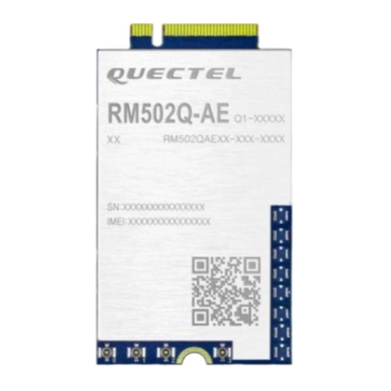
Figure 40: RM502Q-AE Top View and Bottom View NOTE Images above are for illustration purpose only and may differ from the actual module. For authentic appearance and label, please refer to the module received from Quectel. RM500Q-AE&RM502Q-AE_Hardware_Design 81 / 86... -
Page 83: Connector
5G Module Series RM500Q-AE&RM502Q-AE Hardware Design 7.3. M.2 Connector The module adopts a standard PCI Express M.2 connector which compiles with the directives and standards listed in the PCI Express M.2 Specification. 7.4. Packaging The modules are packaged in trays. The following figure shows the tray size. - Page 84 5G Module Series RM500Q-AE&RM502Q-AE Hardware Design Figure 42: Tray Packaging Procedure RM500Q-AE&RM502Q-AE_Hardware_Design 83 / 86...
-
Page 85: Appendix References
5G Module Series RM500Q-AE&RM502Q-AE Hardware Design Appendix References Table 47: Related Documents Document Name Description CA and EN-DC features of RM500Q-AE Quectel_RM50xQ-AE_CA&EN-DC_Features and RM502Q-AE modules. Quectel_PCIe_Card_EVB_User_Guide PCIe card EVB user guide. Quectel_RG50xQ&RM5xxQ_Series_AT_Commands_ The AT command manual for RG50xQ Manual series and RM5xxQ series. - Page 86 5G Module Series RM500Q-AE&RM502Q-AE Hardware Design Dynamic Power Reduction Discontinuous Reception (Chapter 3.1.1, Chapter 6.2) Diversity Reception (Chapter 5) Electrostatic Discharge EndPoint Envelope Tracking Frequency Division Duplexing GLONASS Global Navigation Satellite System (Russia) GNSS Global Navigation Satellite System Global Positioning System...
- Page 87 5G Module Series RM500Q-AE&RM502Q-AE Hardware Design PCIe Peripheral Component Interconnect Express Pulse Code Modulation Protocol Data Unit Point-to-Point Protocol Root Complex Radio Frequency RFFE RF Front-End Receive Specific Absorption Rate Sub-carrier Spacing Short Message Service Transmission Control Protocol Transmit UART Universal Asynchronous Receiver &...
Need help?
Do you have a question about the 5G Module Series and is the answer not in the manual?
Questions and answers