Quectel L76 Hardware Design
Hide thumbs
Also See for L76:
- User manual (32 pages) ,
- Reference design (9 pages) ,
- Command manual (29 pages)

Related Manuals for Quectel L76


Summary of Contents for Quectel L76
- Page 1 L76&L76-L Hardware Design GNSS Module Series Version: 3.2 Date: 2021-08-16 Status: Released...
- Page 2 To the maximum extent permitted by law, Quectel excludes all liability for any loss or damage suffered in connection with the use of the functions and features under development, regardless of whether such loss or damage may have been foreseeable.
- Page 3 GNSS Module Series Copyright The information contained here is proprietary technical information of Quectel. Transmitting, reproducing, disseminating and editing this document as well as using the content without permission are forbidden. Offenders will be held liable for payment of damages. All rights are reserved in the event of a patent grant or registration of a utility model or design.
-
Page 4: Safety Information
Manufacturers of the terminal should notify users and operating personnel of the following safety information by incorporating these guidelines into all product manuals. Otherwise, Quectel assumes no liability for customers’ failure to comply with these precautions. -
Page 5: About The Document
2015-11-11 Added the information about L76G module. Deleted the information about L76G module. 2016-04-26 Added the information about L76-L module. 3. Added chapter 3.9: EPO Data Service 2016-05-18 Added the description of I2C about L76-L module. L76&L76-L_Hardware_Design 4 / 59... - Page 6 GNSS Module Series Deleted the information about L76B; Added the information about the L76-L(L) module; Updated the name of PIN2 from TXD1 to TXD; Updated the name of PIN3 from RXD1 to RXD; Updated the name of PIN9 from RESET to RESET_N;...
-
Page 7: Table Of Contents
Standby Mode ........................ 24 3.3.3. Backup Mode ......................... 25 3.3.4. Periodic Mode ........................ 26 3.3.5. GLP Mode ........................27 AlwaysLocate™ Mode ....................28 3.3.6. 3.4. Power-Up Sequence ....................... 29 3.5. Power-Down Sequence ......................30 Application Interfaces ........................31 L76&L76-L_Hardware_Design 6 / 59... - Page 8 Top and Bottom Views ......................49 Product Handling ..........................50 8.1. Packaging ..........................50 8.1.1. Tapes ..........................50 8.1.2. Reels ..........................51 8.2. Storage ............................ 51 8.3. Manufacturing and Soldering ....................52 Labelling Information ........................55 10 Appendix References ........................56 L76&L76-L_Hardware_Design 7 / 59...
- Page 9 Table 7: Absolute Maximum Ratings ......................45 Table 8: Recommended Operating Conditions ..................46 Table 9: Reel Packaging ..........................51 Table 10: Recommended Thermal Profile Parameters ................53 Table 11: Related Documents ........................56 Table 12: Terms and Abbreviations ......................56 L76&L76-L_Hardware_Design 8 / 59...
- Page 10 Figure 12: UART Interface Reference Design ................... 31 Figure 13: RS-232 Level Shift Circuit ......................32 Figure 14: I2C Interface Reference Design for L76-L Module ..............33 Figure 15: 1PPS & NMEA Timing ......................34 Figure 16: Reference OC Circuit for Module Reset ................... 34 Figure 17: Reset Sequence ........................
-
Page 11: Product Description
The embedded flash memory provides the capacity for storing user-specific configurations and future firmware updates. ⚫ L76 and L76-L, the standard I/O voltage variants, have 2.7–2.9 V I/O voltage; L76-L(L), the low I/O voltage variant has a 1.7–1.9 V I/O voltage. ⚫... -
Page 12: Features
GNSS Module Series 1.2. Features Table 1: Product Features Features L76-L L76-L(L) Industrial Grade Automotive Standard Precision GNSS High Precision GNSS Category Timing Supply 2.8-4.3 V, Typical: 3.3 V ... -
Page 13: Performance
Size: (10.1 ± 0.15) mm × (9.7 ± 0.15) mm × (2.5 ± 0.20) mm Characteristics Weight: Approx. 0.6 g NOTE For more information about GNSS constellation configuration, see document [1]. 1.3. Performance Table 2: Product Performance Parameter Specification L76-L L76-L(L) Acquisition 25 mA 31 mA 31 mA Tracking 15 mA 31 mA... -
Page 14: Block Diagram
The following figure shows a block diagram of the modules. The modules include a GNSS IC, an additional LNA (only supported by L76-L and L76-L(L)), an additional SAW filter, a TCXO and a XTAL. The LNA is less susceptible to in-band interference in challenged environment (i.e. with a cellular module transmitting B13 at the same time). -
Page 15: Gnss Constellations
Interference VDD_RF Cancellation RF_IN V_BCKP Integrated WAKEUP GNSS Fractional-N Engine (Only supported by Syntheszer L76-L and L76-L(L)) (Only supported by L76-L ) TCXO UART Peripheral RESET_N controller STANDBY 1PPS ARM7 ANTON Processor Flash 32.768K XTAL Figure 1: Block Diagram 1.5. -
Page 16: Galileo
The modules support the EASY™ feature to improve TTFF and improve the acquisition sensitivity. To achieve that goal, the EASY™ feature provides assistant information, such as the ephemeris, almanac, last rough position, time, and a satellite status. L76&L76-L_Hardware_Design 15 / 59... -
Page 17: Epo
Software commands can be used to query the current state of LOCUS. For more information about these commands, see document [1]. The raw data which MCU gets must be parsed via LOCUS parser code provided by Quectel. For more details, please contact Quectel technical support. - Page 18 The GNSS signal could be demodulated from the jammed signal, which can ensure better navigation quality. AIC function is enabled by default. For more information about the commands that can be used to set AIC function, see document [1]. L76&L76-L_Hardware_Design 17 / 59...
-
Page 19: Pin Assignment
GNSS Module Series Pin Assignment The modules are equipped with 18 LCC pins by which they can be mounted on the PCB. WAKEUP RESERVED/ I2C_SCL RESERVED/ I2C_SDA L76&L76-L 1PPS &L76-L(L) STANDBY VDD_RF (Top View) V_BCKP ANTON RF_IN RESET_N SYSTEM POWER... - Page 20 UART port is used for NMEA Transmits data output, PMTK/PQ commands Receives data input and firmware upgrade. For L76/L76-L(L) modules, RESERVED/ keep it open. For L76-L For L76-L module, I2C Interface I2C_SDA module, this outputs NMEA data by default I2C_SDA.
- Page 21 Ensures good GND connections to all GND pins of the modules, Ground with a large ground plane preferred. If unused, leave the pin N/C (not Not connected connected). NOTE Leave RESERVED and unused pins N/C (not connected). L76&L76-L_Hardware_Design 20 / 59...
-
Page 22: Power Management
Step 2: Keeping WAKEUP open or low and sending PMTK command can open the switch (Continuous Backup). Step 3: Keeping WAKEUP logic high can close the switch (Backup Continuous). The modules’ internal power supply is shown below: L76&L76-L_Hardware_Design 21 / 59... -
Page 23: Power Supply
In addition, a TVS diode, and a combination of a 10 μF, 100 nF and a 33 pF decoupling capacitor network should be added near the VCC pin. The lowest value capacitor should be the closest to module pins. It is not recommended to use a switching DC-DC power supply. L76&L76-L_Hardware_Design 22 / 59... -
Page 24: V_Bckp
V_BCKP pin. The figure below illustrates the reference design for supplying power for the RTC domain with a non-rechargeable battery. Module V_BCKP Domain Non- rechargeable 4.7 μF 100 nF 33 pF Backup Battery Figure 5: RTC Powered by Non-rechargeable Battery L76&L76-L_Hardware_Design 23 / 59... -
Page 25: Power Mode
Continuous mode. Note that pulling down STANDBY pin to ground will cause the extra current consumption which makes the typical Standby current reach to about 600 μA @ VCC=3.3 V. L76&L76-L_Hardware_Design 24 / 59... -
Page 26: Backup Mode
(signal shown as a red line in Figure 3 ). For more information about the command, see document [1]. ⚫ Cutting off the power supply to VCC pin and keeping V_BCKP pin powered will make the modules exit from Continuous mode and enter Backup mode. L76&L76-L_Hardware_Design 25 / 59... -
Page 27: Periodic Mode
Run time and Sleep time. The average current value can be calculated by the following formula: = (I × T1+I × T2) / (T1 + T2) periodic tracking standby/backup T1: Run time, T2: Sleep time L76&L76-L_Hardware_Design 26 / 59... -
Page 28: Glp Mode
As a result, the modules can still achieve maximum performance with the lowest power consumption. Software commands can make the modules enter or exit from GLP mode. For more information about these commands, see document [1]. L76&L76-L_Hardware_Design 27 / 59... -
Page 29: Alwayslocate™ Mode
For more information about these commands, see document [1]. The position accuracy in AlwaysLocate™ mode will be degraded, especially in highly dynamic scenarios. The following figure shows the rough consumption in different scenes. Figure 9: AlwaysLocate™ Mode L76&L76-L_Hardware_Design 28 / 59... -
Page 30: Power-Up Sequence
Ensure that the VCC has no rush or drop during rising time, and then keep the voltage stable. The recommended ripple is < 100 mV. V_BCKP Don t care Invalid Valid UART Figure 10: Power-Up Sequence L76&L76-L_Hardware_Design 29 / 59... -
Page 31: Power-Down Sequence
VCC to less than 100 mV for at least 100 ms. V_BCKP below 100 mV < 50 ms below 100 mV > 100 ms UART valid Invalid Valid Figure 11: Power-Down Sequence L76&L76-L_Hardware_Design 30 / 59... -
Page 32: Application Interfaces
A reference design is shown in the figure below. Customer Module Figure 12: UART Interface Reference Design NOTE If the IO voltage of MCU is not matched with that of the modules, a level shifter must be selected. L76&L76-L_Hardware_Design 31 / 59... - Page 33 NMEA types and increase the baud rate to 9600 bps. 4.1.1.2. I2C Interface The L76-L module provides one I2C interface which is supported only on certain firmware versions. The I2C features are listed below: ⚫...
-
Page 34: Anton
1. I2C_SDA/I2C_SCL should be externally pulled up to V = 2.8 V. 2. The I2C voltage threshold of L76-L module is 2.8 V. If the system voltage of MCU is not consistent with it, a level shifter circuit must be used. -
Page 35: System Pin
An OC driver circuit as shown below is recommended to control the RESET_N pin. RESET_N 4.7K Input pulse Figure 16: Reference OC Circuit for Module Reset L76&L76-L_Hardware_Design 34 / 59... - Page 36 Ensure RESET_N is connected so that it can be used to reset the modules if the modules enter an abnormal state. The power domain of RESET_N is 2.8 V for L76/L76-L modules, 1.8 V for L76-L(L) module. L76&L76-L_Hardware_Design 35 / 59...
-
Page 37: Design
The figure below describes module footprint. These are recommendations, not specifications. 0.90 0.90 0.65 0.80 10.10 7.90 9.70 11.50 Figure 18: Recommended Footprint NOTE For easy maintenance, keep a distance of at least 3 mm between the module and other components on the PCB. L76&L76-L_Hardware_Design 36 / 59... -
Page 38: Antenna Design
CNR is an important factor for GNSS receivers, and it is defined as the ratio of the received modulated carrier signal power to the received noise power in one Hz bandwidth. CNR formula is as below: L76&L76-L_Hardware_Design 37 / 59... -
Page 39: Active Antenna Reference Design
VDD_RF. When selecting the active antenna, it is necessary to pay attention to operating voltage range. Active Antenna π Module Matching Circuit C1 100 pF RF_IN R2 10R VDD_RF Figure 19: Active Antenna Reference Design without ANTON L76&L76-L_Hardware_Design 38 / 59... - Page 40 The reference circuit for active antenna with ANTON function is given as below. Active Antenna π Module Matching Circuit RF_IN C1 NM C2 NM VDD_RF ANTON Power Control Circuit Figure 20: Reference Design for Active Antenna with ANTON L76&L76-L_Hardware_Design 39 / 59...
-
Page 41: Passive Antenna Reference Design
5.2.4.2. Passive Antenna Reference Design with Additional LNA In order to improve the receiver sensitivity and reduce the TTFF, an additional LNA between the passive antenna and the module is recommended. The reference design is shown as below. L76&L76-L_Hardware_Design 40 / 59... -
Page 42: Coexistence With Cellular Systems
ENABLE pin of an additional LNA. NOTE There is no need to use an additional LNA for L76-L and L76-L(L) modules, because there is already an embedded LNA inside these two modules. -
Page 43: In-Band Interference
Intermodulation from different communication systems. Common frequency combinations are presented in the table below. The table lists some probable in-band interferences generated by two kinds of out-of-band signal intermodulation, or the second harmonic of LTE B13. L76&L76-L_Hardware_Design 42 / 59... -
Page 44: Out-Of-Band Interference
Keep the GNSS antenna away from interference sources; ⚫ Add a band-pass filter in front of the GNSS module; ⚫ Use shielding and multi-layer PCB and ensure adequate grounding; ⚫ Optimize layout and component placement of the PCB and the whole device. L76&L76-L_Hardware_Design 43 / 59... - Page 45 40 dB rejection in front of the GNSS module, the out-of-band signal will be attenuated to -30 dBm. 10 dBm Rejection = 40 dB Isolation = 20 dB -30 dBm GNSS DCS1800 Receiver 30 dBm Shielding RF Power Cellular Crystal Amplifier Figure 25: Interference Source and Its Path L76&L76-L_Hardware_Design 44 / 59...
-
Page 46: Electrical Specification
Min. Max. Unit Main Power Supply Voltage -0.3 V_BCKP Backup Supply Voltage -0.3 Input Voltage at I/O Pins -0.3 (L76&L76-L) Input Voltage at I/O Pins -0.3 (L76-L(L)) Input Power at RF_IN RF_IN T storage Storage Temperature ° C NOTE Stressing the device beyond the “Absolute Maximum Ratings” may cause permanent damage. The product is not protected against over-voltage or reversed voltage. -
Page 47: Recommended Operating Conditions
Typ. Max. Unit Main Power Supply Voltage V_BCKP Backup Supply Voltage Domain Voltage at Digital I/O Pins (L76&L76-L) I/O_Domain Domain Voltage at Digital I/O Pins (L76-L(L)) Digital I/O Pin Low-Level Input Voltage -0.3 (L76&L76-L) Digital I/O Pin Low-Level Input Voltage -0.3... -
Page 48: Esd Protection
When handling the RF_IN pad, do not come into contact with any charged capacitors or materials that may easily generate or store charges (such as patch antenna, coaxial cable, soldering iron, etc.). ⚫ When soldering the RF_IN pin, make sure to use an ESD safe soldering iron (tip). L76&L76-L_Hardware_Design 47 / 59... -
Page 49: Mechanical Dimensions
(mm). The dimensional tolerances are ± 0.20 mm, unless otherwise specified. 7.1. Top, Side and Bottom View Dimensions 2.5±0.15 9.7±0.15 1.0±0.10 8.84±0.10 Pin 1 9.18±0.10 10.1±0.15 0.90 0.65 0.65 0.80 1.10 10.10 ? 0.50 7.90 0.65 0.65 9.70 Figure 26: Top, Side and Bottom View Dimensions L76&L76-L_Hardware_Design 48 / 59... -
Page 50: Top And Bottom Views
18 18 10 10 Figure 27: Top and Bottom Views NOTE The images above are for illustrative purposes only and may differ from the actual modules. For authentic appearance and label, see the module received from Quectel. L76&L76-L_Hardware_Design 49 / 59... -
Page 51: Product Handling
The following figure shows the position of the three modules when delivered in tape and the dimensions of the tape. 28.5 Out direction 24.5 16.00 ±0.15 2.00 ±0.15 4.00 ±0.15 0.30±0.05 10.10 ±0.15 Unit: mm Quantity per reel: 500pcs Length per reel: 8.64m 10.10? à0.15 Figure 28: Tape and Reel Specifications L76&L76-L_Hardware_Design 50 / 59... -
Page 52: Reels
GNSS Module Series 8.1.2. Reels Each reel contains 500 Quectel GNSS modules. See the figure above. Table 9: Reel Packaging Model Name Minimum Package (MP): 500 pcs Minimum Package x 4 = 2000 pcs Size: 370 mm × 350 mm × 56 mm Size: 380 mm ×... -
Page 53: Manufacturing And Soldering
PCB only after reflow soldering of the other side of PCB has been completed. The recommended reflow soldering thermal profile (lead-free reflow soldering) and related parameters are shown in the figure and table below. L76&L76-L_Hardware_Design 52 / 59... - Page 54 Max. slope 2–3 ° C/s Reflow time (D: over 217 ° C) 40–70 s Max. temperature 235 ° C to 246 ° C Cooling down slope -1.5 to -3 ° C/s Reflow Cycle Max. reflow cycle L76&L76-L_Hardware_Design 53 / 59...
- Page 55 QR code is still readable, although white rust may be found. If a conformal coating is necessary for the modules, DO NOT use any coating material that may chemically react with the PCB or shielding cover, and prevent the coating material from flowing into the modules. L76&L76-L_Hardware_Design 54 / 59...
-
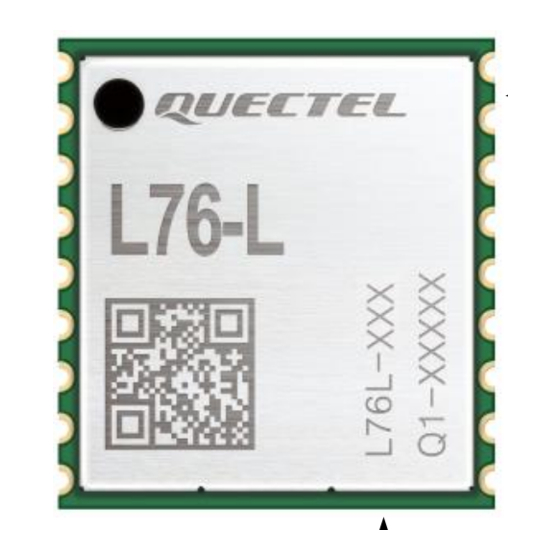
Page 56: Labelling Information
GNSS Module Series Labelling Information The label of the Quectel GNSS modules contains important product information. The location of the product type number is shown in figure below. Quectel Logo Pin1 indication Product Name Ordering Code Pin1 indication Quectel Logo... -
Page 57: Appendix References
Circular Error Probable CNR or C/N Carrier-to-noise Ratio Data Communications Equipment DCS1800 Digital Cellular System at 1800 MHz Dead Reckoning Data Terminal Equipment EASY Embedded Assist System EGNOS European Geostationary Navigation Overlay Service Extended Prediction Orbit Electrostatic Discharge L76&L76-L_Hardware_Design 56 / 59... - Page 58 Long-term Orbit Mbps Megabits per second Microcontroller Unit/Microprogrammed Control Unit MEMS Micro-Electro-Mechanical System Minimum Order Quantity Mass Production MSAS Multi-functional Satellite Augmentation System (Japan) Moisture Sensitivity Levels N. W Net Weight NMEA National Marine Electronics Association L76&L76-L_Hardware_Design 57 / 59...
- Page 59 GNSS Module Series Open Connector Printed Circuit Board Power Management Unit parts per million 1PPS One Pulse Per Second Quectel Proprietary Protocol PSRR Power Supply Rejection Ratio QR (code) Quick Response (Code) QZSS Quasi-Zenith Satellite System Random Access Memory Radio Frequency...
- Page 60 Static Random Access Memory TCXO Temperature Compensated Crystal Oscillator TTFF Time to First Fix Transient Voltage Suppressor UART Universal Asynchronous Receiver/Transmitter Coordinated Universal Time VSWR Voltage Standing Wave Ratio WAAS Wide Area Augmentation System XTAL External Crystal Oscillator L76&L76-L_Hardware_Design 59 / 59...
Need help?
Do you have a question about the L76 and is the answer not in the manual?
Questions and answers