
Related Manuals for Quectel AF31G


Summary of Contents for Quectel AF31G
- Page 1 AF31G Hardware Design Wi-Fi&Bluetooth Module Series Version: 1.0.1 Date: 2022-07-19 Status: Preliminary...
- Page 2 Wi-Fi&Bluetooth Module Series At Quectel, our aim is to provide timely and comprehensive services to our customers. If you require any assistance, please contact our headquarters: Quectel Wireless Solutions Co., Ltd. Building 5, Shanghai Business Park Phase III (Area B), No.1016 Tianlin Road, Minhang District, Shanghai...
- Page 3 Except as otherwise set forth herein, nothing in this document shall be construed as conferring any rights to use any trademark, trade name or name, abbreviation, or counterfeit product thereof owned by Quectel or any third party in advertising, publicity, or other aspects.
-
Page 4: Safety Information
Manufacturers of the cellular terminal should notify users and operating personnel of the following safety information by incorporating these guidelines into all manuals of the product. Otherwise, Quectel assumes no liability for customers’ failure to comply with these precautions. - Page 5 Wi-Fi&Bluetooth Module Series metal powders. AF31G_Hardware_Design 53 / 53...
-
Page 6: About The Document
Preliminary: 1. Updated the pin names: 20, 21, 24, 25, 27, 28, 58, 59, 60, 61, 62, 2. Updated the Pin Assignment (Figure 2) 3. Updated the weight of AF31G 1.0.1 2022-07-19 Barret XIONG (Table 2) 4. Updated the SDIO routing requirements (Chapter 4.1.1.2) -
Page 7: Table Of Contents
Wi-Fi&Bluetooth Module Series Contents Safety Information ............................3 About the Document ............................5 Contents ................................ 6 Table Index ..............................8 Figure Index ..............................9 1 Introduction .............................10 1.1. Special Mark ..........................10 2 Product Overview ........................... 11 2.1. Key Features ..........................12 2.2. Functional Diagram ........................13 2.3. - Page 8 Wi-Fi&Bluetooth Module Series 5.4. Antenna Requirements ........................34 5.5. RF Connector Recommendation ....................35 6 Electrical Characteristics & ........................37 7 Reliability ..............................38 7.1. Absolute Maximum Ratings ......................38 7.2. Digital I/O Characteristic ........................38 7.3. Power Consumption ........................39 7.3.1. Wi-Fi Power Consumption ....................39 7.3.2.
- Page 9 Table 14: Pin Definition of WLAN_SLP_CLK ....................28 Table 15: Pin Definition of RF Antenna Interface ..................29 Table 16: Operating Frequency of AF31G (Unit: GHz) ................29 Table 17: Conducted RF Output Power at 2.4 GHz (Unit: dBm) ..............30 Table 18: Conducted RF Output Power at 5 GHz (Unit: dBm) ..............31...
- Page 10 Wi-Fi&Bluetooth Module Series Figure Index Figure 1: Functional Diagram ........................13 Figure 2: Pin Assignment (Top View) ......................14 Figure 3: Reference Circuit for VDD_PA .....................20 Figure 4: Reference Circuit for VDD_IO ......................20 Figure 5: Power-up Timing .......................... 21 Figure 6: Wi-Fi Application Interface Connection ..................22 Figure 7: PCIe Interface Connection ......................
-
Page 11: Introduction
Wi-Fi&Bluetooth Module Series Introduction This document, describing AF31G and its air interface and hardware interfaces connected to your applications, informs you of the interface and RF specifications, electrical and mechanical details, as well as other related information of the module. -
Page 12: Product Overview
Wi-Fi&Bluetooth Module Series Product Overview AF31G is an automotive grade Wi-Fi and Bluetooth module with low power consumption. It is complying with IEEE 802.11a/b/g/n/ac 2.4 GHz & 5 GHz WLAN standards and Bluetooth 5.0 standard, which enables seamless integration of WLAN and Bluetooth Low Energy technologies. -
Page 13: Key Features
Wi-Fi&Bluetooth Module Series 2.1. Key Features Table 3: Key Features Parameter Details VDD_PA: 3.14–3.46 V Typical: 3.3 V Power Supply VDD_IO: 1.71–1.89 V Typical: 1.8 V Wi-Fi: 2.4 GHz: 2.400–2.4835 GHz Frequency Range 5 GHz: 5.150–5.850 GHz ... -
Page 14: Functional Diagram
Wi-Fi&Bluetooth Module Series Operating Temperature Range: -40 °C to +85 °C Operating Temperature Storage temperature range: -40 °C to +95 °C RoHS All hardware components are fully compliant with EU RoHS directive. 2.2. Functional Diagram The following figure shows a block diagram of the module and illustrates the major functional parts. Power management ... -
Page 15: Pin Assignment
Wi-Fi&Bluetooth Module Series 2.3. Pin Assignment Figure 2: Pin Assignment (Top View) NOTE Please keep all RESERVED pins open. SDIO interface and PCIe interface exist in different hardware modules respectively. Modules supporting PCIe interface do not support SDIO interface. At this time, it is necessary to suspend the pins of all SDIO interfaces, and vice versa. -
Page 16: Pin Description
Wi-Fi&Bluetooth Module Series 2.4. Pin Description Table 4: Parameters Definition Parameter Description Analog input Analog output Digital Input Digital output Open drain Power input Power output Table 5: Pin Description Power Supply Pin Name Pin No. Description Comments Characteristics It must be Main Power 101, 102, provided with... - Page 17 Wi-Fi&Bluetooth Module Series VDD_IO power Bluetooth BT_EN domain. enable control Active high. PCM_DIN PCM data input PCM data PCM_SYNC frame sync PCM_CLK PCM clock PCM data PCM_DOUT output VDD_IO power Bluetooth domain. BT_TXD UART transmit Bluetooth BT_RXD UART receive Request To BT_RTS Send BT_CTS...
- Page 18 Wi-Fi&Bluetooth Module Series clock (+) differential impedance of 85 PCIe reference Ω. PCIE_CLK_M clock (-) PCIe transmit PCIE_TX_P PCIe transmit PCIE_TX_M PCIe receive PCIE_RX_P PCIE_RX_M PCIe receive (-) PCIe clock PCIE_CLKREQ_N request VDD_IO power PCIe wakes up 1.8 V PCIE_WAKE_N domain.
- Page 19 Wi-Fi&Bluetooth Module Series interface 2.4/5 GHz Wi-Fi ANT_WIFI1 antenna interface 1 Reserved Interface Pin Name Pin No. Comments 10, 31, 32, 33, 34, 37, 41, 42, 48, 49, 50, 51, 57, 58, 59, 60, 61, 62, 63, 64, 65, RESERVED 66, 77, 79, 83, 85, 86, 89 AF31G_Hardware_Design 53 / 53...
-
Page 20: Operating Characteristics
3.1.2. Reference Design for Power Supply AF31G is powered by VDD_PA, and it is recommended to use a power supply chip with maximum output current exceeding 1.5 A. The following figure shows a reference design for VDD_PA is controlled by WLAN_PWR_EN1. - Page 21 Figure 3: Reference Circuit for VDD_PA The power supply for I/O in AF31G is from VDD_IO, and it is recommended to use a power supply chip with maximum output current exceeding 300 mA. The following figure shows a reference design for VDD_IO is controlled by WLAN_PWR_EN2.
-
Page 22: Timing Of Turning On The Module
Wi-Fi&Bluetooth Module Series 3.1.3. Timing of Turning on the Module Figure 5: Power-up Timing AF31G_Hardware_Design 53 / 53... -
Page 23: Application Interfaces
Wi-Fi&Bluetooth Module Series Application Interfaces 4.1. Wireless Connection Interface AF31G supports low power PCIe Gen2 interface or SDIO 3.0 for Wi-Fi function and UART as well as PCM interfaces for Bluetooth function. 4.1.1. Wi-Fi Application Interface The following figure shows the Wi-Fi application interface connection between AF31G and AG52x series modules. - Page 24 PCIE_RST_N PCIe reset The following figure shows the PCIe interface connection between AF31G and AG52x series modules. Figure 7: PCIe Interface Connection In order to ensure the integrity of PCIe signal, C1 and C2 components must be placed close to AG52x series modules.
-
Page 25: Sdio Interface
WLAN SDIO data bus D1 WLAN_SDIO_DATA2 WLAN SDIO data bus D2 WLAN_SDIO_DATA3 WLAN SDIO data bus D3 The following figure shows the SDIO interface connection between AF31G and AG52x series modules. Figure 8: SDIO Interface Connection AF31G_Hardware_Design 53 / 53... -
Page 26: Wlan_En
Make sure the adjacent trace spacing is 2 times of the trace width and bus capacitance is less than 15 pF. 4.1.1.3. WLAN_EN WLAN_EN is used to control the Wi-Fi function of AF31G. Wi-Fi function will be enabled when WLAN_EN is at high level. Table 9: Pin Definition of WLAN_EN Pin Name Pin No. -
Page 27: Bluetooth Application Interface
PCM data frame sync VDD_IO power domain. PCM_CLK PCM clock PCM_DOUT PCM data output The following figure shows the PCM interface connection between AF31G and AG52x series modules. Figure 10: Block Diagram of PCM Interface Connection AF31G_Hardware_Design 53 / 53... -
Page 28: Bt_En
Wi-Fi&Bluetooth Module Series 4.1.2.2. BT_EN BT_EN is used to control the Bluetooth function of AF31G. Bluetooth function will be enabled when BT_EN is at high level. Table 11: Pin Definition of BT_EN Pin Name Pin No. Description Comments VDD_IO power domain. -
Page 29: Coexistence Uart
COEX_RXD receive The following figure shows the reference design for coexistence UART interface connection between AF31G and AG52x series modules. Figure 12: Coexistence UART Interface Connection 4.3. WLAN_SLP_CLK The 32.768 kHz clock can be used in low power consumption mode, such as power saving mode and sleep mode, in which basic logic operations can be maintained. -
Page 30: Rf Specifications
2.402–2.480 5.1.2. Reference Design AF31G provides an RF antenna pin for Wi-Fi/Bluetooth antenna connection. The RF trace in host PCB connected to the module’s RF antenna pin should be microstrip line or other types of RF trace, with characteristic impendence close to 50 Ω. This module comes with grounding pins which are next to the antenna pin in order to give a better grounding. -
Page 31: Rf Performances
Wi-Fi&Bluetooth Module Series TVS (D1) should be placed as close to the antenna as possible. The capacitors and inductors are not mounted by default. The parasitic capacitance of TVS should be less than 0.05 pF. Figure 13: Reference Design for RF Antenna Interface 5.2. - Page 32 Wi-Fi&Bluetooth Module Series Table 18: Conducted RF Output Power at 5 GHz (Unit: dBm) Standard Data Rate Typ. 802.11a 6 Mbps 802.11a 54 Mbps 802.11n, HT20 MCS 0 802.11n, HT20 MCS 7 802.11n, HT40 MCS 0 802.11n, HT40 MCS 7 802.11ac, VHT20 MCS 0 802.11ac, VHT20...
-
Page 33: Conducted Rf Performance Of Ble
Wi-Fi&Bluetooth Module Series Table 20: Conducted RF Receiving Sensitivity at 5 GHz (Unit: dBm) Standard Data Rate Typ. 802.11a 6 Mbps 802.11a 54 Mbps 802.11n, HT20 MCS 0 802.11n, HT20 MCS 7 802.11n, HT40 MCS 0 802.11n, HT40 MCS 7 802.11ac, VHT20 MCS 0 802.11ac, VHT20... -
Page 34: Reference Design Of Rf Routing
Wi-Fi&Bluetooth Module Series 5.3. Reference Design of RF Routing For user’s PCB, the characteristic impedance of all RF traces should be controlled to 50 Ω. The impedance of the RF traces is usually determined by the trace width (W), the materials’ dielectric constant, the height from the reference ground to the signal layer (H), and the spacing between RF traces and grounds (S). -
Page 35: Antenna Requirements
Wi-Fi&Bluetooth Module Series Figure 17: Coplanar Waveguide Design on a 4-layer PCB (Layer 4 as Reference Ground) In order to ensure RF performance and reliability, follow the principles below in RF layout design: Use an impedance simulation tool to accurately control the characteristic impedance of RF traces to ... -
Page 36: Rf Connector Recommendation
Wi-Fi&Bluetooth Module Series Polarization Type Vertical 5.5. RF Connector Recommendation If the RF connector is used for antenna connection, it is recommended to use U.FL-R-SMT connectors provided by Hirose. Figure 18: Dimensions of the Receptacle (Unit: mm) U.FL-LP series connectors listed in the following figure can be used to match the U.FL-R-SMT. Figure 19: Specifications of Mated Plugs (Unit: mm) The following figure describes the space factor of the mated connector. - Page 37 Wi-Fi&Bluetooth Module Series Figure 20: Space Factor of the Mated Connectors (Unit: mm) For more details, visit http://www.hirose.com. AF31G_Hardware_Design 53 / 53...
-
Page 38: Electrical Characteristics
Wi-Fi&Bluetooth Module Series Electrical Characteristics & AF31G_Hardware_Design 53 / 53... -
Page 39: Reliability
+ 0.2 DDIO NOTE is the supply voltage associated with the input pin to which the test voltage is applied. DDIO The following table shows the recommended operating conditions of AF31G. Table 24: Recommended Operating Conditions (Unit: V) Parameter Min. Typ. -
Page 40: Power Consumption
Wi-Fi&Bluetooth Module Series Table 25: General DC Electrical Characteristics Parameter Description Min. Max. Unit High Level Input Voltage 0.7 × VDD_IO VDD_IO + 0.2 Low Level Input Voltage -0.3 0.3 × VDD_IO High Level Output Voltage 0.9 × VDD_IO VDD_IO Low Level Output Voltage 0.3 ×... -
Page 41: Ble Power Consumption
Table 27: BLE Power Consumption During Non-signaling Description Power Power Supply Consumed Current 3.3 V Non-signaling TBD dBm 1.8 V NOTE For more details about current consumption, please contact Quectel Technical Supports for the power consumption test report of the module. AF31G_Hardware_Design 53 / 53... -
Page 42: Esd Protection
Wi-Fi&Bluetooth Module Series 7.4. ESD Protection Static electricity occurs naturally and it may damage the module. Therefore, applying proper ESD countermeasures and handling methods is imperative. For example, wear anti-static gloves during the development, production, assembly and testing of the module; add ESD protection components to the ESD sensitive interfaces and points in the product design. -
Page 43: Operating And Storage Temperatures
Wi-Fi&Bluetooth Module Series Fasten the heatsink with four screws to ensure that it is in close contact with the module to prevent the heatsink from falling off during the drop, vibration test, or transportation. Figure 21: Placement and Fixing of the Heatsink 7.6. -
Page 44: Mechanical Information
Wi-Fi&Bluetooth Module Series Mechanical Information This chapter describes the mechanical dimensions of the module. All dimensions are measured in millimeter (mm), All dimensions are measured in millimeter (mm), and the dimensional tolerances are ±0.2 mm unless otherwise specified. 8.1. Mechanical Dimensions Figure 22: Module Top and Side Dimensions AF31G_Hardware_Design 53 / 53... - Page 45 Wi-Fi&Bluetooth Module Series Figure 23: Module Bottom Dimension (Bottom View) NOTE The package warpage level of the module conforms to the JEITA ED-7306 standard. AF31G_Hardware_Design 53 / 53...
-
Page 46: Recommended Footprint
Wi-Fi&Bluetooth Module Series 8.2. Recommended Footprint Figure 24: Recommended Footprint NOTE Keep at least 3 mm between the module and other components on the motherboard to improve soldering quality and maintenance convenience. AF31G_Hardware_Design 53 / 53... -
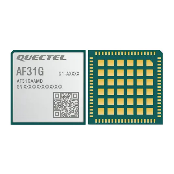
Page 47: Top And Bottom Views
8.3. Top and Bottom Views Figure 25: Top View of the Module NOTE Images above are for illustration purpose only and may differ from the actual module. For authentic appearance and label, please refer to the module received from Quectel. AF31G_Hardware_Design 53 / 53... -
Page 48: Storage, Manufacturing And Packaging
Wi-Fi&Bluetooth Module Series Storage, Manufacturing and Packaging 9.1. Storage Conditions The module is provided with vacuum-sealed packaging. MSL of the module is rated as 3. The storage requirements are shown below. 1. Recommended Storage Condition: the temperature should be 23 ±5 °C and the relative humidity should be 35–60 %. -
Page 49: Manufacturing And Soldering
Wi-Fi&Bluetooth Module Series NOTE 1. To avoid blistering, layer separation and other soldering issues, extended exposure of the module to the air is forbidden. 2. Take out the module from the package and put it on high-temperature-resistant fixtures before baking. -
Page 50: Packaging Specifications
Avoid using ultrasonic technology for module cleaning since it can damage crystals inside the module. Due to the complexity of the SMT process, please contact Quectel Technical Supports in advance for any situation that you are not sure about, or any process (e.g. selective soldering, ultrasonic soldering) that is not mentioned in document [1][2]. -
Page 51: Carrier Tape
Wi-Fi&Bluetooth Module Series 9.3.1. Carrier Tape Dimension details are as follow: Figure 22: Carrier Tape Dimension Drawing Table 31: Carrier Tape Dimension Table (Unit: mm) 23.5 23.5 20.2 1.75 9.3.2. Plastic Reel Figure 23: Plastic Reel Dimension Drawing AF31G_Hardware_Design 53 / 53... -
Page 52: Packaging Process
Wi-Fi&Bluetooth Module Series Table 32: Plastic Reel Dimension Table (Unit: mm) øD1 øD2 44.5 9.3.3. Packaging Process Place the module into the carrier tape and use the cover tape to cover it; then wind the heat-sealed carrier tape to the plastic reel and use the protective tape for protection. - Page 53 Wi-Fi&Bluetooth Module Series Put 4 packaged pizza boxes into 1 cartoon box and seal it. 1 cartoon box can pack 1000 modules. Figure 24: Packaging Process AF31G_Hardware_Design 53 / 53...
-
Page 54: Appendix References
Wi-Fi&Bluetooth Module Series Appendix References Table 33: Related Documents Document Name [1] Quectel_Module_Secondary_SMT_Application_Note [2] Quectel_RF_Layout_Application_Note Table 34: Terms and Abbreviations Abbreviation Description Bytes per second CDMA Code Division Multiple Access CHAP Challenge Handshake Authentication Protocol Coding Scheme Clear To Send Electrostatic Discharge Ground HSIC... - Page 55 Wi-Fi&Bluetooth Module Series Phase Shift Keying Quadrature Amplitude Modulation QPSK Quadrature Phase Shift Keying Radio Frequency RoHS Restriction of Hazardous Substances Request To Send Short Message Service UART Universal Asynchronous Receiver/Transmitter Vmax Maximum Voltage Vnom Nominal Voltage Vmin Minimum Voltage Maximum High-level Input Voltage Minimum High-level Input Voltage Maximum Low-level Input Voltage...
- Page 56 FCC Certification Requirements. According to the definition of mobile and fixed device is described in Part 2.1091(b), this device is a mobile device. And the following conditions must be met: 1. This Modular Approval is limited to OEM installation for mobile and fixed applications only.
- Page 57 For portable devices, in addition to the conditions 3 through 6 described above, a separate approval is required to satisfy the SAR requirements of FCC Part 2.1093 If the device is used for other equipment that separate approval is required for all other operating configurations, including portable configurations with respect to 2.1093 and different antenna configurations.
- Page 58 responsible for compliance could void the user's authority to operate the equipment. In cases where the manual is provided only in a form other than paper, such as on a computer disk or over the Internet, the information required by this section may be included in the manual in that alternative form, provided the user can reasonably be expected to have the capability to access information in that form.
Need help?
Do you have a question about the AF31G and is the answer not in the manual?
Questions and answers