
Related Manuals for Quectel EG915Q-NA


Summary of Contents for Quectel EG915Q-NA
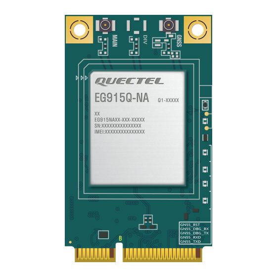
- Page 1 EG915Q-NA&EG916Q-GL Hardware Design LTE Standard Module Series Version: 1.1 Date: 2023-10-19 Status: Released...
-
Page 2: Legal Notices
LTE Standard Module Series At Quectel, our aim is to provide timely and comprehensive services to our customers. If you require any assistance, please contact our headquarters: Quectel Wireless Solutions Co., Ltd. Building 5, Shanghai Business Park Phase III (Area B), No.1016 Tianlin Road, Minhang District, Shanghai... -
Page 3: Third-Party Rights
Except as otherwise set forth herein, nothing in this document shall be construed as conferring any rights to use any trademark, trade name or name, abbreviation, or counterfeit product thereof owned by Quectel or any third party in advertising, publicity, or other aspects. -
Page 4: Safety Information
Manufacturers of the terminal should notify users and operating personnel of the following safety information by incorporating these guidelines into all manuals of the product. Otherwise, Quectel assumes no liability for customers’ failure to comply with these precautions. -
Page 5: About The Document
LTE Standard Module Series About the Document Revision History Version Date Author Description Lex LI/ 2022-11-28 Creation of the document Lena HUANG Lex LI/ 2023-02-06 First official release Barry DENG Added an applicable module EG916Q-GL. Updated the following pins: pin 25: from SPI_CS to RESERVED. pin 26: from SPI_CLK to RESERVED. - Page 6 LTE Standard Module Series Added operating modes GNSS part (Chapter 3.1.2). Added the summary of LTE and GNSS Parts’ State in All-in-one solution (Chapter 3.1.3). 10. Added the summary of LTE and GNSS Parts’ State in stand-alone solution (Chapter 3.1.4). 11.
-
Page 7: Table Of Contents
LTE Standard Module Series Contents Safety Information ............................3 About the Document ..........................4 Contents ..............................6 Table Index ..............................9 Figure Index .............................. 11 1 Introduction ............................13 1.1. Special Marks ..........................13 2 Product Overview ..........................14 2.1. Frequency Bands and Functions ....................14 2.2. - Page 8 LTE Standard Module Series 4.2. USB_BOOT..........................40 4.3. USIM Interfaces ........................... 42 4.4. UART Interfaces ........................... 44 4.5. PCM and I2C Interfaces* ......................47 4.6. ADC Interfaces ..........................48 4.7. Camera SPI Interface* ......................... 49 4.8. GRFC Interfaces .......................... 49 4.9.
- Page 9 LTE Standard Module Series 9.3.1. Carrier Tape ........................81 9.3.2. Plastic Reel ........................82 9.3.3. Mounting Direction ......................82 9.3.4. Packaging Process ......................83 10 Appendix References ........................84 EG15Q-NA&EG916Q-GL_Hardware_Design 8 / 93...
- Page 10 Table 38 : Absolute Maximum Ratings ....................... 65 Table 39 : Power Supply Ratings ....................... 65 Table 40 : Power Consumption of EG915Q-NA LTE Part (GNSS Part Off) ..........66 Table 41 : Power Consumption of EG916Q-GL LTE Part (GNSS Part Off)..........66 EG15Q-NA&EG916Q-GL_Hardware_Design...
- Page 11 LTE Standard Module Series Table 42 : VDD_EXT I/O Characteristics (Unit: V) ..................68 Table 43 : USIM Low-voltage I/O Characteristics (Unit: V) ................ 68 Table 44 : USIM High-voltage I/O Characteristics (Unit: V) ............... 68 Table 45 : ESD Characteristics (Temperature: 25–30 ° C, Humidity: 40 ± 5 %; Unit: kV) ......69 Table 46 : Operating and Storage Temperatures (Unit: °...
- Page 12 Figure 38 : Specifications of Mated Plugs ....................63 Figure 39 : Space Factor of Mated Connectors (Unit: mm) ............... 64 Figure 40 : EG915Q-NA Top and Side Dimensions (Unit: mm) ..............71 Figure 41 : EG916Q-GL Top and Side Dimensions (Unit: mm) ..............72 Figure 42 : EG915Q-NA Bottom Dimensions (Bottom View, Unit: mm) ............
- Page 13 Figure 44 : EG915Q-NA Recommended Footprint (Unit: mm) ..............75 Figure 45 : EG916Q-GL Recommended Footprint (Unit: mm) ..............76 Figure 46 : EG915Q-NA Top and Bottom Views of the Module ..............77 Figure 47 : EG916Q-GL Top and Bottom Views of the Module ..............77 Figure 48 : Recommended Reflow Soldering Thermal Profile ..............
-
Page 14: Introduction
LTE Standard Module Series Introduction This document describes the EG915Q-NA and EG916Q-GL features, performance, and air interfaces and hardware interfaces connected to your applications. The document provides a quick insight into interface specifications, RF performance, electrical and mechanical specifications, and other module information, as well. -
Page 15: Product Overview
LTE Standard Module Series Product Overview EG915Q-NA and EG916Q-GL are SMD modules with compact packaging, which also support GNSS to meet your specific application demands. Table 2: Basic Information Item EG915Q-NA EG916Q-GL Packaging type Pin counts (23.6 ± 0.2) mm × (19.9 ± 0.2) mm ×... -
Page 16: Key Features
LTE Standard Module Series 2.2. Key Features Table 4: Key Features Categories Descriptions ⚫ 3.3–4.3 V Supply Voltage ⚫ Typ.: 3.8 V ⚫ Text and PDU mode ⚫ Point-to-point MO and MT ⚫ SMS cell broadcast ⚫ SMS storage: ME by default ⚫... - Page 17 RoHS All hardware components fully comply with EU RoHS directive NOTE EG915Q-NA and EG916Q-GL support SPI interface. If you need this function, please contact Quectel Technical Support. Within the operating temperature range, the module meets 3GPP specifications. Within the extended temperature range, the module remains the ability to establish and maintain functions such as SMS and data transmission, without any unrecoverable malfunction.
-
Page 18: Pin Assignment
RESERVED RESERVED RESET_ N VBAT_ BB W_DISABLE# VBAT_ BB USB Pins Signal Pins Power Pins I2C Pins GND Pins RESERVED Pins UART Pins PCM Pins (U)SIM Pins ADC Pins Figure 1: EG915Q-NA Pin Assignment (Top View) EG15Q-NA&EG916Q-GL_Hardware_Design 17 / 93... - Page 19 LTE Standard Module Series PS M_IND ANT_GNSS ADC1 GNSS_RST RESE RV ED RESE RV ED RESE RV ED PCM_CLK USIM1_CLK RESE RV ED RESE RV ED RESE RV ED CA M_PWD N G NSS _VBC KP PCM_SY NC USIM1_DATA RESE RV ED PCM_DIN RESE RV ED USIM1_RST...
-
Page 20: Pin Description
LTE Standard Module Series be 1.8 V. Otherwise, USIM2 interface will be damaged. 4. The module supports SPI interface. If you need this function, please contact Quectel Technical Support. 5. GNSS interface (Pins 27, 28, 49, 51, 109, 110, 112, 117, 118) is optional. If you need this function, please contact Quectel Technical Support. - Page 21 Pin No. Description Comment Characteristic Vmax = 5.25 V A test point must be USB_VBUS USB connection detect Vmin = 3.0 V reserved. This pin is optional. If you need this function, please contact Quectel Technical Support. EG15Q-NA&EG916Q-GL_Hardware_Design 20 / 93...
- Page 22 LTE Standard Module Series Vnom = 5.0 V USB 2.0 compliant. USB_DP USB differential data (+) Requires differential impedance of 90 Ω. Test points must be USB_DM USB differential data (-) reserved. USIM Interfaces Pin Name Pin No. Description Comment Characteristic max = 50 mA Either 1.8 V or 3.0 V...
- Page 23 LTE Standard Module Series damaged. Connected with pin 78 (CAM_SPI_ CLK) internally. 1.8 V power domain USIM2_RST USIM2 card reset is required for USIM2. Otherwise, this interface will be damaged. Connected with pin 115 (CAM_ PWDN) internally. 1.8 V power domain USIM2_CLK USIM2 card clock is required for...
- Page 24 LTE Standard Module Series DBG_RXD Debug UART receive Test points must be VDD_EXT reserved. DBG_TXD Debug UART transmit GNSS UART Pin Name Pin No. Description Comment Characteristic GNSS_TXD GNSS UART transmit If unused, keep them VDD_EXT open. GNSS_RXD GNSS UART receive GNSS debug UART Pin Name Pin No.
- Page 25 LTE Standard Module Series 50 Ω impedance. ANT_GNSS GNSS antenna interface GRFC Interfaces Pin Name Pin No. Description Comment Characteristic GRFC1 Generic RF controller If unused, keep them VDD_EXT open. GRFC2 Generic RF controller Camera SPI Interface* Pin Name Pin No. Description Comment Characteristic...
-
Page 26: Evb Kit
111, 113, 114, 116, 119–126 open. 2.5. EVB Kit To help you develop applications with the module, Quectel supplies an evaluation board (UMTS<E EVB) with accessories to develop or test the module. For more details, see document [1]. EG15Q-NA&EG916Q-GL_Hardware_Design 25 / 93... -
Page 27: Operating Characteristics
LTE Standard Module Series Operating Characteristics 3.1. Operating Modes The module integrates both LTE and GNSS engines which can work as a whole (All-in-one solution) unit or work independently (Stand-alone solution) according to your demands. 3.1.1. Operating Modes of LTE Part Table 7: Operating Modes Overview of LTE Part Modes Descriptions... -
Page 28: Sleep Mode
LTE Standard Module Series 3.1.1.1. Sleep Mode With DRX technology, power consumption of the module will be reduced to an ultra-low level. DRX OFF ON Run time Figure 3: Power Consumption During Sleep Mode NOTE The DRX cycle values are transmitted sent over the wireless network. 3.1.1.2. -
Page 29: Usb Application With Usb Remote Wakeup Function
LTE Standard Module Series ⚫ Driving MAIN_DTR low with the MCU will wake up the module. ⚫ When the module has a URC to report, MAIN_RI signal will wake up the MCU. See Chapter 4.10.3 for details about MAIN_RI. 3.1.1.3. USB Application with USB Remote Wakeup Function* If the host supports USB suspend/resume and remote wakeup functions, the following three preconditions must be met to set the module to sleep mode. -
Page 30: Usb Application Without Usb Suspend Function
LTE Standard Module Series Module Host USB_VBUS USB_DP USB_DP USB_DM USB_DM GPIO AP_READY EINT MAIN_RI Figure 6: Sleep Mode Application with USB Suspend/Resume and MAIN_RI ⚫ Sending data to the module through USB will wake up the module. ⚫ When the module has a URC to report, the module will wake up the host through MAIN_RI signal. See Chapter 4.10.3 for details about MAIN_RI behavior. -
Page 31: Airplane Mode
LTE Standard Module Series NOTE Pay attention to the level match shown in the dotted line between the module and the host. 3.1.1.6. Airplane Mode When the module enters airplane mode, the RF function will be disabled, and all AT commands correlative with RF function will be inaccessible. -
Page 32: Summary Of Lte And Gnss Parts' State In All-In-One Solution
LTE Standard Module Series ⚫ Power Down The power supply inside and outside the GNSS is cut off. ⚫ Mode The software stops working. 3.1.3. Summary of LTE and GNSS Parts’ State in All-in-one Solution In All-in-one solution, LTE part and GNSS part can be worked as a whole unit. The GNSS part can be regarded as a peripheral of the LTE part. -
Page 33: Power Supply
LTE Standard Module Series DC_IN VBAT GNSS UART Switch PWRKEY GNSS_VSYS GNSS_PWR_EN GNSS debug UART GNSS GNSS_VRTC (Test points must be GNSS_VBCKP reserved.) Module LDO_EN rechargeable GNSS_RST GNSS_PPS Main UART battery is optional Figure 9: Stand-alone Solution Schematic Diagram 3.2. Power Supply 3.2.1. -
Page 34: Voltage Stability Requirements
LTE Standard Module Series DC_IN VBAT 100K 330R 4.7K 470 µF 100 nF 470 µF 100 nF VBAT_EN Figure 10: Reference Design of Power Input ⚫ NOTE To avoid corrupting the data in the internal flash, do not switch off the power supply when the module works normally. -
Page 35: Turn On
LTE Standard Module Series VBAT VBAT _RF VBAT _BB 100 nF 10 pF 100 µF 33 pF 100 µF 100 nF 33 pF 10 pF Module Figure 11: Reference Design of Power Supply Turn On 3.3. 3.3.1. Turn On with PWRKEY Table 10: Pin Description of PWRKEY Pin Name Pin No. - Page 36 LTE Standard Module Series Another way to control the PWRKEY is using a keystroke directly. When pressing the keystroke, an electrostatic strike may be generated from finger. Therefore, you should place a TVS component near the keystroke for ESD protection. PWRKEY 500 ms Module...
-
Page 37: Turn Off
LTE Standard Module Series NOTE 1. Ensure the voltage of VBAT is stable for at least 30 ms before driving the PWRKEY low. 2. If the module needs to turn on automatically but does not need the turn-off function, PWRKEY can be driven low directly to ground with a recommended 4.7 kΩ... -
Page 38: Reset
LTE Standard Module Series of the command. Otherwise, the module will be turned on automatically again after successful turn-off. 3.5. Reset The reset function requires the PWRKEY and RESET_N pins to work together to complete. Pulling down PWRKEY when RESET_N is at low level can reset the module. The RESET_N signal is sensitive to interference, so it is recommended to route the trace as short as possible and surround it with ground. - Page 39 LTE Standard Module Series 500 ms PWRKEY Turn on pulse 4.7K GPIO Module Figure 17: Reference Design of PWRKEY with Driving Circuit VBAT ≥ 500 ms PWRKEY ≤ 0.5 V ≥ 300 ms RESET_N ≤ 0.5 V Module Running Resetting Restart Status Figure 18: Reset Timing...
-
Page 40: Application Interfaces
LTE Standard Module Series Application Interfaces 4.1. USB Interface The module provides one integrated Universal Serial Bus (USB) interface which complies with the USB 2.0 specifications and supports high-speed (480 Mbps) and full-speed (12 Mbps) for USB 2.0. The module only supports USB slave mode. The USB interface can be used for AT command communication, data transmission, GNSS NMEA sentence output (All-in-one mode only), software debugging, firmware upgrade and the output of partial logs. -
Page 41: Usb_Boot
LTE Standard Module Series It is recommended to add a common-mode choke L1 in series between MCU and the module to suppress EMI spurious transmission. Meanwhile, it is also suggested to add R1 and R2 in series between the module and test points for debugging. These resistors are not mounted by default. To ensure the signal integrity of USB 2.0 data transmission, you should place L1, R1 and R2 close to the module, and keep these resistors close to each other. - Page 42 LTE Standard Module Series Test points 4.7K TVS should be placed close to test points. Figure 20: Reference Design of USB_BOOT NOTE 1 VBAT 500 ms PWRKEY 0.5 V About 40 ms VDD_EXT USB_BOOT RESET_N Figure 21: Timing of Entering Emergency Download Mode NOTE 1.
-
Page 43: Usim Interfaces
LTE Standard Module Series 4.3. USIM Interfaces The USIM interfaces meets ETSI and IMT-2000 requirements. ⚫ USIM1 interface supports 1.8 V or 3.0 V power domain. ⚫ USIM2 interface only supports 1.8 V power domain. ⚫ When USIM1 and USIM2 are used at the same time, the power domain of USIM interfaces should be 1.8 V. - Page 44 LTE Standard Module Series USIM2. Otherwise, this interface will be damaged. The module supports USIM1 card hot-plug via the USIM1_DET, and both high-level and low-level detections are supported. Hot-plug function is disabled by default and you can use AT+QSIMDET to configure this function.
-
Page 45: Uart Interfaces
LTE Standard Module Series When only USIM1 interface is used, please make sure USIM2_VDD that these two 10K resistors are not soldered. 100 nF USIM Card Connector USIM2_VDD USIM2_RST Module USIM2_CLK USIM2_DATA 33 pF 33 pF 33 pF TVS Array Figure 24: Reference Design of USIM2 Interface with a 6-pin USIM Card Connector To enhance the reliability and availability of the USIM cards in applications, follow the principles below in the USIM circuit design:... - Page 46 If unused, keep them open. GNSS_RXD GNSS UART receive GNSS_DBG_TXD GNSS debug UART transmit Test points must be reserved. GNSS_DBG_RXD GNSS debug UART receive This pin is optional. If you need this function, please contact Quectel Technical Support. EG15Q-NA&EG916Q-GL_Hardware_Design 45 / 93...
- Page 47 LTE Standard Module Series The module provides 1.8 V UART interfaces. You can use a level-shifting chip between the module and host’s UART if the host is equipped with a 3.3 V UART. VDD_EXT VCCA VCCB VDD_MCU 0.1 μ F 0.1 μ...
-
Page 48: Pcm And I2C Interfaces
LTE Standard Module Series 4.5. PCM and I2C Interfaces* The module provides one Pulse Code Modulation (PCM) digital interface and one I2C interface. Table 17: Pin Description of PCM and I2C Interfaces Pin Name Pin No. Description Comment PCM_SYNC PCM data frame sync PCM_CLK PCM clock If unused, keep them open. -
Page 49: Adc Interfaces
LTE Standard Module Series 4.6. ADC Interfaces The module provides two Analog-to-Digital Converter (ADC) interfaces. To improve the accuracy of ADC, surround the trace of ADC with ground. Table 18: Pin Description of ADC Interfaces Pin Name Pin No. Description Comment ADC0 General-purpose ADC interface... -
Page 50: Camera Spi Interface
LTE Standard Module Series 4.7. Camera SPI Interface* The module provides one camera SPI interface supporting 2-bit data transmission of SPI. USIM2 and Camera SPI interface cannot be used at the same time. Table 20: Pin Description of Camera SPI Interface Pin Name Pin No. -
Page 51: Control Signals
Airplane mode AT+CFUN=4 NOTE W_DISABLE# is a control function for airplane mode, which is disabled in software by default. It can be enabled through AT+QCFG="airplanecontrol",1*. For the details of this command, please contact Quectel Technical Support. EG15Q-NA&EG916Q-GL_Hardware_Design 50 / 93... -
Page 52: Indication Signals
LTE Standard Module Series 4.10. Indication Signals Table 24: Pin Description of Indication Signals Pin Name Pin No. I/O Description Comment STATUS Indicate the module's operation status If unused, keep NET_STATUS 21 Indicate the module's network activity status them open. GNSS_PPS GNSS pulse per second output 4.10.1. -
Page 53: Status
LTE Standard Module Series 4.10.2. STATUS The STATUS is used for indicating the module’s operation status. It will output high level when the module is turned on. VBAT Module 2.2K 4.7K STATUS Figure 29: Reference Design of STATUS 4.10.3. MAIN_RI AT+QCFG= “risignaltype”, “physical”... -
Page 54: Rf Specifications
50 Ω impedance. ANT_MAIN Main antenna interface NOTE EG915Q-NA and EG916Q-GL support Wi-Fi scan function, and this function and LTE network cannot be used simultaneously since they share the same antenna interface. Table 28: Operating Frequency of EG915Q-NA (Unit: MHz) Operating Frequency... - Page 55 LTE Standard Module Series LTE-FDD B66 1710–1780 2110–2180 Table 29: Operating Frequency of EG916Q-GL (Unit: MHz) Operating Frequency Transmit Receive LTE-FDD B1 1920–1980 2110–2170 LTE-FDD B2 1850–1910 1930–1990 LTE-FDD B3 1710–1785 1805–1880 LTE-FDD B4 1710–1755 2110–2155 LTE-FDD B5 824–849 869–894 LTE-FDD B7 2500–2570 2620–2690...
-
Page 56: Tx Power
Max. RF Output Power Min. RF Output Power LTE bands 23 dBm ± 2 dB < -39 dBm 5.1.3. Rx Sensitivity Table 31: Conducted RF Receiver Sensitivity of EG915Q-NA (Unit: dBm) Receiver Sensitivity (Typ.) Frequency Bands 3GPP (SIMO) Primary LTE-FDD B2 (10 MHz) -98 dBm -94.3 dBm... -
Page 57: Reference Design
LTE Standard Module Series LTE-FDD B8 (10 MHz) -99.3 dBm -93.3 dBm LTE-FDD B12 (10 MHz) -99.5 dBm -93.3 dBm LTE-FDD B13 (10 MHz) -98.3 dBm -93.3 dBm LTE-FDD B18 (10 MHz) -99.3 dBm -96.3 dBm LTE-FDD B19 (10 MHz) -99.1 dBm -96.3 dBm LTE-FDD B20 (10 MHz) -
Page 58: Gnss (Optional)
LTE Standard Module Series NOTE Use a π-type matching circuit for the antenna interface for better cellular performance and for the ease of debugging. Capacitors are not mounted by default. π-type matching components (R1 & C1 & C2) to the antenna as close as possible. Place the 5.2. -
Page 59: Gnss Performance
LTE Standard Module Series 5.2.2. GNSS Performance Table 35: GNSS Performance of EG915Q-NA Parameter Description Conditions Typ. Unit Acquisition -145 Sensitivity Reacquisition Autonomous -157 Tracking -160 Autonomous 27.43 Cold start @ open sky AGPS enabled TTFF Warm start @ open sky Autonomous 27.37... -
Page 60: Reference Design
LTE Standard Module Series 5.2.3. Reference Design Figure 31: Reference Design of GNSS Antenna NOTE An external LDO can be selected to supply power according to the active antenna requirement. If the module is designed with a passive antenna, then R1, C1 and L1 are not mounted. EG15Q-NA&EG916Q-GL_Hardware_Design 59 / 93... -
Page 61: Rf Routing Guidelines
LTE Standard Module Series 5.3. RF Routing Guidelines For user’s PCB, the characteristic impedance of all RF traces should be controlled to 50 Ω. The impedance of the RF traces is usually determined by the trace width (W), the materials’ dielectric constant, the height from the reference ground to the signal layer (H), and the spacing between RF traces and grounds (S). - Page 62 LTE Standard Module Series Figure 34: Coplanar Waveguide Design on a 4-layer PCB (Layer 3 as Reference Ground) Figure 35: Coplanar Waveguide Design on a 4-layer PCB (Layer 4 as Reference Ground) To ensure RF performance and reliability, follow the principles below in RF layout design: ⚫...
-
Page 63: Antenna Design Requirements
LTE Standard Module Series 5.4. Antenna Design Requirements Table 37: Requirements for Antenna Design Antenna Types Requirements ⚫ Frequency range: 1559–1609 MHz ⚫ Polarization: RHCP or linear ⚫ VSWR: ≤ 2 (Typ.) ⚫ GNSS Passive antenna gain: > 0 dBi ⚫... - Page 64 LTE Standard Module Series Figure 36: Dimensions of the Receptacle (Unit: mm) U.FL-LP series mated plugs listed in the following figure can be used to match the U.FL-R-SMT connector. Figure 37: Specifications of Mated Plugs The following figure describes the space factor of mated connectors. EG15Q-NA&EG916Q-GL_Hardware_Design 63 / 93...
- Page 65 LTE Standard Module Series Figure 38: Space Factor of Mated Connectors (Unit: mm) For more details, please visit http://www.hirose.com. EG15Q-NA&EG916Q-GL_Hardware_Design 64 / 93...
-
Page 66: Electrical Characteristics And
LTE Standard Module Series Electrical Characteristics and Reliability 7.1. Absolute Maximum Ratings Table 38: Absolute Maximum Ratings Parameters Min. Max. Unit Voltage at VBAT_RF & VBAT_BB -0.3 Voltage at USB_VBUS -0.3 5.25 Voltage at GNSS_VBCKP -0.3 3.63 Voltage at digital pins -0.3 7.2. -
Page 67: Power Consumption
Peak power At maximum power control level VBAT consumption USB connection USB_VBUS 5.25 detection 7.3. Power Consumption Table 40: Power Consumption of EG915Q-NA LTE Part (GNSS Part Off) Description Conditions Typ. Units μA OFF state Power down AT+CFUN=0 (USB disconnected) - Page 68 LTE Standard Module Series μA OFF state Power down AT+CFUN=0 (USB disconnected) AT+CFUN=4 (USB disconnected) LTE-FDD @ PF = 32 (USB disconnected) Sleep state LTE-FDD @ PF = 64 (USB disconnected) LTE-FDD @ PF = 128 (USB disconnected) LTE-FDD @ PF = 256 (USB disconnected) LTE-FDD @ PF = 64 (USB disconnected) Idle state LTE-FDD @ PF = 64 (USB connected)
-
Page 69: Digital I/O Characteristics
LTE Standard Module Series LTE-TDD B38 258.6 LTE-TDD B39 249.8 LTE-TDD B40 216.3 LTE-TDD B41 259.46 LTE-FDD B66 574.4 7.4. Digital I/O Characteristics Table 42: VDD_EXT I/O Characteristics (Unit: V) Parameters Descriptions Min. Max. High-level input voltage Low-level input voltage -0.3 High-level output voltage 1.35... -
Page 70: Esd Protection
LTE Standard Module Series High-level input voltage 1.95 Low-level input voltage High-level output voltage 2.55 Low-level output voltage 0.45 7.5. ESD Protection Static electricity occurs naturally and it may damage the module. Therefore, applying proper ESD countermeasures and handling methods is imperative. For example, wear anti-static gloves during the development, production, assembly and testing of the module;... - Page 71 LTE Standard Module Series Storage Temperature EG15Q-NA&EG916Q-GL_Hardware_Design 70 / 93...
-
Page 72: Mechanical Information
This chapter describes the mechanical dimensions of the module. All dimensions are measured in millimeter (mm), and the dimensional tolerances are ± 0.2 mm unless otherwise specified. 8.1. Mechanical Dimensions Figure 39: EG915Q-NA Top and Side Dimensions (Unit: mm) EG15Q-NA&EG916Q-GL_Hardware_Design 71 / 93... - Page 73 LTE Standard Module Series Figure 40: EG916Q-GL Top and Side Dimensions (Unit: mm) EG15Q-NA&EG916Q-GL_Hardware_Design 72 / 93...
- Page 74 LTE Standard Module Series Figure 41: EG915Q-NA Bottom Dimensions (Bottom View, Unit: mm) EG15Q-NA&EG916Q-GL_Hardware_Design 73 / 93...
- Page 75 LTE Standard Module Series Figure 42: EG916Q-GL Bottom Dimensions (Bottom View, Unit: mm) ⚫ NOTE The package warpage level of the module refers to the JEITA ED-7306 standard. EG15Q-NA&EG916Q-GL_Hardware_Design 74 / 93...
-
Page 76: Recommended Footprint
LTE Standard Module Series 8.2. Recommended Footprint Figure 43: EG915Q-NA Recommended Footprint (Unit: mm) EG15Q-NA&EG916Q-GL_Hardware_Design 75 / 93... - Page 77 LTE Standard Module Series Figure 44: EG916Q-GL Recommended Footprint (Unit: mm) NOTE Keep at least 3 mm between the module and other components on the motherboard to improve soldering quality and maintenance convenience. EG15Q-NA&EG916Q-GL_Hardware_Design 76 / 93...
-
Page 78: Top And Bottom Views
LTE Standard Module Series 8.3. Top and Bottom Views Figure 45: EG915Q-NA Top and Bottom Views of the Module Figure 46: EG916Q-GL Top and Bottom Views of the Module NOTE Images above are for illustration purpose only and may differ from the actual module. For authentic appearance and label, please refer to the module received from Quectel. -
Page 79: Storage, Manufacturing & Packaging
LTE Standard Module Series Storage, Manufacturing & Packaging 9.1. Storage Conditions The module is provided with vacuum-sealed packaging. MSL of the module is rated as 3. The storage requirements are shown below. 1. Recommended Storage Condition: the temperature should be 23 ± 5 ° C and the relative humidity should be 35–60 %. -
Page 80: Manufacturing And Soldering
LTE Standard Module Series NOTE 1. To avoid blistering, layer separation and other soldering issues, extended exposure of the module to the air is forbidden. 2. Take out the module from the package and put it on high-temperature-resistant fixtures before baking. - Page 81 5. Avoid using ultrasonic technology for module cleaning since it can damage crystals inside the module. 6. Due to the complexity of the SMT process, contact Quectel Technical Supports in advance for any situation that you are not sure about, or any process (e.g. selective wave soldering, ultrasonic soldering) that is not mentioned in document [4].
-
Page 82: Packaging Specification
LTE Standard Module Series 9.3. Packaging Specification This chapter describes only the key parameters and process of packaging. All figures below are for reference only. The appearance and structure of the packaging materials are subject to the actual delivery. The module adopts carrier tape packaging and details are as follow: 9.3.1. - Page 83 LTE Standard Module Series 9.3.2. Plastic Reel Figure 49: Plastic Reel Dimension Drawing Table 49: Plastic Reel Dimension Table (Unit: mm) øD1 øD2 44.5 9.3.3. Mounting Direction Figure 50: Mounting Direction EG15Q-NA&EG916Q-GL_Hardware_Design 82 / 93...
-
Page 84: Packaging Process
LTE Standard Module Series 9.3.4. Packaging Process Place the module into the carrier tape and use the cover tape to cover it; then wind the heat-sealed carrier tape to the plastic reel and use the protective tape for protection. 1 plastic reel can load 250 modules. Place the packaged plastic reel, 1 humidity indicator card and 1 desiccant bag into a vacuum bag, vacuumize it. -
Page 85: Appendix References
LTE Standard Module Series Appendix References Table 50: Related Documents Document Name [1] Quectel_UMTS<E_EVB_User_Guide [2] Quectel_EG800Q&EG91xQ_Series_AT_Commands_Manual [3] Quectel_RF_Layout_Application_Note [4] Quectel_Module_SMT_Application_Note Table 51: Terms and Abbreviations Abbreviation Description 3GPP 3rd Generation Partnership Project Analog-to-Digital Converter Bits Per Second CHAP Challenge Handshake Authentication Protocol CMUX Connection MUX Clear To Send... - Page 86 LTE Standard Module Series FILE File Protocol File Transfer Protocol FTPS FTP over SSL GRFC General RF Control HTTP Hypertext Transfer Protocol HTTPS Hypertext Transfer Protocol Secure Inter-Integrated Circuit Input/Output IMT-2000 International Mobile Telecommunications 2000 Low Band Light Emitting Diode Land Grid Array Long Term Evolution Middle Band...
- Page 87 LTE Standard Module Series Point-to-Point Protocol Quadrature Amplitude Modulation QPSK Quadrature Phase Shift Keying Ring Indicator Radio Frequency Receive Surface Mount Device Short Message Service Secure Sockets Layer Serial Peripheral Interface Transmission Control Protocol Transmit UART Universal Asynchronous Receiver/Transmitter User Datagram Protocol Uplink UMTS Universal Mobile Telecommunications System...
- Page 88 LTE Standard Module Series Vnom Nominal Voltage Vmin Minimum Voltage Maximum Low-level Input Voltage Working Peak Reverse Voltage VSWR Voltage Standing Wave Ratio EG15Q-NA&EG916Q-GL_Hardware_Design 87 / 93...
-
Page 89: End Product Labeling
Quectel that they wish to change the antenna trace design. In this case, a Class II permissive change application is required to be filed by the USI, or the host manufacturer can take responsibility through the change in FCC ID XMR2024EG916QGL procedure followed by a Class II permissive change application. -
Page 90: Manual Information To The End User
LTE Standard Module Series LTE Band 2: 1.25dBi LTE Band 25: 1.20dBi LTE Band 4: 1.50dBi LTE Band 26: 1.90dBi LTE Band 5: 1.90dBi Antenna Gain LTE Band 38: 2.00dBi LTE Band 7: 2.00dBi LTE Band 41: 1.70dBi LTE Band 12: 1.60dBi LTE Band 66: 1.00dBi LTE Band 13: 3.60dBi In the event that these conditions cannot be met (for example certain laptop configurations or co-location... - Page 91 LTE Standard Module Series 2.4 Limited module procedures Not applicable The module is a Single module and complies with the requirement of FCC Part 15 212. 2.5 Trace antenna designs Not applicable The module has its own antenna, and doesn’t need a hosts printed board micro strip trace antenna etc.
-
Page 92: Radiation Exposure Statement
LTE Standard Module Series digital circuity), then the grantee shall provide a notice stating that the final host product still requires Part 15 Subpart B compliance testing with the modular transmitter installed. This device is intended only for OEM integrators under the following conditions: (For module device use) 1) The antenna must be installed such that 20 cm is maintained between the antenna and users, and 2) The transmitter module may not be co-located with any other transmitter or antenna. -
Page 93: Industry Canada Statement
LTE Standard Module Series Industry Canada Statement This device complies with Industry Canada’s licence-exempt RSSs. Operation is subject to the following two conditions: (1) This device may not cause interference; and (2) This device must accept any interference, including interference that may cause undesired operation of the device. -
Page 94: Important Note
LTE Standard Module Series utilisateurs, et 2) Le module é metteur peut ne pas être coï mplanté avec un autre é metteur ou antenne. Tant que les 2 conditions ci-dessus sont remplies, des essais supplé mentaires sur l'é metteur ne seront pas nécessaires. - Page 95 LTE Standard Module Series L'intégrateur OEM doit être conscient de ne pas fournir des informations à l'utilisateur final quant à la faç on d'installer ou de supprimer ce module RF dans le manuel de l'utilisateur du produit final qui intègre ce module. Le manuel de l'utilisateur final doit inclure toutes les informations ré...
Need help?
Do you have a question about the EG915Q-NA and is the answer not in the manual?
Questions and answers