
Related Manuals for ADLINK Technology cPCI-6525


Summary of Contents for ADLINK Technology cPCI-6525
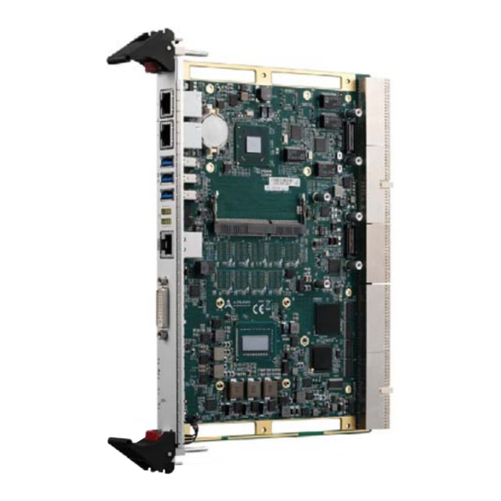
- Page 1 6U CompactPCI® 3rd Generation Intel® Core™ i7 Processor Blade User’s Manual Manual Rev.: 0.10 preliminary Revision Date: April 17, 2015 Part No: 50-15101-1010 Advance Technologies; Automate the World.
- Page 2 Revision History Revision Release Date Description of Change(s) 0.10 2015/04/17 Preliminary release...
-
Page 3: Preface
Preface Copyright 2015 ADLINK Technology Inc. This document contains proprietary information protected by copy- right. All rights are reserved. No part of this manual may be repro- duced by any mechanical, electronic, or other means in any form without prior written permission of the manufacturer. - Page 4 Conventions Take note of the following conventions used throughout this manual to make sure that users perform certain tasks and instructions properly. Additional information, aids, and tips that help users perform tasks. NOTE: NOTE: Information to prevent minor physical injury, component dam- age, data loss, and/or program corruption when trying to com- plete a task.
-
Page 5: Table Of Contents
Overview................1 Features................3 Block Diagram ..............4 Product List................5 Package Contents ............... 6 2 Specifications ..............7 cPCI-6525 Blade Specifications .......... 7 I/O Connectivity ..............9 Power Requirements ............10 3 Functional Description ............ 13 Processors................. 13 Chipset................15 Intel®... - Page 6 Front Panel ............21 Connector Pin Assignments..........22 Buttons, Switches and Jumpers......... 33 5 Checkpoints & Beep Codes ..........37 Checkpoint Ranges............37 Standard Checkpoints............37 OEM-Reserved Checkpoint Ranges........46 Important Safety Instructions..........47 Getting Service ..............49 Table of Contents...
-
Page 7: List Of Figures
List of Figures Figure 1-1: cPCI-6525 Functional Block Diagram......4 Figure 4-1: cPCI-6525 Board Layout - Front........19 Figure 4-2: cPCI-6525 Board Layout - Back ........20 Figure 4-3: cPCI-6525 Front Panel ..........21 List of Figures... - Page 8 This page intentionally left blank. viii List of Figures...
-
Page 9: List Of Tables
List of Tables Table 2-1: cPCI-6525 Blade Specifications ........7 Table 2-2: cPCI-6525 I/O Connectivity ..........9 Table 4-1: DVI-I Connector Pin Definition........24 List of Tables... - Page 10 This page intentionally left blank. List of Tables...
-
Page 11: Introduction
(total memory capacity up to 16GB). Graphics is integrated in the Intel processor with one DVI-I port on the front panel switchable to rear IO. The cPCI-6525 has two GbE control- lers (Intel® 82574IT) providing two GbE ports on the front panel (switchable to rear) and two Intel®... - Page 12 The cPCI-6525 supports operation in both a system slot and in a peripheral slot as a standalone blade. The cPCI-6525 is compliant with the PICMG 2.9 specification and supports system manage- ment functions based on the Intelligent Platform Management Interface (IPMI) as well as hardware monitoring of physical char- acteristics such as CPU and system temperature, DC voltages and power status.
-
Page 13: Features
1.2 Features 6U CompactPCI® processor blade in 4HP width form factor Quad-core 3rd Generation Intel® Core™ i7-3615QE 2.3GHz, 6MB L3 Cache, 45W TDP, FCBGA package Mobile Intel® QM77 Express Chipset (Intel® BD82QM77 PCH) Dual channel DDR3-1066/1333 ECC SDRAM up to 16GB,... -
Page 14: Block Diagram
PCIe x16 DVI 2/3 or 2x PCIe x8 SATA4 GPIO COM6 PCIe x1 PCIe Switch PCIe x1 PI7C9X130 Intel Intel KB/MS 82574IT 82574IT COM2/3/5 PCI 64b/66M PCIe x4 IPMB 0/1 GbE3 GbE4 J1/J2 J3/J4/J5 Figure 1-1: cPCI-6525 Functional Block Diagram Introduction... -
Page 15: Product List
1.4 Product List Processor Blade cPCI-6525: 4HP width (single-slot) 6U CompactPCI Pro- cessor Blade Rear Transition Module cPCI-R66S0: 6U 8HP width RTM with DVI-D, 1x COM, 3x USB, 4x GbE, 4x eSAS/SATA, 4x iSAS/SATA, PS/2 KB/MS and Line-in/out cPCI-R66N0: 6U 8HP width RTM with DVI-I, DVI-D, 1x COM, and 1x USB, 2x GbE (RJ-45);... -
Page 16: Package Contents
1.5 Package Contents The cPCI-6525 is packaged with the following components. If any of the items on the contents list are missing or damaged, retain the shipping carton and packing material and contact the dealer for inspection. Please obtain authorization before returning any prod- uct to ADLINK. -
Page 17: Specifications
• AMI EFI BIOS, 64Mbit SPI flash memory Gigabit • Two front panel GbE ports from Intel® 82579LM and Ethernet 82574IT, switchable to rear • Two rear IO GbE 10/100/1000BASE-T ports by Intel 82574IT GbE controller (PICMG 2.16 support) Table 2-1: cPCI-6525 Blade Specifications Specifications... - Page 18 • Storage Temperature: -40°C to 85°C • Humidity: 95% non-condensing • Shock: 15G peak-to-peak, 11ms duration, non-operating • Vibration : Operating 2 Grms, 5-500Hz, each axis w/o hard drive • CE EN55022 • FCC Class A Table 2-1: cPCI-6525 Blade Specifications Specifications...
-
Page 19: I/O Connectivity
SATA — — User LEDs — — General Purpose LEDs — — Reset button — — Table 2-2: cPCI-6525 I/O Connectivity Notes: 1. Signals are passed through to the RTM. Available functions are dependent on the specific RTM selected. Specifications... -
Page 20: Power Requirements
2.3 Power Requirements In order to guarantee a stable functionality of the system, it is rec- ommended to provide more power than the system requires. An industrial power supply unit should be able to provide at least twice as much power as the entire system requires of each voltage. - Page 21 Power Consumption This section provides information on the power consumption of the cPCI-6525 when using Intel® Core™ i7 processors with 4GB DDR3- 1333 soldered memory and onboard ADLINK ASD25 64GB SATA SSD. Power consumption at 100% CPU usage was measured by run- ning Intel Thermal Analysis Tool 4.3.
- Page 22 This page intentionally left blank. Specifications...
-
Page 23: Functional Description
Functional Description The following sections describe the cPCI-6525 features and functions. 3.1 Processors The 3rd Generation Intel® Core™ i7 Processor is the next genera- tion of 64-bit, multi-core mobile processors built on 22-nanometer process technology. Based on a new micro-architecture, the pro- cessor is designed for a two-chip platform. - Page 24 Supported Technologies Intel® Virtualization Technology for Directed I/O (Intel® VT-d) Intel® Virtualization Technology (Intel® VT-x) Intel® vPro Technology (Intel® VT) Intel® Trusted Execution Technology (Intel® TXT) Intel® Hyper-Threading Technology Intel® 64 Architecture Intel® Turbo Boost Technology 2.0 AES New Instructions Intel®...
-
Page 25: Chipset
3.2 Chipset The cPCI-6525 incorporates the Intel® QM77 Platform Controller Hub (PCH). Intel® QM77 Platform Controller Hub PCI Express Base Specification, Revision 2.0 support for up to eight ports with transfer rate up to 5 GT/s Supports dual display ACPI Power Management Logic Support, Revision 4.0a... -
Page 26: Intel® Turbo Boost Technology
3.3 Intel® Turbo Boost Technology Intel Turbo Boost Technology is a feature that allows the processor to opportunistically and automatically run faster than its rated operating core and/or render clock frequency when there is suffi- cient power headroom, and the product is within specified temper- ature and current limits. -
Page 27: Tpm
IC. If the data is not matched, the IC may be blocked. 3.7 Battery The cPCI-6525 is provided with a 3.0V “coin cell” lithium battery for the Real Time Clock (RTC). The lithium battery must be replaced with an identical battery or a battery type recommended by the manufacturer. - Page 28 This page intentionally left blank. Functional Description...
-
Page 29: Board Interfaces
SATA drive connector SW_COMDEG1 Reserved for debug CN13/CN14 GbE ports SW_IPMCDEG1 Reserved for debug CN21 DVI connector SW_MOD1 IPMC mode switch CN22 CFast adapter connector SW_COMPW1 Reserved for debug CN23 BIOS write protect Figure 4-1: cPCI-6525 Board Layout - Front Board Interfaces... -
Page 30: Board Layout - Back
4.2 Board Layout - Back SW_8 SW_11 Figure 4-2: cPCI-6525 Board Layout - Back RGB to front/rear switch SW11 GbE to front/rear switch Board Interfaces... -
Page 31: Cpci-6525 Front Panel
USB 3.0 Button Ó Ó Ò Ò Ð Ð Ì Ì Status LEDs User LEDs Figure 4-3: cPCI-6525 Front Panel Status LEDs Color Condition Indication System is off Power System is on Green Fail to power on Blink (payload power failure) -
Page 32: Connector Pin Assignments
4.4 Connector Pin Assignments See “Board Layout - Front” on page 19 for connector locations. Front Panel Connectors Gigabit Ethernet Connectors (CN13/CN14, RJ-45) Pin # GbE Signal LAN_TX0+ LAN_TX0- LAN_TX1+ LAN_TX2+ LAN_TX2- LAN_TX1- Speed Activity LAN_TX3+ LAN_TX3+ Speed LED Activity LED Status (Green/Amber) (Amber) - Page 33 COM1 (CN7, RJ-45) Pin # RS-232 RS-422 RS-485 DCD# Data- RTS# — — DSR# — — — Data+ — — CTS# — — DTR#L — COM1 RJ-45 to DB-9 Cable Pin # RS-232 RS-422 RS-485 DCD# Data- Data+ —...
- Page 34 USB 3.0 Connectors (CN6, CN10, CN15) Pin # Signal Name Data- Data+ RX_N RX_P TX_N TX_P DVI-I Connector Pin # Signal Pin # Signal TMDS Data2- Hot Plug Detect TMDS Data2+ TMDS Data0- TMDSData0+ DDC Clock [SCL] DDC Data [SDA] Analog vertical sync TMDS Clock + TMDS Data1-...
- Page 35 Onboard Connectors SATA Connector on DB-LSATA Pin # Signal Signal Power Reserved P13~P15 Board Interfaces...
- Page 36 CFast Socket (on DB-CFAST) Pin # Signal Name Ground SATA_TX-P SATA_TX-N Ground SATA_RX-N SATA_RX-P Ground CFast_CDI Ground Ground CFast_LED1 CFast_LED2 P3V3 P3V3 Ground Ground CFast_CDO Board Interfaces...
- Page 37 DB-LSATA/DB-CFAST Connector (CN9, CN22) Signal Name Pin # Pin # Signal Name P3V3 P3V3 P3V3 P3V3 P12V CFAST_CDI P12V CFAST_CDO P12V SATA_TXN0 SATA_TXP0 SATA_RXN0 SATA_RXP0 Board Interfaces...
- Page 38 CompactPCI J1 Connector Pin Assignment REQ64# ENUM# +3.3V V(I/O) ACK64# P3V3 CPCI_AD4 CPCI_AD3 CPCI_AD2 CPCI_AD7 P3V3 CPCI_AD6 CPCI_AD5 P3V3 CPCI_AD9 CPCI_AD8 CPCI_M66EN CPCI_CBE-L0 GND CPCI_AD12 CPCI_AD11 CPCI_AD10 P3V3 CPCI_AD15 CPCI_AD14 CPCI_AD13 CPCI_SERR-L P3V3 CPCI_PAR CPCI_CBE-L1 GND P3V3 IPMB_CLK IPMB_DAT CPCI_PERR-L GND GND CPCI_DEVSEL-L CPCI_STOP-L CPCI_LOCK-L GND P3V3...
- Page 39 CompactPCI J2 Connector Pin Assignment CLK6 CLK5 IPMB_DAT IPMB_CLK RSTBTN# REQ6# GNT6# DEG# FAL# REQ5# GNT5# AD35 AD34 AD33 AD32 AD38 V(I/O) AD37 AD36 AD42 AD41 AD40 AD39 AD45 V(I/O) AD44 AD43 AD49 AD48 AD47 AD46 AD52 V(I/O) AD51...
- Page 40 CompactPCI J3 Pin Assignment Pin Z 19 GND P12V 18 GND LAN4_TXD1+ LAN4_TXD0- LAN4_TXD2+ LAN4_TXD2- 17 GND LAN4_TXD1+ LAN4_TXD1- LAN4_TXD3+ LAN4_TXD3- 16 GND LAN3_TXD0+ LAN3_TXD0- LAN3_TXD2+ LAN3_TXD2- 15 GND LAN3_TXD1+ LAN3_TXD1- LAN3_TXD3+ LAN3_TXD3- 14 GND USB-OC45# USB-OC67# USB-OC67# USB-OC89# USB-OC89# 13 GND USB8-P USB8-N...
- Page 41 CompactPCI J4 Connector Pin Assignment PLTRST PCIE_TXP15 PCIE_WAKE-L GND _PCIEX16 PCIE_R PCIE_TXN15 XP13 PCIE_R PCIE_TXP13 PCIE_RXP15 XN13 PCIE_TXN13 PCIE_TXP14 PCIE_RXP14 PCIE_RXN15 PCIE_TX PCIE_TXN14 PCIE_RXN14 PCIE_TX PCIE_TXP10 PCIE_RXP12 PCIE_TXN10 PCIE_TXP11 PCIE_RXP10 PCIE_RXN12 PCIE_R PCIE_TXN11 PCIE_RXN10 PCIE_R PCIE_TXP8 PCIE_RXP11 PCIE_TXN8 PCIE_TXP9...
- Page 42 CompactPCI J5 Pin Assignment 22 GND LAN2_TXDP0 LAN2_TXDN0 LAN2_TXDP2 LAN2_TXDN2 21 GND LAN2_TXDP1 LAN2_TXDN1 LAN2_TXDP3 LAN2_TXDN3 20 GND LAN1_TXDP0 LAN1_TXDN0 LAN1_TXDP2 LAN1_TXDN2 19 GND LAN1_TXDP1 LAN1_TXDN1 LAN1_TXDP3 LAN1_TXDN3- 18 GND TMDSD_CLK+ TMDSD_CLK- 17 GND TMDSD_DATA1+ TMDSD_DATA1- COM5_TX COM5_RX 16 GND DVI_SDA_D DVI_SCL_D DVI_HPD_D...
-
Page 43: Buttons, Switches And Jumpers
4.5 Buttons, Switches and Jumpers See “cPCI-6525 Front Panel” on page 21 and “Board Layout - Front” on page 19 for switch locations. System Reset Button The cPCI-6525 has a system reset button on the front panel. See “cPCI-6525 Front Panel” on page 21 for the button location. - Page 44 COM1 Mode Switch (SW12) Switch SW12 sets the mode of the COM1 port on the front panel. Mode RS-232 (default) RS-422 RS-485 IPMC Mode Switch (SW_MOD1) Switch SW_MOD1 is a multi purpose switch that allows users to define the blade operating mode. All are set to OFF by default. Pin# Status Description Reserved...
- Page 45 RGB to Front/Rear Switch (SW8) Pin# Status Description RGB to front (default) RGB to rear Normal (default) Debug GbE to Front/Rear Switch (SW11) Pin# Status Description GbE1 to rear GbE1 to front (default) GbE2 to rear GbE2 to front (default)
- Page 46 Reserved Switches Switches SW_COMDEG1 and SW_IPMCDEG1 are reserved and their settings should not be altered unless instructed by ADLINK. The default settings are as follows: SW_COMDEG1: 1, 2 ON; 3, 4 OFF SW_IPMCDEG1: All OFF SW_COMPW1: ON (short 2-3) BIOS Write Protection Jumper (CN23) Mode Jumper Setting No BIOS protection...
-
Page 47: Checkpoints & Beep Codes
Checkpoints & Beep Codes 5.1 Checkpoint Ranges Status Code Range Description 0x01 – 0x0B SEC execution 0x0C – 0x0F SEC errors PEI execution up to and including memory 0x10 – 0x2F detection 0x30 – 0x4F PEI execution after memory detection 0x50 –... - Page 48 Status Code Description North Bridge initialization after microcode 0x08 loading South Bridge initialization after microcode 0x09 loading 0x0A OEM initialization after microcode loading 0x0B Cache initialization SEC Error Codes 0x0C – 0x0D Reserved for future AMI SEC error codes 0x0E Microcode not found 0x0F Microcode not loaded...
- Page 49 Status Code Description Pre-memory South Bridge initialization (South 0x1A Bridge module specific) Pre-memory South Bridge initialization (South 0x1B Bridge module specific) Pre-memory South Bridge initialization (South 0x1C Bridge module specific) 0x1D – 0x2A OEM pre-memory initialization codes Memory initialization. Serial Presence Detect...
- Page 50 Status Code Description Post-Memory South Bridge initialization is 0x3B started Post-Memory South Bridge initialization (South 0x3C Bridge module specific) Post-Memory South Bridge initialization (South 0x3D Bridge module specific) Post-Memory South Bridge initialization (South 0x3E Bridge module specific) 0x3F-0x4E OEM post memory initialization codes 0x4F DXE IPL is started PEI Error Codes...
- Page 51 Status Code Description 0xE3 OS S3 wake vector call 0xE4-0xE7 Reserved for future AMI progress codes S3 Resume Error Codes 0xE8 S3 Resume Failed 0xE9 S3 Resume PPI not Found 0xEA S3 Resume Boot Script Error 0xEB S3 OS Wake Error...
- Page 52 PEI Beep Codes # of Beeps Description Memory not Installed Memory was installed twice (InstallPeiMemory routine in PEI Core called twice) Recovery started DXEIPL was not found DXE Core Firmware Volume was not found Recovery failed S3 Resume failed Reset PPI is not available DXE Phase Status Code Description...
- Page 53 Status Code Description North Bridge DXE initialization (North Bridge 0x6F module specific) 0x70 South Bridge DXE initialization is started 0x71 South Bridge DXE SMM initialization is started 0x72 South Bridge devices initialization South Bridge DXE Initialization (South Bridge 0x73...
- Page 54 Status Code Description 0xA0 IDE initialization is started 0xA1 IDE Reset 0xA2 IDE Detect 0xA3 IDE Enable 0xA4 SCSI initialization is started 0xA5 SCSI Reset 0xA6 SCSI Detect 0xA7 SCSI Enable 0xA8 Setup Verifying Password 0xA9 Start of Setup Reserved for ASL (see ASL Status Codes 0xAA section below) 0xAB...
- Page 55 Status Code Description Some of the Architectural Protocols are not 0xD3 available 0xD4 PCI resource allocation error. Out of Resources 0xD5 No Space for Legacy Option ROM 0xD6 No Console Output Devices are found 0xD7 No Console Input Devices are found...
-
Page 56: Oem-Reserved Checkpoint Ranges
ACPI/ASL Checkpoints Status Code Description 0x01 System is entering S1 sleep state 0x02 System is entering S2 sleep state 0x03 System is entering S3 sleep state 0x04 System is entering S4 sleep state 0x05 System is entering S5 sleep state 0x10 System is waking up from the S1 sleep state 0x20... -
Page 57: Important Safety Instructions
Important Safety Instructions For user safety, please read and follow all instructions, WARNINGS, CAUTIONS, and NOTES marked in this manual and on the associated equipment before handling/operating the equipment. Read these safety instructions carefully. Keep this user’s manual for future reference. - Page 58 Never attempt to fix the equipment. Equipment should only be serviced by qualified personnel. A Lithium-type battery may be provided for uninterrupted, backup or emergency power. Risk of explosion if battery is replaced with one of an incorrect type. Dispose of used batteries appropriately. WARNING: Equipment must be serviced by authorized technicians when:...
-
Page 59: Getting Service
San Jose, CA 95138, USA Tel: +1-408-360-0200 Toll Free: +1-800-966-5200 (USA only) Fax: +1-408-360-0222 Email: info@adlinktech.com ADLINK Technology (China) Co., Ltd. Address: (201203) 300 Fang Chun Rd., Zhangjiang Hi-Tech Park Pudong New Area, Shanghai, 201203 China Tel: +86-21-5132-8988 Fax: +86-21-5132-3588 Email: market@adlinktech.com... - Page 60 84 Genting Lane #07-02A, Cityneon Design Centre Singapore 349584 Tel: +65-6844-2261 Fax: +65-6844-2263 Email: singapore@adlinktech.com ADLINK Technology Singapore Pte. Ltd. (Indian Liaison Office) Address: #50-56, First Floor, Spearhead Towers Margosa Main Road (between 16th/17th Cross) Malleswaram, Bangalore - 560 055, India Tel: +91-80-65605817, +91-80-42246107 Fax:...
Need help?
Do you have a question about the cPCI-6525 and is the answer not in the manual?
Questions and answers