
Related Manuals for ADLINK Technology cPCI-3520 Series


Summary of Contents for ADLINK Technology cPCI-3520 Series
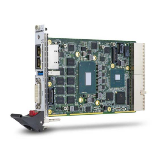
- Page 1 Series Performance 3U CompactPCI® Intel® Xeon® E Processor Blade User’s Manual Manual Rev.: 0.3 Preliminary Revision Date: December 28, 2021 Part No: 50M-00036-1000...
- Page 2 Revision History Revision Release Date Description of Change(s) 2021-07-28 Preliminary release 2021-09-17 Update specifications, add GPIO Correct cPCI-3520M 100-pin I/O Connector 2021-12-28 DVD-D spec; I/O Connectivity Table Revision History...
-
Page 3: Preface
Preface Copyright © 2021 ADLINK Technology, Inc. This document contains proprietary information protected by copy- right. All rights are reserved. No part of this manual may be repro- duced by any mechanical, electronic, or other means in any form without prior written permission of the manufacturer. - Page 4 California Proposition 65 Warning WARNING: This product can expose you to chemicals including acrylamide, arsenic, benzene, cadmium, Tris(1,3-dichloro-2-propyl)phosphate (TDCPP), 1,4-Diox- ane, formaldehyde, lead, DEHP, styrene, DINP, BBP, PVC, and vinyl materials, which are known to the State of California to cause cancer, and acrylamide, benzene, cadmium, lead, mercury, phthalates, toluene, DEHP, DIDP, DnHP, DBP, BBP, PVC, and vinyl materials, which are known to the State of California to cause...
-
Page 5: Table Of Contents
cPCI-3520 Table of Contents Revision History..............ii Preface ..................iii List of Figures ............... vii List of Tables................ix 1 Introduction ................ 1 Overview................1 Features................2 Model Number Decoder............3 Package Contents ............... 5 2 Specifications ..............7 cPCI-3520 Processor Blade Specifications ......7 cPCI-R3P00(T) RTM Specifications ........ - Page 6 Series Board Layout ........29 cPCI-3520 Blade Assembly Layout ........31 cPCI-3520D Blade Assembly Layout......... 32 cPCI-3520G Blade Assembly Layout......... 33 cPCI-3520L Blade Assembly Layout ......... 34 cPCI-3520M Blade Assembly Layout ........ 35 cPCI-3520S Blade Assembly Layout ......... 36 cPCI-3520 Series Faceplate Layout ........
-
Page 7: List Of Figures
Figure 2-6: cPCI-R3P00 RTM Functional Block Diagram ....17 Figure 2-7: cPCI-R3P00T RTM Functional Block Diagram....18 Figure 4-1: cPCI-3520 Series Board Layout (component side) ..29 Figure 4-2: cPCI-3520 Series Board Layout (solder side) ....30 Figure 4-3: cPCI-3520 Blade Assembly Layout ....... 31 Figure 4-4: cPCI-3520D Blade Assembly Layout...... - Page 8 This page intentionally left blank. viii List of Figures...
-
Page 9: List Of Tables
cPCI-3520 List of Tables Table 2-1: cPCI-3520 Processor Blade Specifications ..... 7 Table 2-2: cPCI-R3P00(T) RTM Specifications ......11 Table 2-3: cPCI-3520 I/O Connectivity ........... 19 Table 4-1: cPCI-3520 Faceplate System LED Descriptions ... 39 Table 4-2: USB 2.0 Pin Definition ........... 42 Table 4-3: VGA Pin Definition ............ - Page 10 This page intentionally left blank. List of Tables...
-
Page 11: Introduction
Intel® Core™ and Intel® Celeron® G processor (formerly Coffee Lake-H) with Mobile Intel® CM246 Chipset. The cPCI-3520 Series is a 3U CompactPCI blade available in sin- gle-slot (4HP), dual-slot (8HP) or triple-slot (12HP) width form fac- tors with various daughter boards to provide a broad range of I/O requirements. -
Page 12: Features
system health monitoring. A GbE port on the faceplate supports Intel® AMT 9.0 for remote monitoring. 1.2 Features 3U CompactPCI blade in 4HP, 8HP or 12HP width form factor Intel® Xeon® E, 8th/9th Gen Intel® Core™ Processor Graphics and memory controllers integrated in processor Dual channel DDR4-2666 soldered SDRAM with ECC, up to 32GB 32-bit, 33/66MHz CompactPCI Interface based on PCI specifi-... -
Page 13: Model Number Decoder
cPCI-3520 1.3 Model Number Decoder Blades cPCI-EX 3520 9850HL 32G / S32 (A) Operating Temperature Code Blank = -20°C to +70°C EX= -40°C to +85°C (for CPUs with TDP 25W only) (B) Configuration Code Blank = Single slot width with CFast socket, 1x DVI-I, 1x USB 3.0, 2x GbE D = Dual slot width with CFast socket, 1x DVI-I, 1x USB 3.0, 2x GbE on layer 1;... - Page 14 (C) CPU Code 2276ML= 6-core Intel® Xeon® E-2276ML w/ ECC 9850HL = 6-core Intel® Core™ i7-9850HL 8400HL = 4-core Intel® Core™ i5-8400H 9100HL= 4-core Intel® Core™ i3-9100HL w/ ECC (D) Memory Size Code M8 = 8GB DDR3L-2666 soldered SDRAM M16 = 2x 8GB DDR3L-2666 soldered SDRAM M32 = 2x 16GB DDR4-2666 soldered SDRAM (E) Storage Board Code Blank = Default with CFast socket...
-
Page 15: Package Contents
Please obtain authorization before returning any product to ADLINK. The packing contents of cPCI-3520 Series non-standard configurations will vary depending on customer requests. Processor Blade... - Page 16 Blade Optional Accessories 2.5” SATA drive installation kit (P/N 58-00176-0000) Y-cable for PS/2 combo port (P/N 30-01016-2000) RJ-45 to DB-9 COM adapter cable (P/N 30-01020-0200) DisplayPort to DVI adapter cable (P/N 30-01120-0000) DisplayPort to VGA adapter cable (P/N 30-01119-0000) DisplayPort to HDMI adapter cable (P/N 30-01121-0000) USB 3.0 Type A male-to-female extension cable (P/N: 30-01175-0000) SCSI 100-pin IO cable: 2x DVI-D female, 2x DB9 male,...
-
Page 17: Specifications
cPCI-3520 Specifications 2.1 cPCI-3520 Processor Blade Specifications CompactPCI® • PICMG® 2.0 CompactPCI® Rev. 3.0 Standards • PICMG® 2.9 System Management Rev. 1.0 (IPMI v1.5) Mechanical • Standard 3U CompactPCI® • Board size: 100mm x 160mm • Single slot (4HP, 20.32mm); Dual slot (8HP, 40.64mm); Triple slot (12HP, 60.96 mm) •... - Page 18 Graphics • Integrated on Intel® Core™ processor • DVI-I port on faceplate, VGA switchable to J2 (RTM) by BIOS setting • Analog monitor support up to QXGA 2048x1536 @75Hz, 32-bit • Two DisplayPorts on faceplate with resolution up to 2560x1440 @60Hz (cPCI-3520G only) •...
- Page 19 cPCI-3520 Environmental • Operating Temperature (with forced air flow) Standard: -20°C to 70°C Extreme temperature: -40°C to +85°C • Storage Temperature: -50°C to 100°C • Humidity: 95% @60°C non-condensing • Shock: 20G peak-to-peak, 11ms duration, non-operating • Vibration : 2Grms, 5-500Hz, each axis, operating (w/o hard drive) •...
- Page 20 Faceplate I/O 8HP cPCI-3520S (cont’d) • 1x USB 3.0 ports • 2x 10/100/1000BASE-T Ethernet ports • 1x DVI-I port • PMC/XMC site • 12HP cPCI-3520P • 1x USB 3.0 ports • 2x 10/100/1000BASE-T Ethernet ports • 1x DVI-I port • 2x USB 2.0 ports •...
-
Page 21: Cpci-R3P00(T) Rtm Specifications
cPCI-3520 2.2 cPCI-R3P00(T) RTM Specifications Mechanical Board Size • cPCI-R3P00: 100mm x 50mm • cPCI-R3P00T: 100mm x 80mm Dual-slot (8HP, 40.64mm) (optional single slot upon request) Gigabit • cPCI-R3P00: Two GbE ports switched from cPCI-3520 2x Ethernet Intel® Ethernet Controllers I210 •... -
Page 22: Block Diagrams
2.3 Block Diagrams cPCI-3520 Processor Blade Faceplate Intel® Intel® BIOS ECC, up to 16GB I219 I210 USB 3.0 CFast ECC, up to 16GB Battery mSATA PCIe x1 PCIe x1 SATA DDR4-2133 ® Intel CM246 Chipset Intel ® Coffee Lake-H SATA, HDA, DP1/DVI 2x USB 3.0 2x PCIe x1... - Page 23 cPCI-3520 cPCI-3520D Daughter Board (DB-3610L2) USB x2 Conn. Line-in, Line-out Codec SATA0 2.5” HDD/SDD PS/2, KB/MS Figure 2-2: cPCI-3520D Daughter Board Functional Block Diagram Specifications...
- Page 24 cPCI-3520G Daughter Board (DB-3970L2) Conn. DVI/DP SATA0 2.5” HDD/SSD DVI/DP COM1 COM2 10-pin KB/MS Figure 2-3: cPCI-3520G Daughter Board Functional Block Diagram Specifications...
-
Page 25: Figure 2-4: Cpci-3520L Daughter Board Functional Block Diagram
cPCI-3520 cPCI-3520L Daughter Board (DB-LAN2-S) USB x1 Conn. USB x1 Horizontal Type A RS232/422/485 SATA0 2.5” HDD GbE 3 82574L GbE 4 82574L Figure 2-4: cPCI-3520L Daughter Board Functional Block Diagram Specifications... - Page 26 cPCI-3520M Daughter Board (DB-Max) 100-pin Conn. high Line-in, Line-out density connector 2x DVI-D 2.5” HDD/Slim SATA0 2x USB 2.0 2x COM (RS232/422/485) KB/MS Figure 2-5: cPCI-3520M Daughter Board Functional Block Diagram Specifications...
-
Page 27: Figure 2-6: Cpci-R3P00 Rtm Functional Block Diagram
cPCI-3520 cPCI-R3P00 RTM COM (Tx, Rx) 2x USB GbE 1/2 SATA3/4/5 7 pin 7 pin 7 pin U SB3 RS232/422/485 FT2 32R Figure 2-6: cPCI-R3P00 RTM Functional Block Diagram Specifications... -
Page 28: Figure 2-7: Cpci-R3P00T Rtm Functional Block Diagram
cPCI-R3P00T RTM COM (Tx, Rx) 2x USB PC Ie x4 GbE 3/4 82580DB SATA3/4/5 7 pin 7 pin 7 pin U SB3 RS232/422/485 FT2 32R Figure 2-7: cPCI-R3P00T RTM Functional Block Diagram Specifications... -
Page 29: I/O Connectivity Table
cPCI-3520 2.4 I/O Connectivity Table cPCI-3520 cPCI-3520D cPCI-3520G cPCI-3520L (4HP) (8HP) (8HP) (8HP) Function Faceplate Onboard Faceplate Onboard Faceplate Onboard Faceplate Onboard 2 (RJ-45) 2 (RJ-45) 2 (RJ-45) 4 (RJ-45) 1 (3.0) 1 (3.0) 1 (3.0) 1 (3.0) 2 (2.0) 1 (2.0) 1 (2.0) 1 (DB9) - Page 30 cPCI-3520M cPCI-3520S cPCI-3520P R3P00(T) (8HP) (8HP) (12HP) (RTM) Function Faceplate Onboard Faceplate Onboard Faceplate Onboard Faceplate Onboard 2 (RJ-45) 2 (RJ-45) 2 (RJ-45) 2 (RJ-45) 1 (3.0) 1 (3.0) 1 (3.0) 2 (2.0) 2 (2.0) 2 (2.0) 2 (DB9) 1 (DB9) 2 (DB9) 1 (DVI-I) Display...
-
Page 31: Power Requirements
cPCI-3520 2.5 Power Requirements In order to guarantee a stable functionality of the system, it is rec- ommended to provide more power than the system requires. An industrial power supply unit should be able to provide at least twice as much power as the entire system requires of each voltage. - Page 32 Power Consumption This section provides information on the power consumption of cPCI-3520 Series when using the Intel® Core™ i7 processor with 32GB DDR4-2666 ECC soldered memory and onboard 64GB SATA flash disk. The cPCI-3520 is powered by 5V and 3.3V. Power con- sumption at 100% CPU usage was measured using the Intel Ther- mal Analysis Tool (TAT).
-
Page 33: Functional Description
Functional Description The following sections describe the cPCI-3520 Series features and functions. 3.1 Processors The Mobile 8th/9th Generation Intel® Core™ Processor Family, Intel® Xeon® E Processor, and Celeron® Processor G Series are 64-bit, multi-core mobile processor built on 14 nanometer process technology. - Page 34 Supported Technologies Xeon® Core™ i7- Core™ i5- Core™ i3- Celeron® Features E-2276ML 9850HL 8400H 9100HL G4930E Intel® Virtualization Technology for Directed I/O (Intel® VT-d) Intel® Virtualization Technology (Intel® VT-x) Intel® VT-x with Extended Page Tables (EPT) Intel® Hyper-Threading Technology Intel® 64 Architecture Execute Disable Bit Intel®...
-
Page 35: Chipset
cPCI-3520 3.2 Chipset The Mobile Intel® C240 Series Chipset provides extensive I/O support. Functions and capabilities include: PCI Express Base Specification, Revision 3.0 ACPI Power Management Logic Support, Revision 4.0a Interrupt controller and timer functions Integrated Serial ATA host controller 3.2, supports data transfer rates up to 6Gb/s on all ports XHCI USB 3.1 Controller Integrated 10/100/1000 Gigabit Ethernet MAC with System... -
Page 36: Intel® Hyper-Threading Technology
ature and current limits. The Intel Turbo Boost Technology feature is designed to increase performance of both multi-threaded and single-threaded workloads. The processor supports a Turbo mode where the processor can use the thermal capacity associated with package and run at power levels higher than TDP power for short durations. -
Page 37: Battery
cPCI-3520 The key features the Trusted Platform Module (TPM) offers are: Compliant to TPM 2.0 Rev. 01.16 Pin compatible to SLB9660 Low Pin Count (LPC) to allow easy system integration TCG and Common Criteria certified with EAL4+ FIPS 140-2 certified FW available via FW update Full personalization with Endorsement Key (EK) and EK certificate 1280 byte I/O buffer... - Page 38 This page intentionally left blank. Functional Description...
-
Page 39: Board Interfaces
Processor CompactPCI connector J1 Layer-2 daughter board CompactPCI connector J2 connector (UHM/HM) Storage daughter board LAN1 Dual Ethernet connectors connector cPCI-3520G daughter USB1 USB port board connector DVI1 DVI connector Figure 4-1: cPCI-3520 Series Board Layout (component side) Board Interfaces... -
Page 40: Figure 4-2: Cpci-3520 Series Board Layout (Solder Side)
Reset Button Figure 4-2: cPCI-3520 Series Board Layout (solder side) Board Interfaces... -
Page 41: Cpci-3520 Blade Assembly Layout
cPCI-3520 4.2 cPCI-3520 Blade Assembly Layout This section describes the final assembly layout of the single slot cPCI-3520 Blade. Heatsink Figure 4-3: cPCI-3520 Blade Assembly Layout Battery CompactPCI connector J1 Clear CMOS jumper CompactPCI connector J2 Board Interfaces... -
Page 42: Cpci-3520D Blade Assembly Layout
4.3 cPCI-3520D Blade Assembly Layout The dual-slot width cPCI-3520D Blade is comprised of the cPCI-3520 single-slot main board and the cPCI-3520D daughter board to expand I/O connectivity with PS/2, COM, 2x USB ports, Line-in, and Line-out ports . COM1 SATA0 USB2 2.5”... -
Page 43: Cpci-3520G Blade Assembly Layout
cPCI-3520 4.4 cPCI-3520G Blade Assembly Layout The dual-slot width cPCI-3520G Blade is comprised of the cPCI-3520 single-slot main board and the cPCI-3520G daughter board to expand I/O connectivity with PS/2, COM, USB ports, and 2x DisplayPorts. COM2 2.5” SATA HDD SATA0 COM1 cPCI-3520G... -
Page 44: Cpci-3520L Blade Assembly Layout
4.5 cPCI-3520L Blade Assembly Layout The dual-slot width cPCI-3520L Blade is comprised of the cPCI-3520 single-slot main board and the cPCI-3520L daughter board, expanding I/O connectivity with 2x LAN, COM, USB. LAN1 SATA1 2.5” SATA HDD COM1 cPCI-3520L daughter board USB1 LAN1 GbE RJ-45 ports... -
Page 45: Cpci-3520M Blade Assembly Layout
cPCI-3520 4.6 cPCI-3520M Blade Assembly Layout The dual-slot width cPCI-3520M Blade is comprised of the cPCI-3520 single-slot main board and the cPCI-3520M daughter board, expanding I/O connectivity with a 100-pin high density con- nector. SATA0 cPCI-3520M daughter board 100-pin high density SATA0 22-pin SATA connector connector Figure 4-7: cPCI-3520M Blade Assembly Layout... -
Page 46: Cpci-3520S Blade Assembly Layout
4.7 cPCI-3520S Blade Assembly Layout The dual-slot width cPCI-3520S Blade is comprised of the cPCI-3520 single-slot main board and the DB-3UMC riser card, expanding I/O connectivity with a XMC/PMC connector. DB-3UMC XMC connector JN1/JN2/JN4 PCM connectors Board Interfaces... -
Page 47: Cpci-3520 Series Faceplate Layout
4.8 cPCI-3520 Series Faceplate Layout cPCI-35 0 USB 3.0 GbE A/B Power LED WDT LED GP LED Reset Button HDD LED Thermal LED cPCI-35 0D PS/2 KB/MS Line-in Line-out USB 2.0 COM1 Reset Button Power LED GP LED DVI-I... -
Page 48: Figure 4-9: Cpci-3520L/M/S Faceplate Layout
cPCI-35 0L LAN Connector Power LED Reset Button DVI-I GP LED Thermal LED WDT LED HDD LED cPCI-35 0M 100-pin Connector Power LED Reset Button DVI-I GP LED Thermal LED WDT LED HDD LED XMC Slot cPCI-35 0S LED Definitions same as above Reset Button DVI-I... -
Page 49: Table 4-1: Cpci-3520 Faceplate System Led Descriptions
cPCI-3520 cPCI-3520P: Same faceplate as cPCI-3520D but with XMC/PMC slot on Layer 3. System LEDs Color Condition Indication System is off Power Green/ System Power ready (PWGD) Green Post OK No Watchdog event Orange Blinking Watchdog event alert No CF/CFast/mSATA/SATA activity Drive Blue Data read/write in process for CF/CFast/... -
Page 50: Cpci-R3P00(T) Rtm Board Layout
4.9 cPCI-R3P00(T) RTM Board Layout LAN1/2 USB1 SATA2 USB10 SATA SATA VGA1 COM4 COM5* RS-232/422/485 port LAN1/2 Dual Ethernet ports (converted from USB) COM4 RS-232 port (Tx, Rx only) VGA1 VGA port SATA2/3/4 SATA ports USB1/10 USB ports CompactPCI connector (cPCI-R3P00 is 50mm deep and cPCI-R3P00T is 80mm deep) Figure 4-10: cPCI-R3P00(T) RTM Board Layout *COM5 is incorrectly labeled COM3 on the A1 vers. -
Page 51: Cpci-R3P00(T) Rtm Faceplate
cPCI-3520 4.10 cPCI-R3P00(T) RTM Faceplate COM4 COM5 USBx2 GbE x2 Figure 4-11: cPCI-R3P00(T) RTM Faceplate Board Interfaces... -
Page 52: Connector Pin Assignments
4.11 Connector Pin Assignments USB 2.0 Connectors Pin # Signal Name UV0- UV0+ Table 4-2: USB 2.0 Pin Definition USB 3.0 Connectors Pin # Signal Name USB3.0_P5VA USB2_CMAN USB2_CMAP USB3A_CMRXN USB3A_CMRXP USB3A_CMTXN USB3A_CMTXP Board Interfaces... -
Page 53: Table 4-3: Vga Pin Definition
cPCI-3520 DB-15 VGA Connector Signal Name Pin # Pin # Signal Name Green Blue N.C. +5V. N.C. CRTDATA HSYNC VSYNC CRTCLK Table 4-3: VGA Pin Definition DisplayPort Connectors Pin # Signal Pin # Signal CN_DP0_P Ground CN_DP0_N CN_DP1_P Ground CN_DP1_N CN_DP2_P Ground CN_DP2_N... -
Page 54: Table 4-5: Dvi-I Connector Pin Definition
DVI-I Connector Pin # Signal Pin # Signal TMDS Data2- Hot Plug Detect TMDS Data2+ TMDS Data0- TMDSData0+ DDC Clock [SCL] DDC Data [SDA] Analog vertical sync TMDS Clock + TMDS Data1- TMDS Clock - TMDS Data1+ Analog Red Analog Green Analog Blue Analog Horizontal Sync +5 V Power... -
Page 55: Table 4-6: Rj-45 Gbe Pin Definitions
cPCI-3520 RJ-45 Gigabit Ethernet Connectors 10BASE-T/ Pin # 1000BASE-T 100BASE-TX LAN_TX0+ LAN_TX0- LAN_TX1+ — LAN_TX2+ — LAN_TX2- LAN_TX1- — LAN_TX3+ — LAN_TX3- Table 4-6: RJ-45 GbE Pin Definitions Speed Activity Speed LED Activity LED Status (Green/Orange) (Yellow) Network link is not established or system powered off Link 10 Mbps... -
Page 56: Table 4-8: Ps/2 Keyboard/Mouse Pin Definition
PS/2 Keyboard/Mouse Connector Pin # Signal Function KBDATA Keyboard Data MSDATA Mouse Data Ground Power KBCLK Keyboard Clock MSCLK Mouse Clock Table 4-8: PS/2 Keyboard/Mouse Pin Definition cPCI-3520D/P Serial Ports COM1 Connector (DB-9) Pin # RS-232 RS-422 RS-485(+) DCD-L TXD- TXD- TXD+ TXD+... -
Page 57: Table 4-10: Cpci-3520D/P Com1 Mode Selection Switch Settings
cPCI-3520 COM1 Mode Selection Switches (SW1~SW4) These switches set the cPCI-3520D/P COM1 to RS-232 full modem, RS-422, RS-485, or RS-485+ half-duplex mode. Switches SW1~SW4 are located on the top edge of the cPCI-3520D daughter board. RS-232 full modem is set by default. -
Page 58: Table 4-11: Cpci-3520G Com1 (Rj-45) Pin Definition
cPCI-3520G Serial Ports COM1 Connector (RJ-45) Pin # RS-232 RS-422 RS-485 DCD-L — — RTS-L TXD+ TXD+ DSR-L — — TXD- TXD- RXD- — Ground — — CTS-L RXD+ — DTR-L — — RI-L — — Table 4-11: cPCI-3520G COM1 (RJ-45) Pin Definition COM1 Connector with DB-9 Adapter An RJ-45 to DB-9 adapter cable is provided to breakout the COM1 signals. -
Page 59: Table 4-13: Rs-422/485 Adapter Dongle Pin Definition
cPCI-3520 The cPCI-3520G COM1 RS-422/485 pin definitions are different from the common DB-9 pin definitions. An RS-422/485 DB-9 male-female adapter dongle allows compatibility with common NOTE: NOTE: RS-422/485 pin definitions. RS-422/485 Adapter Dongle for cPCI-3520G A DB-9 male-female adapter dongle allows compatibility with common RS-422/485 pin definitions DB-9 (Female) DB-9 (Male) -
Page 60: Table 4-15: Cpci-3520G Com2 Pin Header Definition
COM2 Pin Header Pin # RS-232 RS-422 RS-485 DCD-L — — DSR-L — — RXD- — RTS-L TXD+ TXD+ TXD- TXD- CTS-L RXD+ — DTR-L — — RI-L — — Ground — — — — Table 4-15: cPCI-3520G COM2 Pin Header Definition The COM mode settings for cPCI-3520G models are set in the BIOS: see “Output (cPCI-3520G COM1/2)”... -
Page 61: Table 4-17: Cpci-R3P00(T) Rtm Com5 Pin Definition
cPCI-3520 COM5 Connector (DB-9) The cPCI-R3P00(T) RTM COM5 RS-422/485 pin definitions are different from the common DB-9 pin definitions. An RS-422/485 DB-9 male-female adapter dongle allows compatibility with com- NOTE: NOTE: mon RS-422/485 pin definitions. See “RS-422/485 Adapter Don- gle for cPCI-3520G” on page 49 Pin # RS-232 RS-422... -
Page 62: Table 4-19: Cpci-3520M 100-Pin I/O Connector Pin Definition
cPCI-3520M 100-pin I/O Connector (CN4) Pin # Signal Pin # Signal USB9_CN-N USB9_CN-P USB1_CN-N USB1_CN-P TMDS_I2C_DATA TMDS_I2C_CLK TMDSB_DATA2B TMDSB_DATA2 TMDSB_DATA1B TMDSB_DATA1 TMDSB_DATA0B TMDSB_DATA0 TMDSB_CLKB TMDSB_CLK P5V_DVI1 TMDSB_HPD NC TMDS_I2C_DATA TMDS_I2C_CLK TMDSB_DATA2B TMDSB_DATA2 TMDSB_DATA1B TMDSB_DATA1 TMDSB_DATA0B TMDSB_DATA0 TMDSB_CLKB TMDSB_CLK P5V_DVI2 TMDSB_HPD P5V_USB_1_9 P5V_USB_1_9 P5V_USB_1_9... - Page 63 cPCI-3520 Pin # Signal Pin # Signal COM1_RXD_CN COM1_CTS-L_CN COM1_TXD_CN COM1_RTS-L_CN COM1_DTR-L_CN COM1_DSR-L_CN COM1_DCD-L_CN COM2_RXD_CN COM2_CTS-L_CN COM2_TXD_CN COM2_RTS-L_CN COM2_DTR-L_CN COM2_DSR-L_CN COM2_DCD-L_CN AGND_AU AGND_AU L_IN_R L_IN_L L_IN_JD AGND_AU HP_R HP_L HP_JD AGND_AU Table 4-19: cPCI-3520M 100-pin I/O Connector Pin Definition Board Interfaces...
-
Page 64: Table 4-20: Serial Ata Connector On Rtm
Serial ATA Connectors on RTM (CN4-R, CN5-R) Pin # Signal Table 4-20: Serial ATA Connector on RTM SATA Conn. on cPCI-3520D/G/M Daughter Board Pin # Signal Signal Power P13~P15 Table 4-21: SATA on cPCI-3520D/G/M Daughter Board Pin Def’n Board Interfaces... -
Page 65: Table 4-22: Cfast Socket Pin Definition
cPCI-3520 CFast Socket (on CFast carrier board) Pin # Signal Name Ground SATA_TX-P SATA_TX-N Ground SATA_RX-N SATA_RX-P Ground CFast_CDI Ground Ground CFast_LED1 CFast_LED2 P3V3 P3V3 Ground Ground CFast_CDO Table 4-22: CFast Socket Pin Definition Board Interfaces... -
Page 66: Table 4-23: Layer-2 Daughter Board Connector Pin Definition
Layer-2 Daughter Board Connector (CN1) Signal Name Pin # Pin # Signal Name USB2-N -12V USB2-P USB3-N HDA_SDIN0 USB3-P HDA_R_SDOUT SATA_ICH_RX-N0 HDA_R_SYNC SATA_ICH_RX-P0 HDA_R_BIT_CLK SATA_TX-P0 CK_L2_PCIE1-P SATA_TX-N0 CK_L2_PCIE1-N PCIE_TXN5 CK_L2_PCIE2-P PCIE_TXP5 CK_L2_PCIE2-N PCIE_RXN5 HDA_R_RST-L PCIE_RXP5 SPKR L2_PCIE_RST-L PCIE_RXN4 PCIE_RXP4 USB_2_3_OC-L COM1_DCD-L PCIE_TXN4 COM1_RI-L... -
Page 67: Table 4-24: Storage Daughter Board Connector Pin Definition
cPCI-3520 Storage Daughter Board Connector (CN2) Signal Name Pin # Pin # Signal Name PCH_SPKR CLK33_TPM SIO_SPKR LPC_FRAME-L TPM_RST-L CN_VCC_RTC LPC_AD3 LPC_AD2 LPC_AD1 LPC_AD0 TPM_LPCPD PCH_SERIRQ TPM_CLKRUN TPM_GPIO SATA_PCH_RX-N0 SATA_PCH_RX-P0 SATA_PCH_TX-N0 SATA_PCH_TX-P0 CFast_CDI CFast_CDO P3V3 P3V3 Table 4-24: Storage Daughter Board Connector Pin Definition Board Interfaces... -
Page 68: Table 4-25: Cpci-3520G Daughter Board Connector Pin Definition
cPCI-3520G Daughter Board Connector (CN3) Signal Name Pin # Pin # Signal Name RS232_COM2_SEL-L COM2_DCD-L COM2_RI-L COM2_CTS-L COM2_DTR-L COM2_RTS-L COM2_DSR-L COM2_SOUT COM2_SIN PCH_DDPD_AUXN PCH_DDPC_AUXN PCH_DDPD_AUXP PCH_DDPC_AUXP PCH_DDPD_0N PCH_DDPC_0N PCH_DDPD_0P PCH_DDPC_0P PCH_DDPD_1N PCH_DDPC_1N PCH_DDPD_1P PCH_DDPC_1P PCH_DDPD_2N PCH_DDPC_2N PCH_DDPD_2P PCH_DDPC_2P PCH_DDPD_3N PCH_DDPC_3N PCH_DDPD_3P PCH_DDPC_3P DDPD_CTRLCLK... -
Page 69: Table 4-26: Pmc/Xmc Daughter Board Connector Pin Definition
cPCI-3520 PMC/XMC Daughter Board Connector (on cPCI-3520D/G daughter board) Signal Name Pin # Pin # Signal Name -12V +12V CK_PCIE1_P CK_PCIE1_N PCIE_TXN2 CK_PCIE2_P PCIE_TXP2 CK_PCIE2_N PCIE_R_RXN2 PCIE_R_RXP2 PCIE_RST# PCIE_R_RXN1 PCIE_R_RXP1 PCIE_TXN4 PCIE_TXP4 +3.3V +3.3V Table 4-26: PMC/XMC Daughter Board Connector Pin Definition Board Interfaces... -
Page 70: Table 4-27: Pmc Connector Pin Definitions
PMC Connector on PMC/XMC Daughter Board (JN1/2) Pin# JN1 Signal JN2 Signal PMC_TCK P12V N12V PMC_TRST-L PMC_TMS PCIX_INTA-L NC (PMC_TDO) PCIX_INTB-L PMC_TDI PCIX_INTC-L PMC_MOD-L1 PCIX_INTD-L PMC_MOD-L2 P3V3_PMCAUX P3V3 CLK66_PCIX_PMC PMC_RST-L PMC_MOD-L3 P3V3 PCIX_GNT-L0 PMC_MOD-L4 PCIX_REQ-L0 PMC_PME-L PMC_VIO PCIX_AD30 PCIX_AD31 PCIX_AD29 PCIX_AD28 PCIX_AD27 PCIX_AD26... - Page 71 cPCI-3520 Pin# JN1 Signal JN2 Signal PCIX_FRAME-L PCIX_TRDY-L PCIX_IRDY-L P3V3 PCIX_DEVSEL-L PCIX_STOP-L PCIX_PCIXCAP PCIX_PERR-L PCIX_LOCK-L P3V3 PCIX_SERR-L PCIX_PAR PCIX_CBE-L1 PMC_VIO PCIX_AD14 PCIX_AD15 PCIX_AD13 PCIX_AD12 PCIX_M66EN PCIX_AD11 PCIX_AD10 PCIX_AD9 PCIX_AD8 P3V3 PCIX_AD7 PCIX_CBE-L0 PCIX_AD6 P3V3 PCIX_AD5 PCIX_AD4 PMC_VIO PCIX_AD3 PCIX_AD2 PCIX_AD1 PCIX_AD0 PCIX_ACK64-L P3V3...
-
Page 72: Table 4-28: Xmc Connector Pin Definition
XMC Connector on PMC/XMC Daughter Board (JN3) Pin# 3.3V VPWR Not used PCIE_RST-L 3.3V VPWR Not used Not used 3.3V VPWR Not used +12V 3.3V VPWR Not used -12V Not used VPWR Not used Not used VPWR Not used 3.3V VPWR Not used Not used... -
Page 73: Table 4-29: Gpio Mmio Addresses
cPCI-3520 GPIO MMIO Addresses DW0 Register DW1 Register Pin # on J2 Chipset Signal Address Address GPIO0 GPP_E0 0xFD6B0900 0xFD6B0904 GPIO1 GPP_E1 0xFD6B0910 0xFD6B0914 GPIO2 GPP_E2 0xFD6B0920 0xFD6B0924 Table 4-29: GPIO MMIO Addresses Board Interfaces... -
Page 74: Table 4-30: Compactpci J1 Connector Pin Definition
CompactPCI J1 Connector REQ64# ENUM# +3.3V CPCI_AD1 CPCI_VIO CPCI_AD0 ACK64# +3.3V CPCI_AD4 CPCI_AD3 CPCI_AD2 CPCI_AD7 +3.3V CPCI_AD6 CPCI_AD5 +3.3V CPCI_AD9 CPCI_AD8 CPCI_M66EN CPCI_CBE-L0 GND CPCI_AD12 CPCI_AD11 CPCI_AD10 +3.3V CPCI_AD15 CPCI_AD14 CPCI_AD13 GND CPCI_SERR-L +3.3V CPCI_PAR CPCI_CBE-L1 GND +3.3V CPCI_PERR-L GND GND CPCI_DEVSEL-L CPCI_PCIXCAP CPCI_STOP-L CPCI_LOCK-L GND +3.3V... -
Page 75: Table 4-31: Compactpci J2 Connector Pin Definition
cPCI-3520 CompactPCI J2 Connector PCI_CLK6 LAN4_MDI1_P LAN3_MDI3_P LAN3_MDI1_P GND PCI_CLK5 LAN4_MDI1_N LAN3_MDI3_N LAN3_MDI1_N GND LAN4_MDI0_P LAN3_MDI2_P LAN3_MDI0_P GND GND LAN4_MDI3_P LAN4_MDI2_P LAN4_MDI0_N LAN3_MDI2_N LAN3_MDI0_N GND GND LAN4_MDI3_N LAN4_MDI2_N J2_RSTJ CPCI_REQ_L6 CPCI_GNT_L6 GND GND PCIE4_CLK8_N PCIE2_CLK6_P DEGJ GND PCIE4_CLK8_P PCIE2_CLK6_N FALJ CPCI_REQ_L5 CPCI_GNT_L5 GND GND PCIE3_CLK7_N PCIE1_CLK5_P PCIE_RST-L... -
Page 76: Table 4-32: Cpci-R3P00 Rj2 Connector Pin Definition
cPCI-R3P00 rJ2 Connector Pin Z 22 GND 21 GND 2_ETH_B+ 1_ETH_D+ 1_ETH_B+ 20 GND 2_ETH_B- 1_ETH_D- 1_ETH_B- 19 GND 2_ETH_A+ 1_ETH_C+ 1_ETH_A+ 18 GND 2_ETH_D+ 2_ETH_C+ 2_ETH_A- 1_ETH_C- 1_ETH_A- 17 GND 2_ETH_D- 2_ETH_C- 16 GND 15 GND 14 GND DDC_DAT 13 GND VGA_HSY DDC_CLK... -
Page 77: Table 4-33: Cpci-R3P00T Rj2 Connector Pin Definition
cPCI-3520 cPCI-R3P00T rJ2 Connector Pin Z 22 GND 21 GND 20 GND 19 GND 18 GND 17 GND 16 GND 4PE_CLK- 2_PE_CLK+ 15 GND 4PE_CLK+ 2_PE_CLK- 14 GND 3PE_CLK+ 1_PE_CLK+ 4_PE_CLKE# DDC_DAT 13 GND 3PE_CLK- 1_PE_CLK- 3_PE_CLKE# VGA_HSY DDC_CLK 12 GND 4PE_RX00+ 1_PE_CLKE# 2_PE_CLKE#... -
Page 78: Jumper Settings
4.12 Jumper Settings XMC VPWR Select Jumper (JPX1) This jumper is located on the PMC/XMC daughter board near JN1/2 and selects the XMC VPWR setting. 5V is set by default. Mode Connection JPX1 +5V (Default) 1 – 2 +12V 2 – 3 Table 4-34: XMC VPWR Select Jumper Settings PMC V(I/O) Select Jumper (JPX2) This jumper is located on the PMC/XMC daughter board near... -
Page 79: Important Safety Instructions
cPCI-3520 Important Safety Instructions For user safety, please read and follow all instructions, WARNINGS, CAUTIONS, and NOTES marked in this manual and on the associated equipment before handling/operating the equipment. Read these safety instructions carefully. Keep this user’s manual for future reference. Read the specifications section of this manual for detailed information on the operating environment of this equipment. - Page 80 Never attempt to fix the equipment. Equipment should only be serviced by qualified personnel. A Lithium-type battery may be provided for uninterrupted, backup or emergency power. Risk of explosion if battery is replaced with one of an incorrect type. Dispose of used batteries appropriately. WARNING: Equipment must be serviced by authorized technicians when:...
-
Page 81: Getting Service
6450 Via Del Oro, San Jose, CA 95119-1208, USA Tel: +1-408-360-0200 Toll Free: +1-800-966-5200 (USA only) Fax: +1-408-600-1189 Email: info@adlinktech.com ADLINK Technology (China) Co., Ltd. 300 Fang Chun Rd., Zhangjiang Hi-Tech Park Pudong New Area, Shanghai, 201203 China Tel: +86-21-5132-8988 Fax: +86-21-5132-3588 Email: market@adlinktech.com...
Need help?
Do you have a question about the cPCI-3520 Series and is the answer not in the manual?
Questions and answers