
Related Manuals for ADLINK Technology cPCI-3510


Summary of Contents for ADLINK Technology cPCI-3510
- Page 1 Series Performance 3U CompactPCI® PlusIO Intel® Core™ i7/i5 Processor Blade User’s Manual Manual Rev.: 2.02 Revision Date: December 11, 2015 Part No: 50-15095-1020 Advance Technologies; Automate the World.
-
Page 2: Revision History
Revision History Revision Release Date Description of Change(s) 2.00 26/03/2014 Initial release 2.01 17/11/2014 Correct Block Diagram SATA device support Add 5th Gen Intel ® Core™ “BL” SKUs; 2.02 11/12/2015 minor corrections Revision History... -
Page 3: Preface
Preface Copyright 2014-15 ADLINK Technology Inc. This document contains proprietary information protected by copy- right. All rights are reserved. No part of this manual may be repro- duced by any mechanical, electronic, or other means in any form without prior written permission of the manufacturer. - Page 4 Conventions Take note of the following conventions used throughout this manual to make sure that users perform certain tasks and instructions properly. Additional information, aids, and tips that help users perform tasks. NOTE: NOTE: Information to prevent minor physical injury, component dam- age, data loss, and/or program corruption when trying to com- plete a task.
-
Page 5: Table Of Contents
Overview................1 Features................2 Model Number Decoder............3 Package Contents ............... 5 2 Specifications ..............7 cPCI-3510(BL) Processor Blade Specifications ....7 cPCI-R3P00(T) RTM Specifications ........11 Block Diagrams..............12 I/O Connectivity Table ............19 Power Requirements ............21 3 Functional Description ............ 23 Processors................. - Page 6 5 Getting Started ..............67 CPU and Heatsink ............. 67 SATA Drive Installation ............68 Installing a CFast Card ............71 Installing the cPCI-3510(BL) to the Chassis ...... 72 RTM Installation - cPCI-R3P00(T) ........73 6 Driver Installation.............. 75 cPCI-3510(BL) Drivers............75 Ethernet Controller Driver ..........
- Page 7 8.3.3 CPU Configuration............96 8.3.4 SATA Configuration ............97 8.3.5 PCH-FW Configuration ..........98 8.3.6 Intel ® Anti-Theft Technology Configuration....99 8.3.7 AMT Configuration............100 8.3.8 USB Configuration ............101 8.3.9 Hardware Monitor ............102 8.3.10Super IO Configuration ..........103 8.3.11Console Redirection ............
- Page 8 This page intentionally left blank. viii Table of Contents...
-
Page 9: List Of Figures
List of Figures Figure 2-1: cPCI-3510(BL) Blade Functional Block Diagram... 12 Figure 2-2: cPCI-3510(BL)D Daughter Board Func. Block Diagram 13 Figure 2-3: cPCI-3510(BL)G Daughter Board Func. Block Diagram 14 Figure 2-4: cPCI-3510L Daughter Board Func. Block Diagram ..15 Figure 2-5: cPCI-3510M Daughter Board Func. - Page 10 This page intentionally left blank. List of Figures...
-
Page 11: List Of Tables
Table 4-12: cPCI-3510(BL)G COM1 (DB-9 adapter) Pin Definition.. 47 Table 4-13: RS-422/485 Adapter Dongle Pin Definition ....48 Table 4-14: cPCI-3510(BL)G COM1 RS-422/485 Dongle Pin Def. .. 48 Table 4-15: cPCI-3510(BL)G COM2 Pin Header Definition....49 Table 4-16: cPCI-R3P00(T) RTM COM4 Pin Definition....49 Table 4-17: cPCI-R3P00(T) COM5 Pin Definition...... - Page 12 This page intentionally left blank. List of Tables...
-
Page 13: Introduction
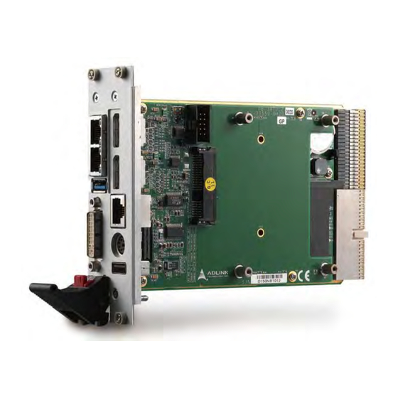
Intel® Core™ i7 processor with Mobile Intel® QM87 Express Chipset. The cPCI-3510(BL) Series is a 3U CompactPCI blade available in single-slot (4HP), dual-slot (8HP) or triple-slot (12HP) width form factors with various daughter boards to provide a broad range of I/O requirements. -
Page 14: Features
Two additional PCIe Gigabit Ethernet Controllers routed to RTM (cPCI-R3P00) Additional two Gigabit Ethernet ports on 80mm RTM (cPCI-R3P00T) Line-in and Line-out ports on faceplate (cPCI-3510(BL)D) CFast or mSATA socket for SATA interface storage Optional onboard SSD for SATA interface storage (shares space with CFast socket) 2.5"... -
Page 15: Model Number Decoder
Model Number Decoder Blades cPCI-EX 3510 D 4700E M4G / S32 (B) (C) (A) Operating Temperature Code Blank = -20°C to +70°C EX= -40°C to +85°C (for CPUs with TDP below 37W only) (B) J2 Connector Type Code 0 = HM connector 1 = UHM connector (PICMG 2.30 PlusIO compliant) - Page 16 (D) CPU Code 5700E = quad-core Intel® CoreTM i7-5700EQ processor 4700E = quad-core Intel® CoreTM i7-4700EQ processor 4402E = dual-core Intel® CoreTM i5-4402E processor (E) Memory Size Code M4 = 2x 2GB DDR3L-1600 soldered SDRAM M8 = 2x 4GB DDR3L-1600 soldered SDRAM M16 = 2x 8GB DDR3L-1333 soldered SDRAM (F) Storage Board Code Blank = Default with CFast socket...
-
Page 17: Package Contents
1.4 Package Contents The cPCI-3510(BL) is packaged with the following components. If any of the following items are missing or damaged, retain the ship- ping carton and packing material and contact the dealer for inspection. Please obtain authorization before returning any prod- uct to ADLINK. - Page 18 Blade Optional Accessories 2.5” SATA drive installation kit (P/N 58-00176-0000) Y-cable for PS/2 combo port (P/N 30-01016-2000) RJ-45 to DB-9 COM adapter cable (P/N 30-01020-0200) DisplayPort to DVI adapter cable (P/N 30-01120-0000) DisplayPort to VGA adapter cable (P/N 30-01119-0000) DisplayPort to HDMI adapter cable (P/N 30-01121-0000) USB 3.0 Type A male-to-female extension cable (P/N: 30-01175-0000) SCSI 100-pin IO cable: 2x DVI-D female, 2x DB9 male,...
-
Page 19: Specifications
• Mobile Intel® QM87 Express Chipset Memory • DDR3L-1333 SDRAM ECC soldered, up to 16GB (cPCI-3510BL) • DDR3L-1600 SDRAM ECC soldered, up to 8GB (cPCI-3510) CompactPCI • PCI 32bit/ 33MHz; 3.3V, 5V universal V(IO) • Supports operation in system slot as master or in peripheral slot... - Page 20 • Storage Temperature: -50°C to 100°C • Humidity: 95% @60°C non-condensing • Shock: 20G peak-to-peak, 11ms duration, non-operating • Vibration : 2Grms, 5-500Hz, each axis, operating (w/o hard drive) • CE EN55022 • FCC Class A Table 2-1: cPCI-3510(BL) Processor Blade Specifications Specifications...
- Page 21 • 1x 100-pin connector supports 2x DVI/DP, Line-in/Line-out, 2x USB 2.0, 2x RS-232/422/485 COM, 1x KB/MS 8HP (cPCI-3510S) • 1x USB 3.0 ports • 2x 10/100/1000BASE-T Ethernet ports • 1x DVI-I port • PMC/XMC site Table 2-1: cPCI-3510(BL) Processor Blade Specifications Specifications...
- Page 22 • PS/2 Keyboard/Mouse combo port • Line-in and Line-out port • PMC/XMC site Table 2-1: cPCI-3510(BL) Processor Blade Specifications 1. The storage device limits the operational vibration tolerance. When the application requires higher specification for anti-vibration, it is recommended to use a flash storage device.
-
Page 23: Cpci-R3P00(T) Rtm Specifications
• cPCI-R3P00: 100mm x 50mm • cPCI-R3P00T: 100mm x 80mm Dual-slot (8HP, 40.64mm) (optional single slot upon request ) Gigabit • cPCI-R3P00: Two GbE ports switched from cPCI-3510(BL) Ethernet 2x independent controller i210 • cPCI-R3P00T: Two GbE ports from independent Intel 82580DB GbE controller Serial Ports •... -
Page 24: Block Diagrams
PCIe to PCI PCIe to PCI 2x GbE 2x GbE 3x USB 3x USB Bridge Bridge ATMEL ATMEL ® ® GA128 GA128 COM4 COM4 PCI 32bit PCI 32bit IPMB 0/1 IPMB 0/1 /66MHz /66MHz Figure 2-1: cPCI-3510(BL) Blade Functional Block Diagram Specifications... - Page 25 Daughter Board USB x2 Conn. Line-in, Line-out Codec SATA0 2.5” HDD/SDD PS/2, KB/MS Figure 2-2: cPCI-3510(BL)D Daughter Board Functional Block Diagram Specifications...
- Page 26 Daughter Board Conn. DVI/DP SATA0 2.5” HDD/SSD DVI/DP COM1 COM2 10-pin KB/MS Figure 2-3: cPCI-3510(BL)G Daughter Board Functional Block Diagram Specifications...
-
Page 27: Figure 2-2: Cpci-3510(Bl)D Daughter Board Func. Block Diagram 13 Figure 2-3: Cpci-3510(Bl)G Daughter Board Func. Block Diagram 14 Figure 2-4: Cpci-3510L Daughter Board Func. Block Diagram
Daughter Board USB x1 Conn. USB x1 Horizontal Type A RS232/422/485 SATA0 2.5” HDD GbE 3 82574L GbE 4 82574L Figure 2-4: cPCI-3510L Daughter Board Functional Block Diagram Specifications... -
Page 28: Figure 2-5: Cpci-3510M Daughter Board Func. Block Diagram
cPCI-3510M Daughter Board 100-pin Conn. high Line-in, Line-out density connector 2x DVI/DP 2.5” HDD/Slim SATA0 2x USB 2.0 2x COM (RS232/422/485) KB/MS Figure 2-5: cPCI-3510M Daughter Board Functional Block Diagram Specifications... -
Page 29: Figure 2-6: Cpci-R3P00 Rtm Functional Block Diagram
RTM COM (Tx, Rx) 2x USB GbE 1/2 SATA3/4/5 7 pin 7 pin 7 pin USB3 RS232/422/485 FT2 32R Figure 2-6: cPCI-R3P00 RTM Functional Block Diagram Specifications... -
Page 30: Figure 2-7: Cpci-R3P00T Rtm Functional Block Diagram
cPCI-R3P00T RTM COM (Tx, Rx) 2x USB PC Ie x4 GbE 3/4 82580DB SATA3/4/5 7 pin 7 pin 7 pin U SB3 RS232/422/485 FT2 32R Figure 2-7: cPCI-R3P00T RTM Functional Block Diagram Specifications... -
Page 31: I/O Connectivity Table
1 (SATA) Storage 1 (CFast) 1 (CFast) 1 (CFast) 1 (CFast) Onboard optional optional optional optional Line-in Audio Line-out PMC/XM Table 2-3: cPCI-3510(BL) I/O Connectivity 1. Available by replacing CFast or mSATA socket adapter board with onboard SSD adapter board. Specifications... - Page 32 Audio Line-out Line-out PMC/XMC Table 2-3: cPCI-3510(BL) I/O Connectivity (cont’d) 1. Available by replacing CFast or mSATA socket adapter board with onboard SSD adapter board. 2. Routed from CPU blade faceplate for cPCI-R3P00; independent of CPU blade for cPCI-R3P00T (GbE controller onboard).
-
Page 33: Power Requirements
2.5 Power Requirements In order to guarantee a stable functionality of the system, it is rec- ommended to provide more power than the system requires. An industrial power supply unit should be able to provide at least twice as much power as the entire system requires of each voltage. - Page 34 Series when using the Intel® Core™ i7 processors with 4GB DDR3L-1600 ECC soldered memory and onboard 64GB SATA flash disk. The cPCI-3510(BL) is powered by 5V and 3.3V. Power consumption at 100% CPU usage was measured using the Intel Thermal Analysis Tool (TAT).
-
Page 35: Functional Description
The processor includes an Integrated Display Engine, Processor Graphics and Integrated Memory Controller. The cPCI-3510(BL) Series supports Intel® Core™ i7/i5 processors. The table below lists the general specifications and power ratings of the CPUs supported by the cPCI-3510(BL) Series. - Page 36 Supported Technologies Core™ i7- Core™ i7- Core™ i5- Core™ i5- Features 5700EQ 4700EQ I5-4400E 4402E Intel® Virtualization Technology for Directed I/O (Intel® VT-d) Intel® Virtualization Technology (Intel® VT-x) Intel® VT-x with Extended Page — — Tables (EPT) Intel® Hyper-Threading Technology Intel®...
-
Page 37: Platform Controller Hub
3.2 Platform Controller Hub The Mobile Intel® QM87 Express Chipset provides extensive I/O support. Functions and capabilities include: The QM87 PCH provides extensive I/O support, functions and capabilities including: PCI Express Base Specification, Revision 2.0 support for up to eight ports with transfers up to 5 GT/s ACPI Power Management Logic Support, Revision 4.0a... -
Page 38: Intel® Turbo Boost Technology
Hyper-Threading Technology using the BIOS for all previ- ous versions of Windows operating systems. 3.6 Trusted Platform Module The cPCI-3510(BL) is optionally equipped with an Atmel AT97SC3204 Trusted Platform Module (TPM). The TPM is a secure controller with added cryptographic functionality to provide users a secure environment in e-commerce transactions and Internet communications. -
Page 39: Battery
IC. If the data is not matched, the IC may be blocked. 3.7 Battery The cPCI-3510(BL) is equipped with a 3.0V "coin cell" lithium bat- tery for the Real Time Clock (RTC). The battery socket is equipped on the storage carrier daughter board. The lithium battery must be replaced with an identical battery or a battery type recommended by the manufacturer. - Page 40 This page intentionally left blank. Functional Description...
-
Page 41: Board Interfaces
(UHM/HM) CN4/5 Stacked SO-CDIMM socket LAN1 Dual Ethernet connectors Layer-2 daughter board DVI1 DVI connector connector Storage daughter board USB1 USB port connector cPCI-3510(BL)G daughter U2201 Pericom PI7C9X130 board connector Figure 4-1: cPCI-3510(BL) Series Board Layout (component side) Board Interfaces... -
Page 42: Figure 4-2: Cpci-3510(Bl) Series Board Layout (Solder Side)
Reset Button Figure 4-2: cPCI-3510(BL) Series Board Layout (solder side) Board Interfaces... -
Page 43: Cpci-3510(Bl) Blade Assembly Layout
4.2 cPCI-3510(BL) Blade Assembly Layout This section describes the final assembly layout of the single slot cPCI-3510(BL) Blade. Heatsink CFast CFast carrier board Figure 4-3: cPCI-3510(BL) Blade Assembly Layout Battery CFast CFast socket Clear CMOS jumper CompactPCI connector J2 (UHM/HM) Board Interfaces... -
Page 44: Cpci-3510(Bl)D Blade Assembly Layout
4.3 cPCI-3510(BL)D Blade Assembly Layout The dual-slot width cPCI-3510(BL)D Blade is comprised of the cPCI-3510 single-slot main board and the cPCI-3510(BL)D daugh- ter board to expand I/O connectivity with PS/2, COM, 2x USB ports, Line-in, and Line-out ports . COM1... -
Page 45: Cpci-3510(Bl)G Blade Assembly Layout
4.4 cPCI-3510(BL)G Blade Assembly Layout The dual-slot width cPCI-3510(BL)G Blade is comprised of the cPCI-3510 single-slot main board and the cPCI-3510(BL)G daughter board to expand I/O connectivity with PS/2, COM, USB ports, and 2x DisplayPorts. COM2 2.5” SATA HDD... -
Page 46: Cpci-3510L Blade Assembly Layout
4.5 cPCI-3510L Blade Assembly Layout The dual-slot width cPCI-3510L Blade is comprised of the cPCI-3510 single-slot main board and the cPCI-3510L daughter board, expanding I/O connectivity with 2x LAN, COM, USB. LAN1 SATA1 2.5” SATA HDD COM1 cPCI-3510L daughter board... -
Page 47: Cpci-3510M Blade Assembly Layout
4.6 cPCI-3510M Blade Assembly Layout The dual-slot width cPCI-3510M Blade is comprised of the cPCI-3510 single-slot main board and the cPCI-3510M daughter board, expanding I/O connectivity with a 100-pin high density con- nector. SATA0 cPCI-3510M daughter board 100-pin high density... -
Page 48: Cpci-3510(Bl)/D/G Faceplate
Reset Button Power LED GP LED DVI-I Thermal LED WDT LED HDD LED cPCI-3510(BL)G PS/2 DisplayPorts KB/MS COM1 USB 2.0 Reset Button Power LED DVI-I GP LED Thermal LED WDT LED HDD LED Figure 4-8: cPCI-3510(BL)/D/G Faceplate Layout Board Interfaces... -
Page 49: Cpci-3510L, Cpci-3510M Faceplate
4.8 cPCI-3510L, cPCI-3510M Faceplate cPCI-3510L LAN Connector Power LED Reset Button DVI-I GP LED Thermal LED WDT LED HDD LED cPCI-3510M 100-pin connector Power LED Reset Button DVI-I GP LED Thermal LED WDT LED HDD LED Figure 4-9: cPCI-3510L, cPCI-3510M Faceplate Layout... -
Page 50: Table 4-1: Cpci-3510(Bl) Faceplate System Led Descriptions
Yellow ON/Blinking Defined by user Table 4-1: cPCI-3510(BL) Faceplate System LED Descriptions 1. Power, WDT, Overheat, GP LEDs are connected to GPIO pins of IPMC. The Power, WDT, Thermal LEDs can be programmed by the user as general purpose LEDs. -
Page 51: Cpci-R3P00(T) Rtm Board Layout
4.9 cPCI-R3P00(T) RTM Board Layout LAN1/2 USB1 SATA2 USB10 SATA SATA VGA1 COM4 COM5* RS-232/422/485 port LAN1/2 Dual Ethernet ports (converted from USB) COM4 RS-232 port (Tx, Rx only) VGA1 VGA port SATA2/3/4 SATA ports USB1/10 USB ports CompactPCI connector... -
Page 52: Cpci-R3P00(T) Rtm Faceplate
4.10 cPCI-R3P00(T) RTM Faceplate COM4 COM5 USBx2 GbE x2 Figure 4-11: cPCI-R3P00(T) RTM Faceplate Board Interfaces... -
Page 53: Connector Pin Assignments
4.11 Connector Pin Assignments USB 2.0 Connectors Pin # Signal Name UV0- UV0+ Table 4-2: USB 2.0 Pin Definition USB 3.0 Connectors Pin # Signal Name USB3.0_P5VA USB2_CMAN USB2_CMAP USB3A_CMRXN USB3A_CMRXP USB3A_CMTXN USB3A_CMTXP Board Interfaces... -
Page 54: Table 4-3: Vga Pin Definition
DB-15 VGA Connector Signal Name Pin # Pin # Signal Name Green Blue N.C. +5V. N.C. CRTDATA HSYNC VSYNC CRTCLK Table 4-3: VGA Pin Definition DisplayPort Connectors Pin # Signal Pin # Signal CN_DP0_P Ground CN_DP0_N CN_DP1_P Ground CN_DP1_N CN_DP2_P Ground CN_DP2_N CN_DP3_P... -
Page 55: Table 4-5: Dvi-I Connector Pin Definition
DVI-I Connector Pin # Signal Pin # Signal TMDS Data2- Hot Plug Detect TMDS Data2+ TMDS Data0- TMDSData0+ DDC Clock [SCL] DDC Data [SDA] Analog vertical sync TMDS Clock + TMDS Data1- TMDS Clock - TMDS Data1+ Analog Red... -
Page 56: Table 4-6: Rj-45 Gbe Pin Definitions
RJ-45 Gigabit Ethernet Connectors 10BASE-T/ Pin # 1000BASE-T 100BASE-TX LAN_TX0+ LAN_TX0- LAN_TX1+ — LAN_TX2+ — LAN_TX2- LAN_TX1- — LAN_TX3+ — LAN_TX3- Table 4-6: RJ-45 GbE Pin Definitions Speed Activity Speed LED Activity LED Status (Green/Orange) (Yellow) Network link is not established or system powered off Link 10 Mbps... -
Page 57: Table 4-8: Ps/2 Keyboard/Mouse Pin Definition
RTS-L — — CTS-L — — RI-L — — Table 4-9: cPCI-3510(BL)D/P COM1 (DB-9) Pin Definition The COM mode setting for cPCI-3510(BL)D/P models is set using SW1~SW4. See “COM1 Mode Selection Switches (SW1~SW4)” on page 46. NOTE: NOTE: Board Interfaces... -
Page 58: Table 4-10: Cpci-3510(Bl)D/P Com1 Mode Switch Settings
COM1 Mode Selection Switches (SW1~SW4) These switches set the cPCI-3510(BL)D/P COM1 to RS-232 full modem, RS-422, RS-485, or RS-485+ half-duplex mode. Switches SW1~SW4 are located on the top edge of the cPCI-3510(BL)D daughter board. RS-232 full modem is set by default. Mode RS-232... -
Page 59: Table 4-11: Cpci-3510(Bl)G Com1 (Rj-45) Pin Definition
— — RI-L — — Table 4-11: cPCI-3510(BL)G COM1 (RJ-45) Pin Definition The COM mode settings for cPCI-3510(BL)G models are set in the BIOS: see “Output (cPCI-3510(BL)G COM1/2)” on page 104. NOTE: NOTE: COM1 Connector with DB-9 Adapter An RJ-45 to DB-9 adapter cable is provided to breakout the COM1 signals. -
Page 60: Table 4-13: Rs-422/485 Adapter Dongle Pin Definition
Table 4-13: RS-422/485 Adapter Dongle Pin Definition COM1 with RS-422/485 Dongle (DB-9) Pin # RS-422 RS-485 TXD- TXD- TXD+ TXD+ RXD+ — RXD- — — — — — — — — — — — Table 4-14: cPCI-3510(BL)G COM1 with RS-422/485 Dongle Pin Definition Board Interfaces... -
Page 61: Table 4-15: Cpci-3510(Bl)G Com2 Pin Header Definition
Ground — — — — Table 4-15: cPCI-3510(BL)G COM2 Pin Header Definition The COM mode settings for cPCI-3510(BL)G models are set in the BIOS: see “Output (cPCI-3510(BL)G COM1/2)” on page 104. NOTE: NOTE: cPCI-R3P00(T) RTM Serial Ports COM4 Connector (DB-9)) -
Page 62: Table 4-17: Cpci-R3P00(T) Com5 Pin Definition
The cPCI-R3P00(T) RTM COM5 RS-422/485 pin definitions are different from the common DB-9 pin definitions. An RS-422/485 DB-9 male-female adapter dongle allows compatibility with com- NOTE: NOTE: mon RS-422/485 pin definitions. See “RS-422/485 Adapter Don- gle for cPCI-3510(BL)G” on page 48 Pin # RS-232 RS-422 RS-485 DCD-L —... -
Page 63: Table 4-19: Cpci-3510M 100-Pin I/O Connector Pin Definition
100-pin I/O Connector (CN4) Pin # Signal Pin # Signal USB9_CN-N USB9_CN-P USB1_CN-N USB1_CN-P TMDS_I2C_DATA TMDS_I2C_CLK TMDSB_DATA2B TMDSB_DATA2 TMDSB_DATA1B TMDSB_DATA1 TMDSB_DATA0B TMDSB_DATA0 TMDSB_CLKB TMDSB_CLK P5V_DVI1 TMDSB_HPD NC TMDS_I2C_DATA TMDS_I2C_CLK TMDSB_DATA2B TMDSB_DATA2 TMDSB_DATA1B TMDSB_DATA1 TMDSB_DATA0B TMDSB_DATA0 TMDSB_CLKB TMDSB_CLK P5V_DVI2... - Page 64 Pin # Signal Pin # Signal KBCLK_CN KBDATA_CN COM1_RXD_CN COM1_CTS-L_CN COM1_TXD_CN COM1_RTS-L_CN COM1_DTR-L_CN COM1_DSR-L_CN COM1_DCD-L_CN COM2_RXD_CN COM2_CTS-L_CN COM2_TXD_CN COM2_RTS-L_CN COM2_DTR-L_CN COM2_DSR-L_CN COM2_DCD-L_CN AGND_AU AGND_AU L_IN_R L_IN_L L_IN_JD AGND_AU HP_R HP_L HP_JD AGND_AU Table 4-19: cPCI-3510M 100-pin I/O Connector Pin Definition Board Interfaces...
-
Page 65: Table 4-20: Sata Connector On Rtm
Serial ATA Connectors on RTM (CN4-R, CN5-R) Pin # Signal Table 4-20: Serial ATA Connector on RTM SATA Conn. on cPCI-3510(BL)D/(BL)G/M Daughter Board Pin # Signal Signal Power P13~P15 Table 4-21: SATA on cPCI-3510(BL)D/(BL)G/M Daughter Board Pin Def’n Board Interfaces... -
Page 66: Table 4-22: Cfast Socket Pin Definition
CFast Socket (on CFast carrier board) Pin # Signal Name Ground SATA_TX-P SATA_TX-N Ground SATA_RX-N SATA_RX-P Ground CFast_CDI Ground Ground CFast_LED1 CFast_LED2 P3V3 P3V3 Ground Ground CFast_CDO Table 4-22: CFast Socket Pin Definition Board Interfaces... -
Page 67: Table 4-23: Layer-2 Daughter Board Connector Pin Definition
Layer-2 Daughter Board Connector (CN1) Signal Name Pin # Pin # Signal Name USB2-N -12V USB2-P USB3-N HDA_SDIN0 USB3-P HDA_R_SDOUT SATA_ICH_RX-N0 HDA_R_SYNC SATA_ICH_RX-P0 HDA_R_BIT_CLK SATA_TX-P0 CK_L2_PCIE1-P SATA_TX-N0 CK_L2_PCIE1-N PCIE_TXN5 CK_L2_PCIE2-P PCIE_TXP5 CK_L2_PCIE2-N PCIE_RXN5 HDA_R_RST-L PCIE_RXP5 SPKR L2_PCIE_RST-L PCIE_RXN4 PCIE_RXP4... -
Page 68: Table 4-24: Storage Daughter Board Connector Pin Definition
Storage Daughter Board Connector (CN2) Signal Name Pin # Pin # Signal Name PCH_SPKR CLK33_TPM SIO_SPKR LPC_FRAME-L TPM_RST-L CN_VCC_RTC LPC_AD3 LPC_AD2 LPC_AD1 LPC_AD0 TPM_LPCPD PCH_SERIRQ TPM_CLKRUN TPM_GPIO SATA_PCH_RX-N0 SATA_PCH_RX-P0 SATA_PCH_TX-N0 SATA_PCH_TX-P0 CFast_CDI CFast_CDO P3V3 P3V3 Table 4-24: Storage Daughter Board Connector Pin Definition Board Interfaces... -
Page 69: Table 4-25: Cpci-3510(Bl)G Db Connector Pin Definition
COM2_RTS-L COM2_DSR-L COM2_SOUT COM2_SIN PCH_DDPD_AUXN PCH_DDPC_AUXN PCH_DDPD_AUXP PCH_DDPC_AUXP PCH_DDPD_0N PCH_DDPC_0N PCH_DDPD_0P PCH_DDPC_0P PCH_DDPD_1N PCH_DDPC_1N PCH_DDPD_1P PCH_DDPC_1P PCH_DDPD_2N PCH_DDPC_2N PCH_DDPD_2P PCH_DDPC_2P PCH_DDPD_3N PCH_DDPC_3N PCH_DDPD_3P PCH_DDPC_3P DDPD_CTRLCLK DDPC_CTRLCLK DDPD_CTRLDATA DDPC_CTRLDATA DDPD_HPD DDPC_HPD Table 4-25: cPCI-3510(BL)G Daughter Board Connector Pin Definition Board Interfaces... -
Page 70: Table 4-26: Pmc/Xmc Daughter Board Connector Pin Definition
PMC/XMC Daughter Board Connector (on cPCI-3510(BL)D/(BL)G daughter board) Signal Name Pin # Pin # Signal Name -12V +12V CK_PCIE1_P CK_PCIE1_N PCIE_TXN2 CK_PCIE2_P PCIE_TXP2 CK_PCIE2_N PCIE_R_RXN2 PCIE_R_RXP2 PCIE_RST# PCIE_R_RXN1 PCIE_R_RXP1 PCIE_TXN4 PCIE_TXP4 +3.3V +3.3V Table 4-26: PMC/XMC Daughter Board Connector Pin Definition... -
Page 71: Table 4-27: Pmc Connector Pin Definitions
PMC Connector on PMC/XMC Daughter Board (JN1/2) Pin# JN1 Signal JN2 Signal PMC_TCK P12V N12V PMC_TRST-L PMC_TMS PCIX_INTA-L NC (PMC_TDO) PCIX_INTB-L PMC_TDI PCIX_INTC-L PMC_MOD-L1 PCIX_INTD-L PMC_MOD-L2 P3V3_PMCAUX P3V3 CLK66_PCIX_PMC PMC_RST-L PMC_MOD-L3 P3V3 PCIX_GNT-L0 PMC_MOD-L4 PCIX_REQ-L0 PMC_PME-L PMC_VIO PCIX_AD30 PCIX_AD31... - Page 72 Pin# JN1 Signal JN2 Signal PCIX_FRAME-L PCIX_TRDY-L PCIX_IRDY-L P3V3 PCIX_DEVSEL-L PCIX_STOP-L PCIX_PCIXCAP PCIX_PERR-L PCIX_LOCK-L P3V3 PCIX_SERR-L PCIX_PAR PCIX_CBE-L1 PMC_VIO PCIX_AD14 PCIX_AD15 PCIX_AD13 PCIX_AD12 PCIX_M66EN PCIX_AD11 PCIX_AD10 PCIX_AD9 PCIX_AD8 P3V3 PCIX_AD7 PCIX_CBE-L0 PCIX_AD6 P3V3 PCIX_AD5 PCIX_AD4 PMC_VIO PCIX_AD3 PCIX_AD2 PCIX_AD1 PCIX_AD0 PCIX_ACK64-L P3V3 PCIX_REQ64-L...
-
Page 73: Table 4-28: Xmc Connector Pin Definition
XMC Connector on PMC/XMC Daughter Board (JN3) Pin# 3.3V VPWR Not used PCIE_RST-L 3.3V VPWR Not used Not used 3.3V VPWR Not used +12V 3.3V VPWR Not used -12V Not used VPWR Not used Not used VPWR Not used 3.3V... -
Page 74: Table 4-29: Compactpci J1 Connector Pin Definition
CompactPCI J1 Connector REQ64# ENUM# +3.3V CPCI_AD1 CPCI_VIO CPCI_AD0 ACK64# +3.3V CPCI_AD4 CPCI_AD3 CPCI_AD2 CPCI_AD7 +3.3V CPCI_AD6 CPCI_AD5 +3.3V CPCI_AD9 CPCI_AD8 CPCI_M66EN CPCI_CBE-L0 GND CPCI_AD12 CPCI_AD11 CPCI_AD10 +3.3V CPCI_AD15 CPCI_AD14 CPCI_AD13 GND CPCI_SERR-L +3.3V CPCI_PAR CPCI_CBE-L1 GND +3.3V CPCI_PERR-L GND GND CPCI_DEVSEL-L CPCI_PCIXCAP CPCI_STOP-L CPCI_LOCK-L GND +3.3V... -
Page 75: Table 4-30: Compactpci J2 Connector Pin Definition
CompactPCI J2 Connector PCI_CLK6 LAN2_TXDP1 LAN1_TXDP3 LAN1_TXDP1 PCI_CLK5 LAN2_TXDN1 LAN1_TXDN3 LAN1_TXDN1 GND LAN2_TXDP0 LAN1_TXDP2 LAN1_TXDP0 LAN2_TXDP3 LAN2_TXDP2 LAN2_TXDN0 LAN1_TXDN2 LAN1_TXDN0 GND LAN2_TXDN3 LAN2_TXDN2 J2_RSTJ CPCI_REQ_L6 CPCI_GNT_L6 GND GND CLK_PCIE8_N CLK_PCIE6_P DEGJ GND CLK_PCIE8_P CLK_PCIE6_N FALJ CPCI_REQ_L5 CPCI_GNT_L5 GND 3PE_CLK-... -
Page 76: Table 4-31: Cpci-R3P00 Rj2 Connector Pin Definition
cPCI-R3P00 rJ2 Connector Pin Z 22 GND 21 GND 2_ETH_B+ 1_ETH_D+ 1_ETH_B+ 20 GND 2_ETH_B- 1_ETH_D- 1_ETH_B- 19 GND 2_ETH_A+ 1_ETH_C+ 1_ETH_A+ 18 GND 2_ETH_D+ 2_ETH_C+ 2_ETH_A- 1_ETH_C- 1_ETH_A- 17 GND 2_ETH_D- 2_ETH_C- 16 GND 15 GND 14 GND DDC_DAT 13 GND VGA_HSY DDC_CLK... -
Page 77: Table 4-32: Cpci-R3P00T Rj2 Connector Pin Definition
Connector Pin Z 22 GND 21 GND 20 GND 19 GND 18 GND 17 GND 16 GND 4PE_CLK- 2_PE_CLK+ 15 GND 4PE_CLK+ 2_PE_CLK- 14 GND 3PE_CLK+ 1_PE_CLK+ 4_PE_CLKE# DDC_DAT 13 GND 3PE_CLK- 1_PE_CLK- 3_PE_CLKE# VGA_HSY DDC_CLK 12 GND... -
Page 78: Jumper Settings
4.12 Jumper Settings Load BIOS Default Jumper (JP1) The cPCI-3510(BL) Load BIOS Default Jumper is located on the CF/CFast storage board. To load the default BIOS settings, short pins 2-3 on JP1, then reinstall the jumper cap to pins 1-2. -
Page 79: Getting Started
PCI Mezzanine Card Processor blade installation to chassis RTM installation to chassis 5.1 CPU and Heatsink The cPCI-3510(BL) Series come with CPU and heatsink pre-installed. Removal of heatsink/CPU by users is not recom- mended. Please contact your ADLINK service representative for assistance. -
Page 80: Sata Drive Installation
5.2 SATA Drive Installation The cPCI-3510(BL)D/(BL)G/P/L/M 2/3-slot versions provide space to install a slim type 2.5" Serial-ATA storage drive. SATA Drive Installing a - cPCI-3510(BL)D/(BL)G/P/L/M 1. A 2.5" SATA drive can be assembled in the location marked as below. 2. 2.Prepare a 2.5" SATA drive and locate the brackets and screws in the accessory kit. - Page 81 3. Screw the brackets to the 2.5" SATA drive. 4. Align the drive assembly with the cPCI-3510(BL) and insert it into the onboard SATA connector until it is prop- erly seated. Getting Started...
- Page 82 5. Secure the hard drive assembly to the cPCI-3510(BL) with four M2.5 screws provided. Getting Started...
-
Page 83: Installing A Cfast Card
5.3 Installing a CFast Card To install a CFast card, locate the CFast connector on the CFAST storage board and insert the card until it is properly seated. Getting Started... -
Page 84: Installing The Cpci-3510(Bl) To The Chassis
5.4 Installing the cPCI-3510(BL) to the Chassis The cPCI-3510(BL) may be installed in a system or peripheral slot of a 3U CompactPCI chassis. These instructions are for reference only. Refer to the user guide that comes with the chassis for more information. -
Page 85: Rtm Installation - Cpci-R3P00(T)
RTMs. Refer to previous sections for peripheral connectivity of all I/O ports on the RTM. When installing the cPCI-3510(BL) Series and related RTMs, make sure the RTM is the correct matching model. - Page 86 This page intentionally left blank. Getting Started...
-
Page 87: Driver Installation
Driver Installation The cPCI-3510(BL) drivers are available from the ADLINK website (http://www.adlinktech.com/PD/web/PD_detail.php?cKind=& pid=1291). ADLINK provides validated drivers for Windows 7 64-bit. We recommend using these drivers to ensure compatibility. The VxWorks BSP can be downloaded from the cPCI-3510(BL) product page on the ADLINK website 6.1 cPCI-3510(BL) Drivers... -
Page 88: Ethernet Controller Driver
6.2 Ethernet Controller Driver 1. Extract the contents of …\LAN\Intel® I210 Gigabit Net- work connection_Win7 64bit_12.7.28.0.zip. 2. Open the Device Manager and go to Other Devices. You will see a "question mark" next to Ethernet Controller R-click on Ethernet Controller and choose "Update Driver Software…". Driver Installation... - Page 89 3. Click “Browse my computer for driver software”. 4. Navigate to the folder where you extracted the contents of the zip file and click “OK”. Click “Next” to install the driver. Driver Installation...
-
Page 90: Usb-To-Serial Converter Driver (Rtm)
USB3 port by a USB-to-serial converter (see " cPCI-R3P00 RTM” on page 17). To install the driver for the converter, follow the pro- cedure below. 1. Extract the contents of …\cPCI-3510\COM\CDM 2.08.28 WHQL Certified-x64.zip. 2. Open the Device Manager and go to Other Devices. You will see a "question mark"... - Page 91 3. Click “Browse my computer for driver software”. 4. Navigate to the folder where you extracted the contents of the zip file and click “OK”. Click “Next” to install the driver Driver Installation...
- Page 92 This page intentionally left blank. Driver Installation...
-
Page 93: Watchdog Timer
This section describes the operation of the cPCI-3510’s watchdog timer (WDT). The primary function of the WDT is to monitor the cPCI-3510's operation and to reset the system if a software appli- cation fails to function as programmed. The following WDT func-... - Page 94 Reset Watchdog Timer This command is used to reload the WDT. Action Byte Value Description NetFn/LUN Request Defined command Response Complete Code 00h means OK Set Watchdog Timer This command is used to start and restart the Watchdog Timer using the specified countdown value. Action Byte Value...
- Page 95 Action Byte Value Description Pre-timeout interval in Request 1h~ffh ( ‘1h’ based.) seconds. [7] - reserved [6] - reserved [5] - OEM [4] - SMS/OS [3] - OS Load Timer Use Expiration flags [2] - BIOS/POST clear [1] - BIOS FRB2...
- Page 96 Action Byte Value Description [7] - reserved [6:4] - pre-timeout interrupt 000b = none 001b = SMI (optional) 010b = NMI / Diagnostic Interrupt (optional) 011b = Messaging Interrupt 100b,111b = reserved Timer Actions [3] - reserved [2:0] - timeout action 000b = no action 001b = Hard Reset 010b = Power Down...
-
Page 97: Figure 7-1: Example Procedure For Configuring The Wdt
Example WDT Programming Procedure Configuration of the watchdog timer is via serial interface. A detailed description of the WDT IPMI commands can be found above. The following example shows the procedure for configuring the WDT works over a serial console. See “Communications with IPMC”... - Page 98 2. Reload the WDT counter by using the raw IPMI command "Reset Watchdog Timer". "Reset Watchdog Timer" Command: [18 00 22] Successful response to Command: [1C 00 22 00] 3. Get the WDT configuration by using the "Get Watchdog Timer" command. "Get Watchdog Timer"...
-
Page 99: Bios Setup Utility
BIOS Setup Utility The following chapter describes basic navigation for the AMI EFI BIOS setup utility. 8.1 Starting the BIOS To enter the setup screen, follow these steps: 1. Power on the motherboard 2. Press the < Delete > key on your keyboard when you see the following text prompt: <... - Page 100 Setup Menu The main BIOS setup menu is the first screen that you can navi- gate. Each main BIOS setup menu option is described in this user’s guide. The Main BIOS setup menu screen has two main frames. The left frame displays all the options that can be configured.
- Page 101 There is a hot key legend located in the right frame on most setup screens. NOTE: NOTE: The < F8 > key on your keyboard is the Fail-Safe key. It is not dis- played on the key legend by default. To set the Fail-Safe settings of the BIOS, press the <...
- Page 102 The < F2 > key on your keyboard is the previous values key. It is not displayed on the key legend by default. To set the previous values settings of the BIOS, press the < F2 > key on your keyboard. It is located on the upper row of a stan- dard 101 keyboard.
- Page 103 The < F4 > key allows you to save any changes you have made and exit Setup. Press the < F10 > key to save your changes. The following screen will appear: Press the < Enter > key to save the configuration and exit.
-
Page 104: Main Setup
8.2 Main Setup When you first enter the Setup Utility, you will enter the Main setup screen. You can always return to the Main setup screen by select- ing the Main tab. There are two Main Setup options. They are described in this section. -
Page 105: Advanced Bios Setup
8.3 Advanced BIOS Setup Select the Advanced tab from the setup screen to enter the Advanced BIOS Setup screen. You can select any of the items in the left frame of the screen, such as SuperIO Configuration, to go to the sub menu for that item. -
Page 106: Acpi Settings
8.3.1 ACPI Settings You can use this screen to select options for the ACPI Advanced Configuration Settings. Use the up and down < Arrow > keys to select an item. Use the < + > and < - > keys to change the value of the selected option. -
Page 107: Trusted Computing
8.3.2 Trusted Computing Trusted Computing is an industry standard to make personal com- puters more secure through a dedicated hardware chip, called a Trusted Platform Module (TPM). This option allows you to enable or disable the TPM support. Security Device Support OS will not show TPM. -
Page 108: Cpu Configuration
8.3.3 CPU Configuration You can use this screen to select options for the CPU Configura- tion Settings. Use the up and down < Arrow > keys to select an item. Use the < + > and < - > keys to change the value of the selected option. -
Page 109: Sata Configuration
EIST Set this value to Enabled/Disabled. Turbo Mode Set this value to Enabled/Disabled. 8.3.4 SATA Configuration You can use this screen to select options for the SATA Configura- tion Settings. An example of the SATA Configuration screen is shown below. -
Page 110: Pch-Fw Configuration
SATA Port 0~4 Display SATA device name string. Set this value to Enabled/Dis- abled. Hot Plug Appears when SATA mode is AHCI. SATA port Hot Plug support. Set this value to Enabled/Disabled. 8.3.5 PCH-FW Configuration Intel TXT(LT) Configuration You can use this screen to view ME related information. For exam- ple, ME FW Version, ME Firmware Mode, ME Firmware Type, ME Firmware SKU..etc. -
Page 111: Intel ® Anti-Theft Technology Configuration
8.3.6 Intel ® Anti-Theft Technology Configuration You can use this screen to select options for the Intel AT Configu- ration Settings. An example of the Intel AT Configuration screen is shown below. Intel® Anti-Theft Support Set this value is Enable/Disable. -
Page 112: Amt Configuration
8.3.7 AMT Configuration You can use this screen to select options for the AMT settings. Use the up and down < Arrow > keys to select an item. Use the < + > and < - > keys to change the value of the selected option. Intel AMT Intel AMT feature. -
Page 113: Usb Configuration
8.3.8 USB Configuration You can use this screen to select options for the USB Configura- tion. Use the up and down < Arrow > keys to select an item. The screen is shown below. Legacy USB Support Enables legacy USB support. Auto option disables legacy support if no USB devices are connected. -
Page 114: Hardware Monitor
8.3.9 Hardware Monitor This option displays the current status of all of the monitored hard- ware devices/components such as voltages and temperatures. CPU Temperature Displays current CPU temperature. System Temperature Displays current system temperature. 3.3V Displays current system 3.3V voltage. Displays current system 5V voltage. -
Page 115: 10Super Io Configuration
8.3.10 Super IO Configuration You can use this screen to select options for the Super IO Config- uration settings. Serial Port 1,2,3,4 Configuration Set Parameters of Serial Port 1,2,3,4 (COM 1,2,3,4). COM1/2: faceplate; COM3: IPMI interface; COM4: RTM. Serial Port Enable/Disable serial port 1,2,3,4 (COM1,2,3,4). - Page 116 Set the mode of serial port 1,2,(COM1,2). Set this value to RS232 or RS422/RS485. The cPCI-3510(BL)G COM1/2 Output BIOS setting is only used for cPCI-3510(BL)G models. The COM mode setting for cPCI-3510(BL)D/P models must be set using the “COM1 Mode NOTE: NOTE: Selection Switches (SW1~SW4)”...
-
Page 117: 11Console Redirection
8.3.11 Console Redirection You can use this screen to select options for the serial port con- sole redirection settings. An example of the Serial Port Console Redirection screen is shown below. Console Redirection Set this value to Enabled/Disabled. Console Redirection Settings The settings specify how the host computer and the remote com- puter will exchange data. - Page 118 Terminal Type VT100+ is the preferred terminal type for out-of-band manage- ment. Configuration options: VT100, VT100+, VT-UTF8, ANSI. Bits per second Select the bits per second you want the serial port to use for console redirection. The options are 115200, 57600, 38400, 19200, 9600.
- Page 119 Stop Bits Stop bits indicate the end of a serial data packet. (A start bit indicates the beginning). The standard setting is 1 stop bit. Communication with slow devices may require more than 1 stop bit. Set this value to 1 and 2.
-
Page 120: Chipset Setup
8.4 Chipset Setup Select the Chipset tab from the setup screen to enter the Chipset BIOS Setup screen. You can select any of Chipset BIOS Setup options by highlighting it using the < Arrow > keys. The Chipset BIOS Setup screen is shown below. BIOS Setup Utility... -
Page 121: Pch-Io Configuration
8.4.1 PCH-IO Configuration PCH LAN Controller Enable or disable onchip NIC. Set this value to Enabled/Disabled HD Audio Enable or disable the onboard HDA controller. Set this value to Enabled/Disabled. BIOS Setup Utility... - Page 122 PCI Express Configuration PCI Express Clock Gating Enable or disable XHCI Pre-Boot Driver support. Set this value to Enabled/Disabled. DMI Link ASPM Control Mode of operation of xHCI controller. Set this value to Enabled/Disabled. Subtractive Decode Mode of operation of xHCI controller. Set this value to Enabled/Disabled.
- Page 123 USB Configuration XHCI Pre-Boot Driver Enable or disable XHCI Pre-Boot Driver support. Set this value to Enabled/Disabled. XHCI Mode Mode of operation of xHCI controller. Set this value to Enabled/Disabled. HS Port #1/2/3/4 Switchable Allows for HS port switching between xHCI and EHCI. If dis- abled, port is routed to EHCI.
-
Page 124: System Agent (Sa) Configuration
EHCI1/2 Control the USB EHCI (USB 2.0) functions. One EHCI control- ler must always be enabled. Set this value to Enabled/Dis- abled. USB Ports Per-Port Disable Control Control the per-port disabling of USB ports 0~13. Set this value to Enabled/Disabled. 8.4.2 System Agent (SA) Configuration VT-d... - Page 125 Graphics Configuration Primary Display Select which graphics device should be the primary display. Set this value to Auto, IGFX, PCI. Internal Graphics Keep IGD enabled based on the setup options. Set this value to Auto, Enabled, Disabled. GTT Size Select the GTT size.
- Page 126 DVMT Pre-Allocated Select DVMT 5.0 Pre-Allocated (fixed) graphics memory size used by the internal graphics device. Configuration options as below: DVMT Total Gfx Memory Select DVMT 5.0 total graphic memory size used by the inter- nal graphics device. Configuration options as below: BIOS Setup Utility...
- Page 127 Memory Configuration Memory Remap Enable or disable memory remap above 4G. Set this value to Enabled/Disabled. BIOS Setup Utility...
-
Page 128: Boot Settings
8.5 Boot Settings Select the Boot tab from the setup screen to enter the Boot BIOS Setup screen. You can select any of the items in the left frame of the screen, such as Boot Device Priority, to go to the sub menu for that item. -
Page 129: Csm Parameter
Set Boot Priority Set Boot Option #1 ~2 boot priority. Hard Disk Drive BBS Priorities Specifies the boot device priority sequence from available hard drives. 8.5.1 CSM Parameter OpROM execution, boot option filter, etc. Launch CSM This option controls if CSM will be launched. Set this value to Always, Never. - Page 130 Launch Video OpROM policy This option controls the execution of UEFI and Legacy Video OpROM. Set this value to Do not launch, UEFI only, Legacy only. Other PCI device ROM priority For PCI devices other than Network, Mass storage or Video defines which OpROM to launch.
-
Page 131: Security Setup
8.6 Security Setup Administrator, User Password If only the administrator's password is set, then this only limits access to setup and is only asked for when entering setup. If only the user's password is set, then this is a power on password and must be entered to boot or enter setup. -
Page 132: Save & Exit Menu
8.7 Save & Exit Menu Select the Save & Exit tab from the setup screen to enter the Save & Exit BIOS Setup screen. You can display an Exit BIOS Setup option by highlighting it using the < Arrow > keys. The Save & Exit BIOS Setup screen is shown below. - Page 133 Discard Changes and Reset Reset system setup without saving any changes. Save Changes Save changes done so far to any of the setup options. Discard Changes Discard changes done so far to any of the setup options. Restore Changes Restore/Load Defaults values for all the setup options.
- Page 134 Save as User Defaults Save the changes done so far as user defaults.. Restore User Defaults Save changes done so far to any of the setup options. This page intentionally left blank. BIOS Setup Utility...
-
Page 135: Ipmi User Guide
IPMI User Guide 9.1 Introduction This chapter is written for those who already have a basic under- standing of the newest implementation of the baseboard manage- ment controller (BMC) of the Intelligent Platform Management Interface (IPMI) specification rev. 1.5. It also describes the OEM extension IPMI command usages which are not listed in the IPMI specification. - Page 136 IPMI IPM Controller Req Command NetFn Spec (PICMG 2.9) Platform Event (a.k.a. 23.3 Optional “Event Message”) Sensor Device Commands Get Device SDR Info 29.2 Optional Get Device SDR 29.3 Optional Reserve Device SDR 29.4 Optional Repository Set Sensor Hysteresis 29.6 Optional Get Sensor Hysteresis 29.7...
-
Page 137: Oem Commands Summary Table
9.3 OEM Commands Summary Table Command NetFn Code Cmd Code OemShowRevision OEM (C0h) OemRescanGaInput OEM (C0h) OemTestFunction OEM (C0h) OemReportGeoAddress OEM (C0h) OemEnableSmbus OEM (C0h) OemDisableSmbus OEM (C0h) OemDispDebugVariable OEM (C0h) OemResetHost OEM (C0h) OemPowerOff OEM (C0h) OemPowerOn OEM (C0h) - Page 138 OemRescanGaInput This command is used to rescan the geo-address input pins and reset the IPMB address according to the input value. Action Byte Value Description NetFn/LUN for OEM Request OEM defined command Complete Code 00h means OK Response New IPMB address New IPMB address value OemTestFunction Internal test purposes only.
- Page 139 OemDisableSmbus This command is used to shut down I2C bus access. Action Byte Value Description NetFn/LUN for OEM Request OEM defined command Response Complete Code 00h means OK OemDispDebugVariable This command can report up to 5 interval values for debug pur- poses.
-
Page 140: Compactpci Address Map
OemPowerOff This command is implemented to control the system’s status if power-off is required. Operators can control the system remotely. Action Byte Value Description NetFn/LUN for OEM Request OEM defined command Response Complete Code 00h means OK OemPowerOn This command is implemented to control the system’s status if power-on is required. -
Page 141: Communications With Ipmc
CompactPCI Peripheral Address Mapping Geo. Addr. IPMB Addr. Geo. Addr. IPMB Addr. Disabled 9.5 Communications with IPMC Operating systems need to use a serial port to communicate with the IPMC. The resource setting of the serial port must be IO: 0x2E0 and IRQ:7. -
Page 142: Relevant Documents
Normal Sensor Number Sensor name Remark Reading P_CPU_VDD 1.5 V P1V8_BG 1.8 V P1V5_SSB 1.5 V P1V1_SSB 1.1 V 9.7 Relevant Documents Document Title Revision Source Intelligent Platform Document Revision 1.1 Intel Corp. Management Interface February 20, 2002 http://www.intel.com/design/ Specification v1.5 servers/ipmi/license_ipmi.htm PICMG 2.9 D1.0 January 21, 2000... -
Page 143: Important Safety Instructions
Important Safety Instructions For user safety, please read and follow all instructions, WARNINGS, CAUTIONS, and NOTES marked in this manual and on the associated equipment before handling/operating the equipment. Read these safety instructions carefully. Keep this user’s manual for future reference. - Page 144 Never attempt to fix the equipment. Equipment should only be serviced by qualified personnel. A Lithium-type battery may be provided for uninterrupted, backup or emergency power. Risk of explosion if battery is replaced with one of an incorrect type. Dispose of used batteries appropriately. WARNING: Equipment must be serviced by authorized technicians when:...
-
Page 145: Getting Service
San Jose, CA 95138, USA Tel: +1-408-360-0200 Toll Free: +1-800-966-5200 (USA only) Fax: +1-408-360-0222 Email: info@adlinktech.com ADLINK Technology (China) Co., Ltd. Address: (201203) 300 Fang Chun Rd., Zhangjiang Hi-Tech Park Pudong New Area, Shanghai, 201203 China Tel: +86-21-5132-8988 Fax: +86-21-5132-3588 Email: market@adlinktech.com... - Page 146 84 Genting Lane #07-02A, Cityneon Design Centre Singapore 349584 Tel: +65-6844-2261 Fax: +65-6844-2263 Email: singapore@adlinktech.com ADLINK Technology Singapore Pte. Ltd. (Indian Liaison Office) Address: #50-56, First Floor, Spearhead Towers Margosa Main Road (between 16th/17th Cross) Malleswaram, Bangalore - 560 055, India Tel: +91-80-65605817, +91-80-42246107 Fax:...
Need help?
Do you have a question about the cPCI-3510 and is the answer not in the manual?
Questions and answers