
Related Manuals for ADLINK Technology cPCI-6811AA


Summary of Contents for ADLINK Technology cPCI-6811AA
- Page 1 RCC/ServerWorks Champion LE-Based 6U CompactPCI Motherboard User’s Guide Recycled Paper This datasheet has been downloaded from http://www.digchip.com at this page...
- Page 3 No part of this manual may be reproduced by any mechanical, electronic, or other means in any form without prior written permission of the manufacturer. Trademarks NuIPC is a registered trademark of ADLINK Technology Inc; MS-DOS & Windows 95/NT/2000/XP registered...
- Page 4 Getting Service from ADLINK Customer Satisfaction is the most important priority for ADLINK Tech Inc. If you need any help or service, please contact us. ADLINK Technology Inc. Web Site http://www.adlinktech.com Sales & Service Service@adlinktech.com NuDAQ + USBDAQ + PXI nudaq@adlinktech.com...
-
Page 5: Table Of Contents
1.4.1 cPCI-6811AA Specifications..........12 1.4.2 cPCI-R6820 RTM Specifications ........15 1.4.3 Common Spec. for cPCI-6811AA and RTM ....... 15 1.5 Model Variations ................19 Chapter 2 Jumpers and Connectors ............ 21 2.1 cPCI-6811AA Board Outline and Illustratoin ........22 2.1.1 cPCI-6811AA Top and Front View ........ - Page 6 IDE Setting Jumper on the RTM......... 36 2.3.17 GbE Connection Selection ..........36 2.3.18 Setting Jumper on cPCI-6811AA........37 Chapter 3 Getting Started ..............39 3.1 CPU and Heatsink ................39 3.2 Memory Module Installation .............. 40 3.3 HDD Installation on Main Board............41 3.4 HDD Installation on RTM ..............
- Page 7 List of Tables Table 1: I/O Connectivity .............. 18 Table 2: CPCI-6811AA Model Table..........19 Table 3: Recommended PMC Modules ........19 Table 4: Recommended Chasses..........20 Table 5: cPCI-6811AA Table ............23 Table 6: Keyboard and Mouse Combo Connector......25 Table 7: COM1 on front board or COM2 on the RTM ....
-
Page 9: Chapter 1 Introduction
(GbE) controller on the 66MHz 64bit PCI bus. The dual GbE connections can be routed to the rear I/O connector or to a PICMG 2.16 compliant backplane. Enhanced Features The cPCI-6811AA 6U Compact PCI CPU Card adds full control functions over the cPCI-6810. The newly added “full control” allows software controllable hot-swapping. - Page 10 (Or’d with L_STAT of HB6) Swap LED Powers down board. Add one pull-high on IPMI_PWRON# GPIO7 (If the PM (Or’d with cPCI_BDSEL) doesn’t boot, the board won’t power on) HEALTHY#_OUT Healthy signal output (Or’d with on-board that leads to the cPCI healthy#_out) Reflects the system PWR_GOOD...
-
Page 11: Checklist
Checklist The cPCI-6811AA series products support both front and rear panel I/O. 1.1.1 cPCI-6811AA Front Board The cPCI-6811AA CPU module may be equipped with different capacities of RAM, HDD, and PCM depending on requirements. Please check your configurations with your dealer and check that your package is complete and contains the items below. -
Page 12: Features
Features 1.2.1 cPCI-6811AA Features • PICMG 2.16 CompactPCI Packet Switching Backplane (cPSB) Compliant • PICMG 2.9 System Management Bus Compliant • Standard 6U form factor, 1-slot (4HP) wide • Design for Intel® Pentium® III processor-Low Power running at FSB 133MHz •... -
Page 13: Functional Block
Functional Block Figure 1. cPCI-6811AA Block Diagram Introduction • 5... -
Page 14: Compactpci Bus Interface
System Slot supporting a host, or as a Non Transparent bridge in a Peripheral Slot as an intelligent subsystem. These options allow the cPCI-6811AA board to be inserted into both the Peripheral Slot and the System Slot. -
Page 15: Bios
1.3.3 BIOS The cPCI-6811AA adopts the Award BIOS with a 4-Mbit flash ROM implemented to load the BIOS. A boot block device is used to allow recovery of the BIOS in the event of a catastrophic failure (power fail during BIOS update). -
Page 16: Processor
SDRAM. The DRAM interface supports 64Mbit, 128Mbit, and 256Mbit technology, allowing up to 512Mbytes per double-sided SO-DIMM. The cPCI-6811AA can support up to 1GB of SDRAM memory with two 144-pin SO-DIMMs. . 8 • Introduction... -
Page 17: Interrupts
1.3.6 Interrupts Two enhanced interrupt controllers provide the cPCI-6811AA with a total of 15 interrupt inputs. Interrupt controller features include support for: • Level-triggered and edge-triggered inputs • Individual input masking • Fixed and rotating priorities Interrupt sources include: •... -
Page 18: Baseboard Management
1.3.10 Power Ramp Circuitry The cPCI-6811AA features a power controller with power ramp circuitry to allow the board's voltages to be ramped in a controlled fashion. The power ramp circuitry eliminates any large voltage or current spikes caused by hot swapping boards. -
Page 19: Ethernet Interfaces
1.3.13 IDE Interface The fast IDE interface on cPCI-6811AA supports up to four IDE devices including hard disk drives and CD ROMs. Each IDE device can have independent timing. The IDE interface supports PIO IDE transfers of up to 14MB/s and the Bus Master IDE up to 100MB/s. -
Page 20: Keyboard/Mouse Controller
1.3.16 Keyboard/Mouse Controller Two 6-pin circular DIN connectors are located on the front panel of single-processor version of cPCI-6811AA, for example cPCI-6811AA, for keyboard and mouse connections. The power provided to the keyboard and mouse is protected by a poly-switch rated at 1.1A. The keyboard and mouse... - Page 21 • CPU, memory operating frequency auto-detection • Bootable from USB storage devices including USB-Floppy, USB-ZIP USB-CD-ROM, and USB-HDD. • Option OEM BIOS features Customized OEM splash image / power on screen Serial remote-console redirected to serial COM1 port Due to BIOS segment limitations, enabling the remote console Note: function may occupy the same memory space as other ROM mapping add-on or boot-up devices such like Pre-boot Agent of...
- Page 22 • PS2 keyboard and mouse connector: • W82782D built-in monitoring CPU temperatures, FAN speed, system temperature, V core, and DC voltages. • Watchdog timer: Programmable I/O port 10h - 12h of bank 3 to configure watchdog timer, programmable 8-bit timer 1-255 minutes. •...
-
Page 23: Cpci-R6820 Rtm Specifications
Secondary IDE supported on one 40-pin IDE connector, one 44-pin connector for 2.5 inches HDD or flash drive; and one CompactFlash type-II socket. 1.4.3 Common Spec. for cPCI-6811AA and RTM Flash Storage Support Options: • DiskOnModule via the 40-pin IDE on RTM, 16-256MB •... - Page 24 Environment • Operating temperature: 0 - 50 °C (Note 1) • Storage temperature: -20 - 80 °C • Humidity: 5% - 95% non-condensed • Shock: 15G peak-to-peak, 11ms duration, 3 axes, 3 times/axis non-operation • Vibration: (Note 3) None-operation: 1.88Grms, 5-500Hz, 3 axes, with package Operation: 0.5Grms, 5-500Hz, each axis with flash disk drive Safety Certificate and Test •...
- Page 25 Power Requirement (Typical) Typical Current and +3.3V +12V -12V Maximum Current (+/-5%) (+/-5%) (+/-5%) (+/-5%) 2.50A 4.10A cPCI-6811AA/P10/M1G 3.88A 14.636A cPCI-6811AA/P10/M1G 1.44A 3.64A (Without PMC, VGA 3.73A 14.636A cards & RTM) cPCI-6811AA/P10/M1G 3.16A 4.76A with HDD 3.88A+HDD 14.636A Test conditions •...
-
Page 26: Table 1: I/O Connectivity
I/O Connectivity cPCI-6811AA RTM (cPCI-R6820) Faceplate Board J3/J5 Faceplate Board Serial Port (COM1) RJ-45 10-pin Serial Port (COM2) Header PS2 Keyboard PS2 Mouse DB-15 USB (port 0, port 1) USB x 2 USB (port 2, port 3) USB x 2 Gigabit Ethernet Port 1 2.16... -
Page 27: Model Variations
Model Variations The cPCI-6811AA series products include the following 4 base configurations. All models have the CPU pre-mounted. The number of SO-DIMM sockets and PMC slots are varied depending on the model. If a HDD is installed on board, it may occupy and sacrifice one PMC socket space. Note that the RTM is sold separately and are not listed in the following table. -
Page 28: Table 4: Recommended Chasses
The following table lists the recommended chassis available from ADLINK, which are compatible with the cPCI-6811AA series SBC. Chassis Description/Configuration cPCIS-6130R 19” 1U high standard depth chassis with RIO cPCIS-6400X 19” 4U high chassis, 4-slot I/O, 64-bit BP, ATX Power 19”... -
Page 29: Chapter 2 Jumpers And Connectors
Jumpers and Connectors This chapter will familiarize the user with the cPCI-6811AA before getting started; it will provide information about the board layout, connector definitions, and jumper setup. This includes the following information: • cPCI-6811AA board outline and illustration •... -
Page 30: Cpci-6811Aa Board Outline And Illustratoin
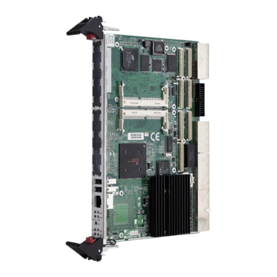
Board Outline and Illustratoin 2.1.1 cPCI-6811AA Top and Front View PMC Slot #1 SO-DIMM 3,4 SO-DIMM 1,2 PMC Slot #2 BATTERY COM 1 LED’s CPU 0 Figure 2. Top and Front View of cPCI-6811AA 22 • Jumpers and Connectors... -
Page 31: Table 5: Cpci-6811Aa Table
Single SODIMM Max. Memory 1.0 GB HDD Installation Possible PMC slot # (without HDD) PMC slot # (with HDD) Table 5: cPCI-6811AA Table Note: If a HDD is installed, then PMC slot #1 becomes unavailable. Jumpers and Connectors • 23... -
Page 32: Cpci-R6820 Board Outline And Illustratoin
cPCI-R6820 Board Outline and Illustratoin 2.2.1 cPCI-R6820 Top and Front View Secondary IDE on CF Socket COM 2 CompactPCI rJ5 USB 2 USB 3 GbE #1 40-pin Primary ID 44-pin Secondary ID GbE #2 40-pin Secondary ID KB/MS CompactPCI rJ3 2.5 inches Drive bay Figure 3. -
Page 33: Connectors Pin Assignment
Connectors Pin Assignment 2.3.1 Keyboard and Mouse Combo Connector Pin # Signal Function KBDATA Keyboard Data MSDATA Mouse Data Ground Power KBCLK Keyboard Clock MSCLK Mouse Clock Table 6: Keyboard and Mouse Combo Connector Keyboard and Mouse Combo Connector is available on the Note: cPCI-R6820 RTM only. -
Page 34: Vga Connector
RI: Ring Indicate No Connect Table 8: COM1 on the RTM 2.3.3 VGA Connector Signal Name Pin # Pin # Signal Name Green Blue N.C. +5V. N.C. N.C. HSYNC VSYNC Table 9: VGA Connector on RTM (only available for the series with VGA chip on front board) 2.3.4 USB Connector... -
Page 35: General Purpose Led Definitions
2.3.6 General Purpose LED definitions Color Status Description IDE Media IDE idle Access IDE access System is not power-on or Power OK power failed Green Power ON Board inserted and power on Hot swappable Blue status Board inserted but not power on yet. -
Page 36: 44-Pin Ide Port
2.3.8 44-pin IDE Port Signal Pin # Pin # Signal RESET- Ground DD10 DD11 DD12 DD13 DD14 DD15 Ground N.C (key pin) DMARQ Ground DIOW- Ground DIOR- Ground IORDY CSEL DMACK- Ground INTRQ reserved PDIAG- CS0- CS1- DASP- Ground Ground TYPE- Table 14: 44-pin IDE connector Primary IDE is on the front board (CN8) and the Secondary IDE is... -
Page 37: 40-Pin Ide Port
2.3.9 40-pin IDE Port Signal Pin # Pin # Signal RESET- Ground DD10 DD11 DD12 DD13 DD14 DD15 Ground +5V (for DOM) DMARQ Ground DIOW- Ground DIOR- Ground IORDY CSEL DMACK- Ground INTRQ reserved PDIAG- CS0- CS1- DASP- Ground Table 15: 40-pin Primary and Secondary IDE channels on the RTM 2.3.10 IPMB Interface on RTM Pin # Signal Name... -
Page 38: Compactpci J1 Pin Assignments
2.3.11 CompactPCI J1 Pin Assignments REQ64# ENUM# +3.3V AD [1] V (I/O) AD [0] ACK64# +3.3V AD [4] AD [3] AD [2] AD [7] +3.3V AD [6] AD [5] +3.3V AD [9] AD [8] M66EN C/BE [0]# GND AD [12] V (I/O) AD [11] AD [10]... -
Page 39: Compactpci J2 Pin Assignments
2.3.12 CompactPCI J2 Pin Assignments CLK6 BRSV BRSV BRSV CLK5 BRSV BRSV IPMBSDA IPMBSCL IPMBALR BRSV BRSV BRSV BRSV BRSV PRST# REQ6# GNT6# BRSV BRSV DEG# BRSV BRSV FAL# REQ5# GNT5# AD [35] AD [34] AD [33] AD [32] AD [38] V (I/O) AD [37] AD [36]... -
Page 40: Compactpci J3 And Rj3 Pin Assignments
2.3.13 CompactPCI J3 and rJ3 Pin Assignments +12V -12V GND LPa_DA0+ LPa_DA0- LPa_DC0+ LPa_DC0- GND LPa_DB0+ LPa_DB0- LPa_DD0+ LPa_DD0- GND LPb_DA1+ LPb_DA1- LPb_DC1+ LPb_DC1- GND LPb_DB1+ LPb_DB1- LPb_DD1+ LPb_DD1- +3.3V +3.3V +3.3V PMCIO5 PMCIO4 PMCIO3 PMCIO2 PMCIO1 PMCIO10 PMCIO9 PMCIO8 PMCIO7 PMCIO6 PMCIO15... -
Page 41: Compactpci J5 And Rj5 Pin Assignments
2.3.14 CompactPCI J5 and rJ5 Pin Assignments CS3- DASP- DIOW- DMACK- DIOR- PDIAG- DD15 INTRQ DMARQ IORDY DD12 DD13 DD14 DD10 DD11 DRESET- USB-0+ USB-0- USB-1+ USB-1- SMUX SMUX SMUX SMUX SMUX SMUX SMUX SMUX +3.3V +3.3V DDCCLK DDCDAT VSYNC HSYNC BLUE GREEN... -
Page 42: Pmc Connector Pin Assignments
2.3.15 PMC Connector Pin Assignments PMC J11/J21 and J12/J22 Connector Pin Assignments Signal Signal Signal Signal Name Name Name Name Pin # Pin # Pin # Pin # -12V +12V TRST# INTA# INTB# INTC# INTD# +3.3V +3.3V CLKP1 RST# GNT0# +3.3V REQ0# PME#... - Page 43 PMC J13/J23 and J24 Connector Pin Assignments Signal Signal Signal Signal Name Name Name Pin # Pin # Name Pin # Pin # PMCIO1 PMCIO2 CBE [7] PMCIO3 PMCIO4 CBE [6] CBE [6] PMCIO5 PMCIO6 CBE [5] PMCIO7 PMCIO8 PAR64 PMCIO9 PMCIO10 AD63...
-
Page 44: Ide Setting Jumper On The Rtm
2.3.16 IDE Setting Jumper on the RTM A CompactFlash (CF) socket is available on the RTM as a Secondary IDE port. A 3-pin jumper (CN12) is used to set the CF card as either master or slave device of the IDE channel. 3 2 1 CF card is a Master IDE device 3 2 1... -
Page 45: Setting Jumper On Cpci-6811Aa
A 3-pin jumper (JP1) is used to set the SBC as either “in normal operation” or “forcing the SBC to SYSTEM mode”. Note: When cPCI-6811AA is in the Packet Switching Backplane has no PCI bus, please set JP1 as “1-2”. -
Page 47: Chapter 3 Getting Started
• Main board installation CPU and Heatsink The cPCI-6811AA SBC supports the Intel® Pentium® processor – Low Voltage, which is pre-mounted to the PCB (printed circuit board). The heatsink is also pre-mounted in the factory. There are no jumper settings necessary to set the CPU operating frequency or CPU type. -
Page 48: Memory Module Installation
Memory Module Installation The cPCI-6811AA SBC supports up to two sockets of 144-pin PC-133 registered ECC SO-DIMM’s. The maximum memory capacity is 1GB. If memory modules are pre-installed when you receive the your package, this section can be skipped. The chipset supports 64Mb, 128Mb, 256Mb, and 512Mb memory technologies. -
Page 49: Hdd Installation On Main Board
HDD Installation on Main Board A slim-type 2.5-inch HDD can be mounted to the cPCI-6811AA main board. If a HDD is pre-installed when you receive the cPCI-R6820 product package, this section maybe skipped. Step 1: Remove the PMC Key-bolt of the PMC slot #1. -
Page 50: Pci Mezzanine Card (Pmc) Installation
This section describes important information regarding the use of the rear I/O connections. Refer to section 2.4 for peripheral connectivity of all I/O ports on the RTM. When installing the cPCI-6811AA and its RTM, make sure the RTM is the correct model that matches its front board. -
Page 51: Main Board Installation
Main Board Installation Use the following procedure to install the cPCI-6811AA main board to its CompatPCI chassis. Step 1: Refer to the relevant chassis user manual for pre-preparation of the chassis before installing the main board. Users need to assign a slot to the board. Be sure to select the correct slot (system or peripheral) depending the operation purpose of the board. -
Page 53: Chapter 4 Device Driver Installation
Device Driver Installation To install the drivers for the cPCI-8611, refer to the installation information in this chapter. Basic information is presented in this section, however, for more detailed installation information for non-Windows Operating Systems, refer to the extensive explanation inside the ADLINK CD. The drivers are located in the following directories of the CD-ROM: LAN driver \CHIPDRV\LAN\82546EB\win2kxp... -
Page 54: Lan Drivers Installation
LAN Drivers Installation This chapter describes the LAN driver installation for the onboard Ethernet controller Intel 82546EB. All associated drivers are located under the following ADLINK CD directory: X:\CHIPDRV\LAN\82546EB, where X: is the location of the CD-ROM drive. 4.1.1 Software and Drivers Support The 82546EB driver supports the following OS or platforms: •... -
Page 55: Appendix A Ipmi Functions List
IPMI Functions List The following table lists the IPMI V1.0 functions that are supported by the cPCI-6811AA. IPMI V1.0 Function List CPCI-6811AA IPM Device “Global” Commands Get Device ID √ Cold Reset √ Warm Reset √ Get Self Test Results √... - Page 56 Platform Event (a.k.a. “Event Message”) √ PEF and Alerting Commands Sensor Device Commands Get Device SDR Info √ Get Device SDR √ Reserve Device SDR Repository √ Get Sensor Reading Factors √ Set Sensor Hysteresis Get Sensor Hysteresis √ Set Sensor Threshold Get Sensor Threshold √...
-
Page 57: Ipmi Address Map
SEL Device Commands Get SEL Info √(1) Get SEL Allocation Info √(1) Reserve SEL √(1) Get SEL Entry √(1) Add SEL Entry √(1) Partial Add SEL Entry √(1) Delete SEL Entry Clear SEL √(1) Get SEL Time √(1) Set SEL Time √(1) (1) Supported on PCB rev.A3 or higher. -
Page 59: Appendix B Watchdog Timer Programming Guide
WatchDog Timer Programming Guide The Watchdog Timer (WDT) can monitor the system’s status. Once a value is given to the WDT, the timer will begin to count down. If the system idles or hangs, the system will reboot itself when the timer times out. The Watch Dog timer includes an 8-bit timer clocked by a 1-minute internal clock that is derived from the battery-backed 32.768KHz crystal clock generator. -
Page 60: Wdt Setup Procedures
WDT Setup Procedures Followings are the Watch Dog Timer setup procedures: Set pin 55 of PC87417 as Watch Dog Timer output pin Set Bit 7 of SIOCF2 Register (Index: 22H) to 1, for example: • o 2E 22 • o 2F 80 Set Logic Device to System Wake-Up Control (SWC) Set Logic Device Number Register (Index: 07H) to 04H, for example: •... - Page 61 Select Bank 3 for Watch Dog Timer from SWC base address. Set Bit 1-0 of BANKSEL Register (I/O Base: 840H, Offset: 0FH) to 11, for example: • o 84F 03 Set the count down value for Watch Dog timer. Set count down value to WDTO Register (I/O Base: 840H, Offset: 11H) 00000000: Reserved 00000001: 1 minute...
-
Page 63: Appendix C Smbus Address Map
SMBus Address Map The SMBus address Map on cPCI-6820 products are as following. Address (Hex) Function Device 0x A0 SO-DIMM ID SO-DIMM 0x 5C Hardware Monitor ADM1026 0x AC SEL data storage (IPMI) 24C64 0x AE FRU data storage (IPMI) 24C64 0x AA BIOS CMOS storage... -
Page 65: Warranty Policy
Warranty Policy Thank you for choosing ADLINK. To understand your rights and enjoy all the after-sales services we offer, please read the following carefully. Before using ADLINK’s products please read the user manual and follow the instructions exactly. When sending in damaged products for repair, please attach an RMA application form which can be downloaded from: http://rma.adlinktech.com/policy/. - Page 66 • Damage caused by inappropriate storage environments such as with high temperatures, high humidity, or volatile chemicals. • Damage caused by leakage of battery fluid during or after change of batteries by customer/user. • Damage from improper repair by unauthorized ADLINK technicians.
Need help?
Do you have a question about the cPCI-6811AA and is the answer not in the manual?
Questions and answers