
Subscribe to Our Youtube Channel
Related Manuals for ADLINK Technology cPCI-9116


Summary of Contents for ADLINK Technology cPCI-9116
- Page 1 64-ch, 16-bit, 250KS/s Analog Input Card for 3U CompactPCI User’s Manual Manual Rev.: July 7, 2020 Revision Date: 50-15002-1020 Part No: Leading EDGE COMPUTING...
- Page 2 Leading EDGE COMPUTING Revision History Revision Release Date Description of Change(s) 1.10 2003-04-28 Initial release Update to current specification and 2020-07-07 software support.
- Page 3 Preface Copyright © 2020 ADLINK Technology Inc. This document contains proprietary information protected by copy- right. All rights are reserved. No part of this manual may be repro- duced by any mechanical, electronic, or other means in any form without prior written permission of the manufacturer.
- Page 4 Leading EDGE COMPUTING California Proposition 65 Warning WARNING: This product can expose you to chemicals including acrylamide, arsenic, benzene, cadmium, Tris(1,3-dichloro-2-propyl) phosphate (TDCPP), 1,4- Dioxane, formaldehyde, lead, DEHP, styrene, DINP, BBP, PVC, and vinyl materials, which are known to the State of California to cause cancer, and acrylamide, benzene, cadmium, lead, mercury, phthalates, toluene, DEHP, DIDP, DnHP, DBP, BBP, PVC, and vinyl materials, which are known to the State of California to cause...
-
Page 5: Table Of Contents
MAPS/LV, LabVIEW Support ........7 1.4.3 MAPS/C, C & C++ Support ........8 2 Installation ................9 What You Have..............9 Unpacking................10 cPCI-9116 Layout .............. 11 PCI Configuration .............. 12 2.4.1 Plug and Play ............12 2.4.2 Configuration ............12 2.4.3... - Page 6 Leading EDGE COMPUTING 3.1.2 J1 Connector Legend ..........15 Analog Input Signal Connection......... 15 3.2.1 Types of Signal Sources........... 16 3.2.2 Input Configurations..........16 Digital I/O Connection ............18 4 Operation Theory ............. 19 A/D Conversion Procedure ..........19 4.1.1 Conversion in Software Polling Mode.......
-
Page 7: List Of Figures
Figure 1-2: ADLINK Connection Explorer (ACE) ......6 Figure 1-3: ACE Soft Front Panel ..........7 Figure 2-1: PCB Layout of the cPCI-9116 ........11 Figure 3-1: J1 Pin Assignments ..........14 Figure 3-2: Single-ended Mode and Floating sources ....16 Figure 3-3: Ground-referenced source and differential input .. - Page 8 Leading EDGE COMPUTING This page intentionally left blank. viii List of Figures...
-
Page 9: List Of Tables
List of Tables Table 3-1: J1 Connector Legend ............ 15 List of Tables... - Page 10 Leading EDGE COMPUTING This page intentionally left blank. List of Tables...
-
Page 11: Introduction
Introduction The cPCI-9116 series products are advanced data acquisition cards based on the 32-bit CompactPCI architecture. The cPCI- 9116 series includes: cPCI-9116: 16-bit 250KHz DAS card for 3U CompactPCI The cPCI-9116 series DAS cards use state-of-the-art technology making them ideal for data logging and signal analysis applica- tions in the medical and process control industries. -
Page 12: Applications
Leading EDGE COMPUTING 1.2 Applications Automotive testing Cable testing Transient signal measurement Laboratory automation Biotech measurement 1.3 Specifications 1.3.1 Analog Input Converter: LT1606 (or equivalent) 250KHz Number of channels: (programmable) 64 single-ended (SE) 32 differential input (DI) Mixing of SE and DI analog signal between channels allowed A/D Data FIFO buffer size: 1024 locations Channel gain queue length: 512-word configurations Resolution: 16-bit... - Page 13 Accuracy Input Range Accuracy ±5, 0 to 10V 0.01% of FSR ±2.5, 0 to 5V 0.02% of FSR ±1.25, 0 to 2.5V 0.02% of FSR ±0.625, 0 to 1.25V 0.04% of FSR Input Impedance: 100 MΩ | 6pF Time-base Source:...
-
Page 14: Digital I/O (Dio)
Leading EDGE COMPUTING 1.3.2 Digital I/O (DIO) Channels: 8 TTL compatible digital inputs and outputs Input Voltage: Low: VIL = 0.8 V max. IIL = 0.2mA max. High: VIH = 2.0V max. IIH = 0.02mA max. Output Voltage: Low: VOL = 0.5 V max. IOL = 8mA max. High: VOH = 2.7V min.;... -
Page 15: Software Support
1.4 Software Support ADLINK provides versatile software drivers and packages to suit various user approaches to building a system. Aside from pro- gramming libraries, such as DLLs, for most Windows-based sys- tems, ADLINK also provides drivers for other application environments such as LabVIEW. -
Page 16: Maps Core
Leading EDGE COMPUTING 1.4.1 MAPS Core ADLINK MAPS Core is a software package that includes all the device drivers for Windows and a system level management tool called ACE (ADLINK Connection Explorer). With MAPS Core installed, the operating system can identify ADLINK's devices cor- rectly and assign the necessary resources for low-level access, such as IO read/write or direct memory access. -
Page 17: Maps/Lv, Labview Support
ADLINK Connection Explorer (ACE) also provides a ready-to-use soft-front panel for digitizer products. By clicking the Launch but- ton in the lowest "Utility" block, this soft-front panel allows users to control digitizers through the UI and display the acquired wave- form/data on the screen. -
Page 18: Maps/C, C & C++ Support
Leading EDGE COMPUTING 1.4.3 MAPS/C, C & C++ Support For customers who develop their own programs in C or C++ envi- ronments, install the MAPS/C software package. MAPS/C includes all the software components required for developing applications in C/C++, such as header files, a device API library and versatile sample programs for understanding how to manipu- late the device correctly. -
Page 19: Installation
Installation This chapter describes how to install the cPCI-9116 series cards. The contents of the package and unpacking information that you should be aware of are described first. The cPCI-9116 series cards perform an automatic configuration of the IRQ, port address, and BIOS address. You do not need to set these configurations as you would in ISA form factor DAS cards. -
Page 20: Unpacking
Do not install or apply power to equipment that is damaged or missing components. Retain the shipping carton and packing materials for inspection. Please contact your ADLINK dealer/ WARNING: vendor immediately for assistance and obtain authorization before returning any product. You are now ready to install your cPCI-9116. Installation... -
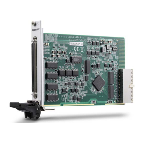
Page 21: Cpci-9116 Layout
2.3 cPCI-9116 Layout Figure 2-1: PCB Layout of the cPCI-9116 Installation... -
Page 22: Pci Configuration
Leading EDGE COMPUTING 2.4 PCI Configuration 2.4.1 Plug and Play As a plug and play component, the board requests an interrupt number via a system call. The system BIOS responds with an interrupt assignment based on the board information and on known system parameters. -
Page 23: Signal Connections
3.1 Connectors and Pin Assignment The cPCI-9116 is equipped with one 100-pin SCSI-type connector (J1). J1 is used for digital input/output, analog input, and timer/counter signals. The pin assignment for the connector is illustrated in Figure 3-1. -
Page 24: 100-Pin Scsi-Type Connector (J1)
Leading EDGE COMPUTING 3.1.1 100-pin SCSI-type Connector (J1) U_CMMD AGND AIH0 AI32 AIL0 AIH1 AI33 AIL1 AIH2 AI34 AIL2 AIH3 AI35 AIL3 AIH4 AI36 AIL4 AIH5 AI37 AIL5 AIH6 AI38 AIL6 AIH7 AI39 AIL7 AIH8 AI40 AIL8 AIH9 AI41 AIL9 AIH10 AI10 AI42... -
Page 25: J1 Connector Legend
Table 3-1: J1 Connector Legend 3.2 Analog Input Signal Connection The cPCI-9116 series provides up to 64 single-ended or 32 differ- ential analog input channels. You can set and fill the channel gain queue to get the desired combination of the input signal types. The analog signals can be converted to digital values by the A/D con- verter. -
Page 26: Types Of Signal Sources
Single-ended Mode In single-ended mode, all input signals are connected to ground provided by the cPCI-9116 card. It is suitable for connections with floating signal sources. Figure 3-2 illustrates single-ended connec- tion. Note that when more than two floating sources are con- nected, these sources will be referenced to the same common ground. -
Page 27: Figure 3-3: Ground-Referenced Source And Differential Input
Figure 3-3: Ground-referenced source and differential input Figure 3-4 shows how to connect a floating signal source to the cPCI-9116 card in differential input mode. For floating signal sources, a resistor is required on each channel to provide a bias return path. -
Page 28: Digital I/O Connection
Figure 3-5: Ground-referenced source & U_CMMD connections 3.3 Digital I/O Connection The cPCI-9116 series card provides 8 digital input and 8 digital output channels. The digital I/O signals are fully TTL/DTL compat- ible. The details of the digital I/O signal specification can be found in section 1.3.2. -
Page 29: Operation Theory
Operation Theory The operation theory of the functions on the cPCI-9116 series is described in this chapter. The functions include the A/D conver- sion, Digital I/O and General Purpose Counter / Timer. The opera- tion theory can help you better understand how to configure and program the cPCI-9116 series card. -
Page 30: Channel Gain Queue Configuration
Leading EDGE COMPUTING the data is ready. The A/D data is now ready to be transferred to host memory from the FIFO. This method is suitable for applications that need to process AD data in real time. Under this mode, the timing of the A/D conver- sion is fully controlled by the software. -
Page 31: Programmable Scan Acquisition Mode
4.2 Programmable Scan Acquisition Mode 4.2.1 Scan Timing and Procedure It's recommended that this mode be used if your application needs a fixed and precise A/D sampling rate. You can accurately pro- gram the period between conversions of each individual channel in the scan and the period between conversions of the entire scan. -
Page 32: Figure 4-1: Scan Timing
Leading EDGE COMPUTING 3 scans, 4 samples per scan (SC_Counter = 3, DIV_Counter = 4) ( channel sequences are specified in Channel Gain Queue) Scan_start AD_conversion Scan_in_progress )(pin47) Acquisition_in_progress Sampling Interval t= Scan Interval T= SI2_COUNTER/TimeBase SI_COUNTER/TimeBase Figure 4-1: Scan Timing In scan acquisition mode, the channel, gain, and input configura- tions (single-end, differential, or U_CMMD) must be specified in the hardware Channel Gain Queue. -
Page 33: Channel Gain Queue Configuration
Scan with SSH You can send the SSH_OUT signal on pin 47 of J1 to external S&H circuits to sample and hold all signals if you want to simulta- neously sample all channels in a scan, as illustrated in Figure 4-1. -
Page 34: Trigger Modes
Leading EDGE COMPUTING 4.2.3 Trigger Modes There are five trigger modes (software-trigger, pre-trigger, post- trigger, middle-trigger, and delay-trigger) to start the data acquisi- tion described in Scan Timing and Procedure. All but software trig- ger are external digital triggers. An external digital trigger event occurs when a rising edge or a falling edge (software programma- ble) of a digital signal is detected on pin 46 of J1. -
Page 35: Figure 4-2: Pre-Trigger (Trigger Occurs After M Scans)
(M_counter = M = 3, DIV_counter = 4, SC_counter = 0) ExtTrg(pin46) Scan_start AD_conversion Scan_in_progress )(pin47) Acquisition_in_progress Aquired data Acquired & stored data (M scans) Operation start Figure 4-2: Pre-trigger (trigger occurs after M scans) If an external trigger event occurs when a scan is in progress, the data acquisition won’t stop until this scan completes, and... -
Page 36: Figure 4-4: Pre-Trigger With M_Enable = 0 (Before M Scans)
Leading EDGE COMPUTING When an external trigger signal occurs before the first M scans of data are converted, the amount of stored data could be fewer than the originally specified amount of DIV_counter * M_counter, as illustrated in Figure 4-4. This situation can be avoided by setting M_enable. -
Page 37: Figure 4-5: Pre-Trigger With M_Enable = 1
(M_counter = M = 3, DIV_counter = 4, SC_counter = 0) The first M scans Trigger signals which occur in the shadow region(the first M scans) will be ignored ExtTrg(pin46) Scan_start AD_conversion Scan_in_progress )(pin47) Acquisition_in_progress Aquired data Acquired & stored data... -
Page 38: Figure 4-6: Middle Trigger With M_Enable = 1
Leading EDGE COMPUTING However, if M_enable is set to 0, the trigger signal will be accepted at any time. Figure 4-6 shows the acquisition timing with M_enable = 1. (M_Counter = M = 3, DIV_Counter = 4, SC_Counter = N = 1) The first M scans Trigger signals which occur in the shadow region(the first M scans) will be ignored... -
Page 39: Figure 4-7: Middle Trigger (Trigger With Scan Is In Progress)
If an external trigger event occurs when a scan is in progress, the stored N scans of data would include this scan. The first stored data will always be the first channel entry of a scan, as illus- trated in Figure 4-7. -
Page 40: Figure 4-8: Post Trigger
Leading EDGE COMPUTING Post-Trigger Acquisition Use post-trigger acquisition in applications where you want to col- lect data after an external trigger event. The number of scans after the trigger is specified in SC_counter, as illustrated in Figure 4-8. The total acquired data length = DIV_counter * SC_counter. (DIV_Counter = 4, SC_Counter = 3) ExtTrg Scan_start... -
Page 41: Figure 4-9: Delay Trigger
(24MHz) or A/D sampling clock (Timebase/ SI2_counter). When the count reaches 0, the counter stops and the cPCI-9116 card starts to acquire data. The total acquired data length = DIV_counter * SC_counter. (DIV_Counter = 4, SC_Counter = 3) -
Page 42: Figure 4-10: Post Trigger With Re-Trigger
Leading EDGE COMPUTING Post-Trigger or Delay-trigger Acquisition with Re-trigger Use post-trigger or delay-trigger acquisition with re-trigger function in applications where you want to collect data after several exter- nal trigger events. The number of scans after each trigger is spec- ified in SC_counter, and users can program Retrig_no to specify the number of re-triggers. -
Page 43: A/D Data Transfer Modes
4.3 A/D Data Transfer Modes After the end of the A/D conversion, A/D data are buffered into the Data FIFO memory. The FIFO size on the cPCI-9116 series card is 1024 (1K) words. If the sampling rate is 10 KHz, the FIFO can buffer 102.4 ms of analog signal. -
Page 44: Digital Input And Output
Leading EDGE COMPUTING when it becomes the master on the bus. Bus mastering reduces the size of the onboard memory and reduces the CPU loading because data is directly transferred to the computer’s memory without host CPU intervention. Bus-mastering DMA provides the fastest data transfer rates on the PCI-bus. -
Page 45: General Purpose Timer/Counter Operation
4.5 General Purpose Timer/Counter Operation An independent 16-bit up/down timer/counter is designed in the FPGA for user applications. Figure 4-11 shows a simplified model of the timer/counter on the cPCI-9116 series card. It has the fol- lowing features: CPCI-9116 Controller... -
Page 46: Figure 4-12: Mode 0 Operation
Leading EDGE COMPUTING Mode 0: Interrupt on Terminal Count Mode 0 is typically used for event counting, as illustrated in Figure 4-12. After the initial count is written, OUT is initially low, and will remain low until the counter counts to zero. OUT then goes high and will remain high until a new count is written into the counter. -
Page 47: Important Safety Instructions
Important Safety Instructions For user safety, please read and follow all instructions, Warnings, Cautions, and Notes marked in this manual and on the associated device before handling/operating the device, to avoid injury or damage. S'il vous plaît prêter attention stricte à tous les avertissements et mises en garde figurant sur l'appareil , pour éviter des blessures... - Page 48 Never attempt to repair the device, which should only be serviced by qualified technical personnel using suitable tools A Lithium-type battery may be provided for uninterrupted backup or emergency power. Risk of explosion if battery is replaced with one of an incorrect type;...
- Page 49 BURN HAZARD Touching this surface could result in bodily injury. To reduce risk, allow the surface to cool before touching. RISQUE DE BRÛLURES Ne touchez pas cette surface, cela pourrait entraîner des blessures. Pour éviter tout danger, laissez la surface refroidir avant de la toucher.
-
Page 50: Getting Service
San Jose, CA 95138, USA Tel: +1-408-360-0200 Toll Free: +1-800-966-5200 (USA only) Fax: +1-408-360-0222 Email: info@adlinktech.com ADLINK Technology (China) Co., Ltd. 300 Fang Chun Rd., Zhangjiang Hi-Tech Park Pudong New Area, Shanghai, 201203 China Tel: +86-21-5132-8988 Fax: +86-21-5132-3588 Email: market@adlinktech.com ADLINK Technology GmbH Hans-Thoma-Straße 11...
Need help?
Do you have a question about the cPCI-9116 and is the answer not in the manual?
Questions and answers