
Related Manuals for ZiLOG eZ80F92


Summary of Contents for ZiLOG eZ80F92
- Page 1 Development Kit User Manual PRELIMINARY UM013904-0203 ZiLOG Worldwide Headquarters • 532 Race Street • San Jose, CA 95126 Telephone: 408.558.8500 • Fax: 408.558.8300 • www.ZiLOG.com...
- Page 2 Document Disclaimer ZiLOG is a registered trademark of ZiLOG Inc. in the United States and in other countries. All other products and/or service names mentioned herein may be trademarks of the companies with which they are associated. ©2003 by ZiLOG, Inc. All rights reserved. Information in this publication concerning the devices, applications, or technology described is intended to suggest possible uses and may be superseded.
-
Page 3: Safeguards
Development Kit User Manual Safeguards The following precautions must be observed when working with the devices described in this document. Caution: Always use a grounding strap to prevent damage resulting from electrostatic discharge (ESD). UM013904-0203 PRELIMINARY Safeguards... - Page 4 Development Kit User Manual PRELIMINARY UM013904-0203...
-
Page 5: Table Of Contents
Flash Module ........ - Page 6 Development Platform ......59 eZ80F92 Flash Module ........64 Appendix A.
-
Page 7: List Of Figures
Development Platform Block Diagram with eZ80F92 Flash Module ......4 ® Figure 2. - Page 8 Figure 25. Schematic Diagram, #4 of 9—NOR Flash Device ..67 Figure 26. Schematic Diagram, #5 of 9—eZ80F92 Flash Module . . . 68 Figure 27. Schematic Diagram, #6 of 9—IrDA Reset ... . 69 Figure 28.
- Page 9 Development Kit User Manual List of Tables ® Table 1. eZ80 Development Platform Hardware Specifications . . 2 ® Table 2. eZ80 Development Platform Peripheral Bus Connector Identification—JP1 ......12 ®...
- Page 10 Development Kit User Manual List of Tables PRELIMINARY UM013904-0203...
-
Page 11: Introduction
LEDs, including a 7x5 LED matrix – Platform configuration jumpers 1. Other members of the eZ80Acclaim! product line include the eZ80F91 and eZ80F93 microcon- trollers. A scaled-down eZ80F92 Ethernet Module is also available. Contact your local ZiLOG Sales Office for more information. -
Page 12: Hardware Specifications
– 512KB off-chip SRAM – Real-Time Clock with Battery Back-Up • ZPAKII Debug Interface • eZ80F92 Development Kit Software and Documentation CD-ROM Hardware Specifications ® Table 1 lists the specifications of the eZ80 Development Platform. ® Table 1. eZ80 Development Platform Hardware Specifications Operating Temperature: 20ºC ±5ºC... -
Page 13: Ez80 Development Platform Overview
Flash Module, can operate in stand-alone mode with Flash memory, or interface via the ZPAKII emulator to a host PC running ZiLOG Devel- oper Studio II Integrated Development Environment (ZDS IDE) software. The address bus, data bus, and all eZ80F92 Flash Module control signals ® are buffered on the eZ80 Development Platform to provide sufficient... -
Page 14: Figure 1. Ez80 ® Development Platform Block Diagram With
Development Kit User Manual ® A block diagram of the eZ80 Development Platform and the eZ80F92 Flash Module is shown in Figure 1. Peripheral Device Signals Peripheral Device Signals eZ80F92 Address Bus Address Bus eZ80™ Flash MPU Module Data Bus... - Page 15 figure. Note: Key to blocks A–E. A. Power and serial communications. D. Application module interfaces. B. eZ80F92 Flash Module interface. E. GPIO and LED with Address Decoder. C. Debug interface. ®...
-
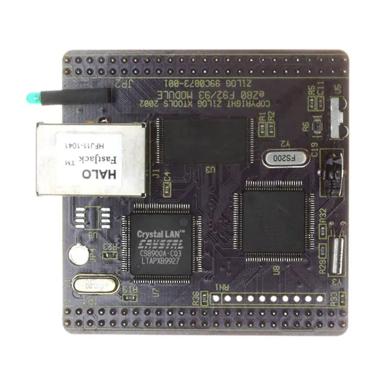
Page 16: Figure 3. The Ez80F92 Flash Module
Development Kit User Manual Figure 3 is a photographic representation of the eZ80F92 Flash Module segmented into its key blocks, as shown in the legend for the figure. Note: Key to blocks A–C. A. eZ80F92 Flash Module interfaces. B. CPU. -
Page 17: Ez80 ® Development Platform
® The eZ80 Development Platform consists of seven major hardware blocks. These blocks, listed below, are diagrammed in Figure 4. • eZ80F92 Flash Module interface (2 female headers) • ® Power supply for the eZ80 Development Platform, the eZ80F92 Flash Module, and application modules •... -
Page 18: Figure 4. Basic Ez80
Development Kit User Manual Peripheral Device Signals Address Bus eZ80™ Flash MPU Module Data Bus Interface RS232-0 (Console) SRAM (512 KB RS485 up to 2 MB) RS232-1 (Modem) Embedded Modem (7x5 matrix) Push- buttons GPIO EEPROM Address Decoder Register Application Module Headers ®... -
Page 19: Physical Dimensions
Development Kit User Manual Physical Dimensions ® The dimensions of the eZ80 Development Platform PCB is 177.8mm x182.9mm. The overall height is 38.1mm. See Figure 5. 175.3 mm 43.2 mm 114.3 mm 96.5 mm 55.9 mm 157.5 mm 167.6 mm 5.1 mm... -
Page 20: Operational Description
Development Platform. The purpose of the eZ80 Development Platform is to provide the application developer with a tool to evaluate the features of the eZ80F92 Flash MCU, and to develop an application without build- ing additional hardware. eZ80F92 Flash Module Interface The eZ80F92 Flash Module interface provides easy connection of the ®... -
Page 21: Figure 6. Ez80 ® Development Platform Peripheral Bus Connector Pin Configuration-Jp1
Development Kit User Manual V3.3_EXT GND_EXT A1 6 GND_EXT DIS_FLASH DIS_ETH V3.3_EXT GND_EXT MREQ IOREQ GND_EXT INSTRD BUSACK BUSREQ HEADER 25X2 IDC50 ® Figure 6. eZ80 Development Platform Peripheral Bus Connector Pin Configuration—JP1 UM013904-0203 PRELIMINARY Operational Description... -
Page 22: Table 2. Ez80 ® Development Platform Peripheral Bus Connector Identification-Jp1
The entire interface is represented in the eZ80F92 Module Schematics on pages 62 through 2. The Power and Ground nets are connected directly to the eZ80F92 device. 3. External capacitive loads on RD, WR, IORQ, MREQ, D0–D7 and A0–A23 should be below 10pF ®... - Page 23 The entire interface is represented in the eZ80F92 Module Schematics on pages 62 through 2. The Power and Ground nets are connected directly to the eZ80F92 device. 3. External capacitive loads on RD, WR, IORQ, MREQ, D0–D7 and A0–A23 should be below 10pF ®...
- Page 24 The entire interface is represented in the eZ80F92 Module Schematics on pages 62 through 2. The Power and Ground nets are connected directly to the eZ80F92 device. 3. External capacitive loads on RD, WR, IORQ, MREQ, D0–D7 and A0–A23 should be below 10pF ®...
- Page 25 The entire interface is represented in the eZ80F92 Module Schematics on pages 62 through 2. The Power and Ground nets are connected directly to the eZ80F92 device. 3. External capacitive loads on RD, WR, IORQ, MREQ, D0–D7 and A0–A23 should be below 10pF ®...
-
Page 26: Figure 7. Ez80 ® Development Platform I/O Connector Pin Configuration-Jp2
Development Kit User Manual I/O Connector Figure 7 illustrates the pin layout of the I/O Connector in the 50-pin ® header, located at position JP2 on the eZ80 Development Platform. Table 3 describes the pins and their functions. GND_EXT... -
Page 27: Table 3. Ez80 ® Development Platform I/O Connector Identification-Jp2
1. For the sake of simplicity in describing the interface, Power and Ground nets are omitted from this table. The entire interface is represented in the eZ80F92 Module Schematics on pages 62 through 2. The Power and Ground nets are connected directly to the eZ80F92 device. UM013904-0203 PRELIMINARY Operational Description... - Page 28 1. For the sake of simplicity in describing the interface, Power and Ground nets are omitted from this table. The entire interface is represented in the eZ80F92 Module Schematics on pages 62 through 2. The Power and Ground nets are connected directly to the eZ80F92 device. Operational Description PRELIMINARY UM013904-0203...
- Page 29 62 through 2. The Power and Ground nets are connected directly to the eZ80F92 device. Almost all of the connectors’ signals are received directly from the CPU. Three input signals, in particular, offer options to the application devel- oper by disabling certain functions of the eZ80F92 Flash Module.
-
Page 30: Application Module Interface
RS232 or the RS485 interfaces on the eZ80 Devel- opment Platform. Note: *These inputs are only used if external Flash is present on the eZ80F92 Flash Module (as shipped from the factory, external Flash is not installed). Application Module Interface An Application Module Interface is provided to allow the user to add an ®... -
Page 31: Table 4. Gpio Connector J6
J8 carries memory and control signals. To design an application module, the user should be familiar with the architecture and features of the eZ80F92 Flash Module currently installed. Tables 4 and 5 list the sig- nals and functions related to each of these jumpers by pin. Power and ground signals are omitted for the sake of simplicity. - Page 32 Development Kit User Manual Table 4. GPIO Connector J6* (Continued) Signal Pin # Function Direction Notes PC[7:0] 39,41,43, Port C, Bit [7:0] Bidirectional 45,47,49, 51,53 ® ID_[2:0] 6,8,10 eZ80 Output Development Platform ID CON_DIS Console Disable Input If a shunt is installed between pins 12 and 14, the Console ®...
-
Page 33: I/O Functionality
Note: *All of the signals except BUSACK and INSTRD are driven by low-voltage CMOS technology (LVC) drivers. I/O Functionality The eZ80190 microprocessor features General-Purpose I/O functionality at Port A. The eZ80F92 device does not incorporate this Port A feature. ® The eZ80 Development Platform provides additional I/O functionality, featuring GPIO for devices without Port A, an LED matrix, a modem reset, and two user triggers. -
Page 34: Table 6. Led And Port Emulation Addresses
Development Kit User Manual These functions are memory-mapped with an address decoder based on the Generic Array Logic GAL22lV10D (U15) device manufactured by Lattice Semiconductor, and a bidirectional latch (U16). Additionally, U15 is used to decode addresses for access to the 7x5 LED matrix. -
Page 35: Table 8. Gpio Data Register
Development Kit User Manual Table 7. LED Anode/GPIO Port A Output Control Register (Continued) Bit # Function Anode Col 4 Anode Col 5 Anode Col 6 Anode Col 6 GPIO Output The GPIO Data Register receives inputs or provides outputs for each of the seven GPIO Port A lines, depending on the configuration of the port. -
Page 36: Table 9. Bit Access To The Led Cathode, Modem, And Triggers
Development Kit User Manual sample program that is shipped with this kit displays the alphanumeric message: eZ80 To illuminate any LED in the matrix, its respective anode bit must be set to 1 and its corresponding cathode bit must be set to 0. -
Page 37: Figure 8. Trigger Pins J21 And J22
Development Kit User Manual An LED display sample program is shipped with the eZ80F92 Develop- ment Kit. Please refer to the eZ80Acclaim! Development Kits Quick Start Guide (QS0020) or to the Tutorial section in the ZiLOG Developer Stu- dio—eZ80Acclaim! User Manual (UM0144). -
Page 38: Embedded Modem Socket Interface
Development Kit User Manual Embedded Modem Socket Interface ® The eZ80 Development Platform features a socket for an optional 56K modem (a modem is not included in the kit). Connectors J1, J5, and J9 provide connection capability. The modem socket interface provided by these three connectors is shown in Figure 9. -
Page 39: Table 11. Connector J9
Development Kit User Manual Table 11. Connector J9 Pin Symbol Description MRESET Reset, active Low, 50–100ms. Closure to GND for reset. Ground. DCD indicator; can drive an LED anode without additional circuitry. RxD indicator; can drive an LED anode without additional circuitry. -
Page 40: Ez80 ® Development Platform Memory
The phone line connection for the modem is for the United States only. Connecting the modem outside of the U.S. requires modification. The tested modem for this eZ80F92 Development Kit is a MultiTech Sys- tems (formerly Conexant) socket modem, part number SC56H1. Either the 3.3V or the 5.0V version of the modem can be used. - Page 41 Generic Array Logic device, GAL22LV10D (U10). On-Chip SRAM The eZ80F92 device on the eZ80F92 Flash Module contains 8KB of on- chip SRAM. Upon power-up, this SRAM is enabled and mapped to the top 8KB of memory address space. Using the RAM Address Register, this 8KB memory can be mapped to the top of any 64KB block.
-
Page 42: Figure 10. Memory Map Of The Ez80
Flash Memory up to 4 MB 120000h Off-chip Flash memory 11FFFFh Up to 4 MB Flash Memory 1 MB 020000h 01FFFFh On-chip 128 KB Flash memory 000000h ® Figure 10. Memory Map of the eZ80 Development Platform and eZ80F92 Flash Module Operational Description PRELIMINARY UM013904-0203... -
Page 43: Leds
The eZ80 Development Platform provides user controls in the form of push buttons. These push buttons serve as input devices to the eZ80F92 microcontroller. The programmer can use them as necessary for applica- tion development. All push buttons are connected to the GPIO Port B pins. -
Page 44: Jumpers
Shunt Status Function Affected Device IrDA interface disabled UART0 is configured to work with the RS232 or the RS485 interfaces. IrDA interface enabled The IrDA and UART0 interfaces on the eZ80F92 Flash Module perform their functions. Operational Description PRELIMINARY UM013904-0203... -
Page 45: Table 14. J3-Dis_Em
Table 15. J7—FlashWE (Off-Chip)* Shunt Status Function Affected Device The Flash boot sector of the eZ80F92 Flash boot sector of the eZ80F92 Flash Flash Module is write-protected. Module. The Flash boot sector of the eZ80F92 Flash boot sector of the eZ80F92 Flash Flash Module is enabled for writing or Module. -
Page 46: Table 16. J11-Dis_Flash (Off-Chip)
See Table 16. Table 16. J11—DIS_Flash (Off-Chip)* Shunt Status Function Affected Device All access to Flash on the eZ80F92 Flash on eZ80F92 Flash Module. Flash Module is disabled. Flash on the eZ80F92 Flash Module Flash on eZ80F92 Flash Module. is enabled. -
Page 47: Table 18. J14-Ri
Development Kit User Manual Jumper J14 The J14 jumper connection controls the polarity of the Ring Indicator. See Table 18. Table 18. J14—RI Shunt Status Function Affected Device 1–2 The Ring Indicator for UART1 is inverted. UART1. 2–3 The Ring Indicator for UART1 is not inverted. -
Page 48: Table 20. J16-Rs485_2_En
Development Kit User Manual Jumper J16 The J16 jumper connection controls the selection of the RS485 circuit. However, UART1 MODEM interface and the socket modem interface are disabled if the RS485 circuit is enabled. When the shunt is placed, the RS485 circuit is enabled. -
Page 49: Connectors
ZPAKII emulator, PC serial ports, external modems, the con- sole, and LAN/telephone lines. J6 and J8 are the headers, or connectors, that provide pin-outs to connect any external application module, such as ZiLOG’s Thermostat Applica- tion Module. Connector J6 The J6 connector provides pin-outs to make use of GPIO functionality. -
Page 50: Console
Connector P2 is the RS232 terminal, which can be used for observing the console output. P2 can be connected to the HyperTerminal if required. Modem Connector P3 provides a terminal for connecting an external modem, if used with the eZ80F92 Development Kit. RS485 functionality will be ® available in future eZ80 devices. -
Page 51: Dc Characteristics
Flash Module power supply, and when no program is running. ® eZ80 Development Platform, When connected only to a eZ80F92 Flash Module, and Modem power supply, and when Module no program is running. ® eZ80 Development Platform, When connected only to a... - Page 52 Development Platform with Different Module Loads (Continued) Current Platform/Modules Configurations Requirement (mA) Status ® eZ80 Development Platform, When the LED demo is eZ80F92 Flash Module, and Modem running. Module ® eZ80 Development Platform, When the LED demo is eZ80F92 Flash Module, and running.
-
Page 53: Ez80F92 Flash Module
Platform. A block diagram representing both of these boards is shown in Figure 1 on page 4. The eZ80F92 Flash Module is developed to be a plug-in module to the ® eZ80 Development Platform. This small-footprint module provides a CPU, RAM, an IrDA transceiver, and a real-time clock. -
Page 54: Physical Dimensions
Development Kit User Manual Physical Dimensions The dimensions of the eZ80F92 Flash Module PCB is 64x64mm. With an RJ-45 Ethernet connector, the overall height is 25mm. See Figure 11. 63.5 mm 8.5 mm 8.3 mm max. 2.54 mm Top View... -
Page 55: Figure 12. Ez80F92 Flash Module-Top Layer
Development Kit User Manual Figure 12 illustrates the top layer silkscreen of the eZ80F92 Flash Mod- ule. Figure 12. eZ80F92 Flash Module—Top Layer UM013904-0203 PRELIMINARY Functional Description... -
Page 56: Figure 13. Ez80F92 Flash Module-Bottom Layer
Development Kit User Manual Figure 13 illustrates the bottom layer silkscreen of the eZ80F92 Flash Module. Figure 13. eZ80F92 Flash Module—Bottom Layer Functional Description PRELIMINARY UM013904-0203... -
Page 57: Operational Description
User Manual Operational Description The purpose of the eZ80F92 Flash Module as a feature of the eZ80F92 Development Kit is to provide the application developer with a plug-in tool to evaluate the memory, IrDA, and other features of the eZ80F92 device. -
Page 58: Reset Generator
UART0 port. This port can be used as a wireless connec- tion into the eZ80F92 Flash Module. The UART0 can connect to a stan- dard RS232 port, or it can be configured to control the IrDA transceiver;... -
Page 59: Figure 14. Irda Hardware Connections
3/16 pulse generator. Another signal that is used in the eZ80F92 Flash Module’s IrDA system is Shut_Down (SD). The SD pin is connected to PD2 on the eZ80F92 Flash Module. The IrDA control software on the user’s wireless device must enable this pin to wake the IrDA transceiver. - Page 60 RxD input. Bit 1, the Receive Enable bit, is used to block data from filling up the Receive FIFO when the eZ80F92 Flash Module is transmitting data. Because IrDA data passes through the air as a light source, transmitted data can also be received.
-
Page 61: Dc Characteristics
Table 24 on page 41 to reference current consumption values for these different module combinations. A 0.1-Farad capacitor is provided on the eZ80F92 Flash Module as a short-term battery backup for the RTC (see the Schematic Diagrams page 59). The part number of the capacitor made by Panasonic is EECS0HDV. -
Page 62: Changing The Power Supply Plug
Development Kit User Manual Changing the Power Supply Plug The universal 9VDC power supply offers three different plug configura- tions and a tool that aids in removing one plug configuration to insert another, as shown in Figure 15. Figure 15. 9VDC Universal Power Supply Components To exchange one plug configuration for another, perform the following... -
Page 63: Figure 16. Inserting A New Plug Configuration
Development Kit User Manual Figure 16. Inserting a New Plug Configuration UM013904-0203 PRELIMINARY Changing the Power Supply Plug... -
Page 64: Zpakii
JTAG will be supported in the next offering of eZ80 products. Application Modules ZiLOG offers the Thermostat Application module, which can be used for evaluating and developing process control and simple I/O applications. The Thermostat Application module is equipped with an LCD display that can be used to display process control and other physical parameters. - Page 65 Development Kit User Manual For additional reading about the Thermostat application, please see the Java Thermostat Demo Application Note (AN0104) on zilog.com. UM013904-0203 PRELIMINARY Application Modules...
-
Page 66: Zdsii
Development Kit User Manual ZDS II ZiLOG Developer Studio II (ZDS II) Integrated Development Environ- ment is a complete stand-alone system that provides a state-of-the-art ® development environment. Based on the Windows Win98SE/NT4.0- SP6/Win2000-SP2/WinXP user interfaces, ZDS II integrates a language- sensitive editor, project manager, C-Compiler, assembler, linker, librarian, and source-level symbolic debugger that supports the eZ80F92. -
Page 67: Troubleshooting
Debug Reset + Go in ZDS. No Output on Console Port The eZ80F92 Development Kit is shipped with a Flash Loader utility that is loaded in the protected boot sector of Flash memory (U3). Upon power- ® up of the eZ80... -
Page 68: Irda Port Not Working
Development Kit User Manual IrDA Port Not Working If you plan on using the IrDA transceiver on the eZ80F92 Flash Module, make sure the hardware is set up as follows: • Jumper J2 must be OFF (to enable the control gate that drives the IrDA device) •... -
Page 69: Schematic Diagrams
Development Kit User Manual Schematic Diagrams ® eZ80 Development Platform ® Figures 17 through 21 diagram the layout of the eZ80 Development Platform. A[23:0] DO NOT USE J6_17 AND J6_35 A[23:0] MA10 MA13 9V_DC MA15 MA14 9VDC ID_2 MA18... -
Page 70: Figure 17. Ez80 ® Development Platform Schematic Diagram
Development Kit User Manual R6 10K Ferrite Core A[23:0] M_TIP -CS2 -CS_EX_IN I/O0 -FL_DIS -MEM_CEN1 -MEM_CEN1 I/O1 -FL_DIS -CS0 -MEM_CEN2 I/O2 -MEM_CEN2 -MEM_CEN3 I/O3 -MEM_CEN3 -MEM_CEN4 I/O4 -MEM_CEN4 I/O5 -L_RD -EM_EN I/O6 -DIS_FL I/O7 SIDACTOR P3100SB RJ14 I/O8 I/O9... - Page 71 Development Kit User Manual A[23:0] A[23:0] D[7:0] D[7:0] D[7:0] D[7:0] A[23:0] A[23:0] A[23:0] A[23:0] VDD0 VDD0 VDD0 VDD0 VDD1 VDD1 VDD1 VDD1 -MEM_CEN1 -MEM_CEN2 -MEM_CEN3 -MEM_CEN4 0.1uF 0.1uF 0.1uF 0.1uF VSS0 VSS0 VSS0 VSS0 VSS1 VSS1 VSS1 VSS1 D[7:0]...
- Page 72 Development Kit User Manual 9VDC 9VDC 0.1uF LM7805C/TO220/0.5A RXE160 + C19 HEADER 5 22/10 0.1uF 0.1uF RESET TXD0 PD0_TXD0 T1IN T1OUT PWR JACK -RESET 22uF T2IN T2OUT RTS0 PD2_RTS0 T3IN T3OUT 3.3V -CON_DIS FORCEOFF VIN VOUT FORCEON INVALID + C28 LT1086-3.3/TO220...
-
Page 73: Figure 21. Ez80 ® Development Platform Schematic Diagram
Development Kit User Manual MATES WITH AMP = 749268-1 LENGTH = 5' WIRES 28 AWG ® Figure 21. eZ80 Development Platform Schematic Diagram, #5 of 5—RS-485 Cable UM013904-0203 PRELIMINARY Schematic Diagrams... -
Page 74: Ez80F92 Flash Module
User Manual eZ80F92 Flash Module Figures 22 through 30 diagram the layout of the eZ80F92 Flash Module. Ethernet circuiting devices are not loaded on the eZ80F92 Flash Module. However, these devices appear in the following schematics for reference purposes. Peripherals... -
Page 75: Figure 23. Schematic Diagram, #2 Of 9-100-Pin Qfp Ez80F92
V3.3 18pF 32.768kHz XTAL3 RTC_XOUT A[0..23] A[0..23] A[0..23] 18pF -CS[0..3] -CS[0..3] -CS[0..3] V3.3 V3.3 V3.3 D[0..7] D[0..7] D[0..7] PLACE CAPS CLOSE TO PINS RTC_VDD RTC_VDD 97,7,33,43 Figure 23. Schematic Diagram, #2 of 9—100-Pin QFP eZ80F92 Device UM013904-0203 PRELIMINARY Schematic Diagrams... -
Page 76: Figure 24. Schematic Diagram, #3 Of 9-36-Pin Sram Device
Development Kit User Manual D[0..7] D[0..7] A[0..23] A19/A20/A21/A22/A23 A[0..23] not used here -CS1 -CS1 N.C. 4.7k -CS1 I/O0 I/O7 I/O1 I/O6 I/O2 I/O5 I/O3 I/O4 N.C. 512kx8 SRAM SOJ36.400 V3.3 74LVC04/SO 100nF 74LVC04/SO 74LVC04/SO Figure 24. Schematic Diagram, #3 of 9—36-Pin SRAM Device... -
Page 77: Figure 25. Schematic Diagram, #4 Of 9-Nor Flash Device
Development Kit User Manual D[0..7] Intel-Type A[0..23] DFLASH0 DFLASH1 DFLASH2 DFLASH3 DFLASH4 DFLASH5 DFLASH6 DFLASH7 -CSFLASH -RESFLASH -FLASHWE 74LVC04/SO N.C. A20/A21 used for N.C. 16/32Mbit-Flash Pin37=N.C. for 4Mbit- MT28F008B3VG TSOP40.20MM Flashes U3 IS NOT POPULATED 100nF D[0..7] D[0..7] V3.3 A[0..23]... -
Page 78: Figure 26. Schematic Diagram, #5 Of 9-Ez80F92 Flash Module
SD[0..7] SIP1 V3.3 SD[0..7] RX+ <-> 3 place don't RX- <-> 6 near SA[0..3] stuff SA[0..3] CASE ETHIRQ ETHIRQ ferrite -SLEEP don't stuff -SLEEP -ACTIVE -LANLED -ACTIVE Figure 26. Schematic Diagram, #5 of 9—eZ80F92 Flash Module UM013904-0203 PRELIMINARY Schematic Diagrams... -
Page 79: Figure 27. Schematic Diagram, #6 Of 9-Irda Reset
Development Kit User Manual power supervisor V3.3 100nF 0603 0603 -RESET -RESET RESET open-drain MAX6328UR29 10nF SOT-23-L3 0603 alternative: Maxim MAX6802UR29D3 IR-transceiver V3.3 330nF 2R7, 0.25W IRDA_TXD IRDA_TXD 1206 (MMA 020 4) IRDA_RXD IRDA_RXD LEDA IRDA_TXD IRDA_SD IRDA_SD V3.3... -
Page 80: Figure 28. Schematic Diagram, #7 Of 9-Headers
Development Kit User Manual connector 1 connector 2 A[0..23] A[0..23] D[0..7] D[0..7] V3.3_EXT GND_EXT -CS[0..3] -CS[0..3] GND_EXT IICSDA IICSDA GND_EXT IICSDA IICSCL IICSCL IICSCL GND_EXT CLK_OUT EZ80CLK CLK_OUT FUTURE_USE -DIS_FLASH -DIS_FLASH place near eZ80 V3.3_EXT -DIS_FLASH -CS_RAM GND_EXT TRIGOUT... -
Page 81: Figure 29. Schematic Diagram, #8 Of 9-Power Supply
Development Kit User Manual V3.3 common power plane V3.3 V3.3 V3.3 47uF 47uF 100nF 100nF TAJC TAJC common ground plane no power supply on board! Input: VDD(=V3.3) = 3.3V ±5% Power: Pmax = 1.6W Ptyp = 0.4W for test purposes... -
Page 82: Figure 30. Schematic Diagram, #9 Of 9-Control Logic
Development Kit User Manual D[0..7] D[0..7] SD[0..7] SD[0..7] D[0..7] SD[0..7] A[0..23] only A0,A1,A2,A3 A[0..23] SA[0..3] SA[0..3] A[0..23] SA[0..3] are used here -ETHRD -ETHRD PD[0..7] PD3 and PD5 -ETHWR PD[0..7] -ETHWR not used here ETHIRQ ETHIRQ -RESET -RESET -SLEEP -SLEEP... -
Page 83: General Array Logic Equations
Development Kit User Manual Appendix A General Array Logic Equations This appendix shows the equations for disabling the Ethernet signals pro- vided by the U10 and U15 General Array Logic (GAL) devices. U10 Address Decoder //`define idle 2'b00 //`define... - Page 84 Development Kit User Manual nEX_FL_DIS, //disables Flash on the expansion //module, when Low nEM_EN, //enables Development Platform LED //and Port A emulation circuit nDIS_FL, //disables Module Flash when Low nL_RD, //enables local data bus to be read by CPU...
- Page 85 Development Kit User Manual output nCS_EX /* synthesis loc="P17"*/, //enables memory on the //Expansion Module nmemen1 /* synthesis loc="P18"*/, //enables memory on the //Development Platform nmemen2 /* synthesis loc="P19"*/, nmemen3 /* synthesis loc="P20"*/, nmemen4 /* synthesis loc="P21"*/, nEM_EN /* synthesis loc="P24"*/,...
-
Page 86: U15 Address Decoder
Development Kit User Manual wire nDIS_FL = nFL_DIS & nEXP_EN; //if either of them is 0 Flash //is disabled assign nCS_EX = (nEX_FL_DIS) ? nEXP_EN : ~(nEX_FL_DIS); assign nL_RD = ~((nmemen1==0)|(nmemen2==0)|(nmemen3==0)|(nmemen4==0)|(nEM_EN==0)|( nCS_EX==0)); assign nmemen4 = ~((nCS2==0)&({A7,A6,A5,A4,A3}==5'h17)); assign nmemen3 = ~((nCS2==0)&({A7,A6,A5,A4,A3}==5'h16));... - Page 87 Development Kit User Manual nRD, nCS, nWR, nMEMRQ, nIORQ, nEM_RD, nEM_WR, nAN_WR, nCT_WR, nDIS_ETH input nDIS_EM /* synthesis loc="P3"*/, nEM_EN /* synthesis loc="P4"*/, /* synthesis loc="P5"*/, /* synthesis loc="P6"*/, /* synthesis loc="P10"*/, /* synthesis loc="P11"*/, /* synthesis loc="P12"*/, /* synthesis loc="P13"*/, /* synthesis loc="P27"*/,...
- Page 88 Development Kit User Manual /* synthesis loc="P7"*/, /* synthesis loc="P25"*/, //CS3 for CS9800 /* synthesis loc="P9"*/, nMEMRQ /* synthesis loc="P16"*/; output nEM_RD /* synthesis loc="P17"*/, nEM_WR /* synthesis loc="P18"*/, nCT_WR /* synthesis loc="P19"*/, nAN_WR /* synthesis loc="P20"*/, nDIS_ETH /* synthesis loc="P21"*/;...
-
Page 89: Customer Feedback Form
Customer Feedback Form If you note any inaccuracies while reading this User Manual, please copy and complete this form, Return Information then mail or fax it to ZiLOG (see , below). We also welcome your suggestions! eZ80F92 Development Kit Serial # or Board Fab #/Rev. #...
Need help?
Do you have a question about the eZ80F92 and is the answer not in the manual?
Questions and answers