
Related Manuals for Aaeon GENE-APL5


Summary of Contents for Aaeon GENE-APL5
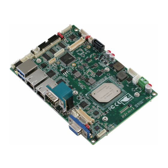
- Page 1 GENE-APL5 3.5” Subcompact Board User’s Manual 1 Last Updated: December 14, 2016...
-
Page 2: Copyright Notice
AAEON assumes no liabilities resulting from errors or omissions in this document, or from the use of the information contained herein. AAEON reserves the right to make changes in the product design without notice to its users. - Page 3 Acknowledgement All other products’ name or trademarks are properties of their respective owners. Microsoft Windows is a registered trademark of Microsoft Corp. Intel, Pentium, Celeron, and Xeon are registered trademarks of Intel Corporation Core, Atom are trademarks of Intel Corporation ...
- Page 4 Before setting up your product, please make sure the following items have been shipped: Item Quantity GENE-APL5 Product DVD with User’s Manual (in pdf) and drivers If any of these items are missing or damaged, please contact your distributor or sales representative immediately.
- Page 5 (if any), its specifications, dimensions, jumper/connector settings/definitions, and driver installation instructions (if any), to facilitate users in setting up their product. Users may refer to the AAEON.com for the latest version of this document. Preface...
- Page 6 Safety Precautions Please read the following safety instructions carefully. It is advised that you keep this manual for future references All cautions and warnings on the device should be noted. Make sure the power source matches the power rating of the device. Position the power cord so that people cannot step on it.
- Page 7 If any of the following situations arises, please the contact our service personnel: Damaged power cord or plug Liquid intrusion to the device iii. Exposure to moisture Device is not working as expected or in a manner as described in this manual The device is dropped or damaged Any obvious signs of damage displayed on the device...
- Page 8 FCC Statement This device complies with Part 15 FCC Rules. Operation is subject to the following two conditions: (1) this device may not cause harmful interference, and (2) this device must accept any interference received including interference that may cause undesired operation.
- Page 9 China RoHS Requirements (CN) 产品中有毒有害物质或元素名称及含量 AAEON Main Board/ Daughter Board/ Backplane 有毒有害物质或元素 部件名称 铅 汞 镉 六价铬 多溴联苯 多溴二苯醚 (Pb) (Hg) (Cd) (Cr(VI)) (PBB) (PBDE) 印刷电路板 ○ ○ ○ ○ ○ ○ 及其电子组件 外部信号 ○ ○ ○ ○ ○ ○...
- Page 10 China RoHS Requirement (EN) Poisonous or Hazardous Substances or Elements in Products AAEON Main Board/ Daughter Board/ Backplane Poisonous or Hazardous Substances or Elements Hexavalent Polybrominated Polybrominated Component Lead Mercury Cadmium Chromium Biphenyls Diphenyl Ethers (Pb) (Hg) (Cd) (Cr(VI)) (PBB) (PBDE) PCB &...
-
Page 11: Table Of Contents
Table of Contents Chapter 1 - Product Specifications ..................1 Specifications ......................2 Chapter 2 – Hardware Information ..................5 Dimensions ....................... 6 2.1.1 Dimensions (Optional HDMI SKU) ............. 8 Jumpers and Connectors ..................10 2.2.1 Jumpers and Connectors (Optional HDMI SKU)......12 Block Diagram ...................... - Page 12 2.5.5 External Power Input (CN5) ............... 23 2.5.6 External +5VSB Input (CN6) .............. 24 2.5.7 Audio I/O Port (CN7) ................24 2.5.8 LVDS Port 1 (CN8) ................25 2.5.9 COM Port 2 (CN9) ................26 2.5.10 LPT Port or Digital I/O Port (CN10) ..........28 2.5.11 LPC Port (CN11) ..................
- Page 13 2.5.33 Mini-Card Slot (Half-Mini) (CN33) ............ 48 2.5.34 mSATA (Full-Size) (CN34) ..............50 Chapter 3 - AMI BIOS Setup ....................53 System Test and Initialization ................54 AMI BIOS Setup ..................... 55 Setup submenu: Main ..................56 Setup submenu: Advanced ................. 57 3.4.1 Advanced: Trusted Computing ............
- Page 14 Product CD/DVD ....................84 Appendix A - Watchdog Timer Programming ..............86 Watchdog Timer Registers .................. 87 Watchdog Sample Program ................88 Appendix B - I/O Information ....................91 I/O Address Map ....................92 Memory Address Map ..................94 IRQ Mapping Chart ....................95 Appendix C –...
-
Page 15: Chapter 1 - Product Specifications
Chapter 1 Chapter 1 - Product Specifications... -
Page 16: Specifications
Specifications System 3.5” Form Factor Intel Pentium® N4200 / Celeron® N3350 ® Processor SoC Up to 2.5 GHz CPU Frequency Intel Atom™ N4200/ N3350 Processor SoC ® Chipset DDR3L 1867 Mhz SODIMM x 1 Memory Type ... - Page 17 Certification CE/FCC Display Intel Pentium® N4200 / Celeron® N3350 ® VGA/LCD Controller Processor SoC integrated VGA/LVDS/ LVDS2 (co-layout with HDMI, Video Output optional) Backlight Inverter Supply Intel® I210/I211, 10/100/1000Base-TX, RJ-45 x 2 Ethernet High definition audio interface Audio ...
- Page 18 1 (option) option Touch Chapter 1 – Product Specifications...
-
Page 19: Chapter 2 - Hardware Information
Chapter 2 Chapter 2 – Hardware Information... -
Page 20: Dimensions
Dimensions Component Side Chapter 2 – Hardware Information... - Page 21 Solder Side Chapter 2 – Hardware Information...
-
Page 22: Dimensions (Optional Hdmi Sku)
2.1.1 Dimensions (Optional HDMI SKU) Component Side Chapter 2 – Hardware Information... - Page 23 Solder Side Chapter 2 – Hardware Information...
-
Page 24: Jumpers And Connectors
Jumpers and Connectors Component Side Chapter 2 – Hardware Information... - Page 25 Solder Side Chapter 2 – Hardware Information...
-
Page 26: Jumpers And Connectors (Optional Hdmi Sku)
2.2.1 Jumpers and Connectors (Optional HDMI SKU) Component Side Chapter 2 – Hardware Information... - Page 27 Solder Side Chapter 2 – Hardware Information...
-
Page 28: Block Diagram
Block Diagram Chapter 2 – Hardware Information... -
Page 29: List Of Jumpers
List of Jumpers Please refer to the table below for all of the board’s jumpers that you can configure for your application Label Function LVDS Port1 Backlight Inverter VCC Selection and Operating VDD Selection LVDS Port1 Backlight Lightness Control Mode Selection COM2 Pin8 Function Selection COM3 Pin8 Function Selection Auto Power Button Enable/Disable Selection... -
Page 30: Lvds Port 1 Backlight Inverter Vcc Selection (Jp1)
2.4.1 LVDS Port 1 Backlight Inverter VCC Selection (JP1) +12V +5V (Default) 2.4.2 LVDS Port 1 Operating VDD Selection (JP1) +3.3V (Default) 2.4.3 LVDS Port 1 Backlight Lightness Control Mode Selection (JP2) 1 2 3 1 2 3 VR Mode (Default) PWM Mode 2.4.4 COM2 Pin8 Function Selection (JP3) Ring (Default) -
Page 31: Com3 Pin8 Function Selection (Jp4)
2.4.5 COM3 Pin8 Function Selection (JP4) Ring (Default) +12V 2.4.6 Auto Power Button Enable/Disable Selection (JP5) 1 2 3 1 2 3 Disable/ATX Enable/AT (Default) ※ When disabled, the power button of JP6 (1-2) will be used to power on the system. 2.4.7 Front Panel Connector (JP6) Pin Name Pin Name... -
Page 32: Lvds Port 2 Backlight Inverter Vcc Selection (Jp7)
2.4.8 LVDS Port 2 Backlight Inverter VCC Selection (JP7) +12V +5V (Default) 2.4.9 LVDS Port 2 Operating VDD Selection (JP7) +3.3V (Default) 2.4.10 LVDS Port 2 Backlight Lightness Control Mode Selection (JP8) 1 2 3 1 2 3 VR Mode (Default) PWM Mode 2.4.11 Touch Screen 4, 5, 8 Wire Selection (JP9) -
Page 33: Clear Cmos Jumper (Jp10)
2.4.12 Clear CMOS Jumper (JP10) 1 2 3 1 2 3 Normal (Default) Clear CMOS Chapter 2 – Hardware Information... -
Page 34: List Of Connectors
List of Connectors Please refer to the table below for all of the board’s connectors that you can configure for your application Label Function +5VSB Output w/SMBus LVDS Port1 Inverter / Backlight Connector +5V Output for SATA HDD SATA Port External Power Input External +5VSB Input Audio I/O Port... - Page 35 Label Function CN24 LVDS Port2 Inverter / Backlight Connector CN25 USB Ports 0 and 1 CN26 LAN (RJ-45) Port2 CN27 LAN (RJ-45) Port1 CN28 COM Port 1 (D-SUB 9) CN29 HDMI Port (Optional) CN30 Battery CN31 VGA Port CN32 Micro SIM Card Socket CN33 Mini-Card Slot (Half-Size) CN34...
-
Page 36: 5Vsb Output W/Smbus (Cn1)
2.5.1 +5VSB Output w/SMBus (CN1) SMB_DATA SMB_CLK PS_ON# +5VSB Pin Name Signal Type Signal level SMB_DATA +3.3V SMB_CLK +3.3V PS_ON# +5VSB 2.5.2 LVDS Port 1 Inverter / Backlight Connector (CN2) BLK_PWR BKL_CONTROL BKL_ENABLE Pin Name Signal Type Signal level BKL_PWR +5V / +12V BKL_CONTROL BKL_ENABLE... -
Page 37: Output For Sata Hdd (Cn3)
2.5.3 +5V Output for SATA HDD (CN3) Pin Name Signal Type Signal Level 2.5.4 SATA Port (CN4) Pin 1 Pin 7 Pin Name Signal Type Signal Level SATA_TX+ DIFF SATA_TX- DIFF SATA_RX- DIFF SATA_RX+ DIFF 2.5.5 External Power Input (CN5) +12V GND Chapter 2 –... -
Page 38: External +5Vsb Input (Cn6)
Pin Name Signal Type Signal Level +VIN 9V~19V or 12V ※There are two types of power input, 9V~19V or 12V only, by BOM Change. 2.5.6 External +5VSB Input (CN6) PS_ON# +5VSB Pin Name Signal Type Signal Level PS_ON# +5VSB 2.5.7 Audio I/O Port (CN7) MIC_L MIC_R GND_AUDIO... -
Page 39: Lvds Port 1 (Cn8)
Pin Name Signal Type Signal Level GND_AUDIO LEFT_OUT GND_AUDIO RIGHT_OUT +5V_AUDIO 2.5.8 LVDS Port 1 (CN8) PIN 29 PIN 30 PIN 1 PIN 2 *LVDS LCD_PWR can be set to +3.3V or +5V by JP1 Pin Name Signal Type Signal Level BKL_ENABLE BKL_CONTROL LCD_PWR... -
Page 40: Com Port 2 (Cn9)
Pin Name Signal Type Signal Level LVDS_DA0+ DIFF LVDS_DA1- DIFF LVDS_DA1+ DIFF LVDS_DA2- DIFF LVDS_DA2+ DIFF LVDS_DA3- DIFF LVDS_DA3+ DIFF DDC_DATA +3.3V DDC_CLK +3.3V LVDS_DB0- DIFF LVDS_DB0+ DIFF LVDS_DB1- DIFF LVDS_DB1+ DIFF LVDS_DB2- DIFF LVDS_DB2+ DIFF LVDS_DB3- DIFF LVDS_DB3+ DIFF LCD_PWR +3.3V/+5V LVDS_B_CLK-... - Page 41 RS-232 Pin Name Signal Type Signal Level DCD2 DSR2 RTS2 ±5V ±5V CTS2 DTR2 ±5V RI2/+5V/+12V +5V/+12V RS-485 Pin Name Signal Type Signal Level RS485_ D2- ±5V RS485_D2+ ±5V Chapter 2 – Hardware Information...
-
Page 42: Lpt Port Or Digital I/O Port (Cn10)
NC/+5V/+12V +5V/+12V RS-422 Pin Name Signal Type Signal Level RS422_TX2- ±5V RS422_TX2+ ±5V RS422_RX2+ RS422_RX2- NC/+5V/+12V +5V/+12V * COM2 RS-232/422/485 can be set by BIOS setting. Default is RS-232. * Pin 8 function can be set by JP3. 2.5.10 LPT Port or Digital I/O Port (CN10) STROBE# AFD# ERROR#... - Page 43 ※ LPT or Digital I/O function can be selected by BIOS setting. Default is Digital I/O. LPT Port Pin Name Signal Type Signal Level STROBE# AFD# ERROR# PRINT# SLIN# ACK# BUSY Chapter 2 – Hardware Information...
- Page 44 LPT Port Pin Name Signal Type Signal Level SLCT DIO0 DIO1 DIO2 DIO3 DIO4 DIO5 DIO6 DIO7 Digital I/O Port Pin Name Signal Type Signal Level DIO0 DIO1 DIO2 DIO3 DIO4 DIO5 Chapter 2 – Hardware Information...
-
Page 45: Lpc Port (Cn11)
Digital I/O Port Pin Name Signal Type Signal Level DIO6 DIO7 2.5.11 LPC Port (CN11) LAD0 LAD1 LAD2 LAD3 +3.3V LFRAME# LRESET# LCLK LDRQ0 LDRQ1 SERIRQ Pin Name Signal Type Signal Level LAD0 +3.3V LAD1 +3.3V LAD2 +3.3V Chapter 2 – Hardware Information... -
Page 46: Com Port 3 (Cn12)
LAD3 +3.3V +3.3V +3.3V LFRAME# LRESET# +3.3V LCLK LDRQ0 LDRQ1 SERIRQ +3.3V 2.5.12 COM Port 3 (CN12) RS-232 Pin Name Signal Type Signal Level DCD3 DSR3 RTS3 ±5V ±5V CTS3 Chapter 2 – Hardware Information... - Page 47 DTR3 ±5V RI3/+5V/+12V +5V/+12V RS-485 Pin Name Signal Type Signal Level RS485_ D3- ±5V RS485_D3+ ±5V NC/+5V/+12V +5V/+12V RS-422 Pin Name Signal Type Signal Level RS422_TX3- ±5V RS422_TX3+ ±5V RS422_RX3+ RS422_RX3- NC/+5V/+12V +5V/+12V Chapter 2 – Hardware Information...
-
Page 48: Bios Debug Port (Cn13)
* COM3 RS-232/422/485 can be set by BIOS setting. Default is RS-232. * Pin 8 function can be set by JP4. 2.5.13 BIOS Debug Port (CN13) P IN1 P IN2 P IN3 P IN4 P IN5 P IN6 P IN7 Pin Name Signal Type Signal Level... -
Page 49: Ps/2 Keyboard/Mouse Combo Port (Cn15)
Pin Name Signal Type Signal Level DCD4 DSR4 RTS4 ±9V ±9V CTS4 DTR4 ±9V 2.5.15 PS/2 Keyboard/Mouse Combo Port (CN15) KB_DATA KB_CLK +5VSB MS_CLK MS_DATA Pin Name Signal Type Signal Level KB_ DATA KB_CLK +5VSB MS_DATA Chapter 2 – Hardware Information... -
Page 50: Usb 2.0 Port 2 (Cn16)
MS_CLK 2.5.16 USB 2.0 Port 2 (CN16) +5VSB USB2_D- USB2_D+ Pin Name Signal Type Signal Level +5VSB USB_D- DIFF USB_D+ DIFF 2.5.17 USB 2.0 Port 3 (CN17) +5VSB USB3_D- USB3_D+ Pin Name Signal Type Signal Level +5VSB USB_D- DIFF USB_D+ DIFF Chapter 2 –... -
Page 51: Com Port 1 (Cn18) (Wafer, Opional)
2.5.18 COM Port 1 (CN18) (Wafer, Opional) Pin Name Signal Type Signal Level DCD1 DSR1 RTS1 ±9V ±9V CTS1 DTR1 ±9V 2.5.19 USB 2.0 Port 4 (CN19) +5VSB USB4_D- USB4_D+ Pin Name Signal Type Signal Level +5VSB Chapter 2 – Hardware Information... -
Page 52: Usb 2.0 Port 5 (Cn20)
USB_D- DIFF USB_D+ DIFF 2.5.20 USB 2.0 Port 5 (CN20) +5VSB USB5_D- USB5_D+ Pin Name Signal Type Signal Level +5VSB USB_D- DIFF USB_D+ DIFF 2.5.21 LVDS Port 2 (CN21) PIN 29 PIN 30 PIN 1 PIN 2 Chapter 2 – Hardware Information... - Page 53 *LVDS2 LCD_PWR can be set to +3.3V or +5V by JP7 Pin Name Signal Type Signal Level BKL_ENABLE BKL_CONTROL LCD_PWR +3.3V/+5V LVDS_A_CLK- DIFF LVDS_A_CLK+ DIFF LCD_PWR +3.3V/+5V LVDS_DA0- DIFF LVDS_DA0+ DIFF LVDS_DA1- DIFF LVDS_DA1+ DIFF LVDS_DA2- DIFF LVDS_DA2+ DIFF LVDS_DA3- DIFF LVDS_DA3+ DIFF...
-
Page 54: Touchscreen Connector (Cn22)
Pin Name Signal Type Signal Level LVDS_DB3+ DIFF LCD_PWR +3.3V/+5V LVDS_B_CLK- DIFF LVDS_B_CLK+ DIFF 2.5.22 Touchscreen Connector (CN22) TOP EXCITE BOTTOM EXCITE LEFT EXCITE RIGHT EXCITE TOP SENSE BOTTOM SENSE LEFT SENSE RIGHT SENSE 8-Wire Pin Name Signal Type Signal Level TOP EXCITE BOTTOM EXCITE LEFT EXCITE... - Page 55 BOTTOM LEFT RIGHT 4-Wire Pin Name Signal Type Signal Level BOTTOM LEFT RIGHT UL(Y) UR(H) LL(L) LR(X) SENSE(S) 5-Wire Pin Name Signal Type Signal Level UL(Y) Chapter 2 – Hardware Information...
-
Page 56: Cpu Fan (Cn23, Optional)
UR(H) LL(L) LR(X) SENSE(S) 2.5.23 CPU Fan (CN23, Optional) FAN_TAC FAN_POWER Pin Name Signal Type Signal Level FAN_POWER +12V FAN_TAC 2.5.24 LVDS Port 2 Inverter / Backlight Connector (CN24) BLK_PWR BKL_CONTROL BKL_ENABLE Pin Name Signal Type Signal level BKL_PWR +5V / +12V BKL_CONTROL Chapter 2 –... -
Page 57: Usb 3.0 Ports 0 And 1 (Cn25)
BKL_ENABLE * LVDS2 BKL_PWR can be set to +5V or +12V by JP7 * LVDS2 BKL_CONTROL can be set by JP8 2.5.25 USB 3.0 Ports 0 and 1 (CN25) Port 1 11 12 13 Port 0 2 3 4 Pin Name Signal Type Signal Level +5VSB... -
Page 58: Lan (Rj-45) Port 2 (Cn26)
USB_SSRX+ DIFF USB_SSTX− DIFF USB_SSTX+ DIFF 2.5.26 LAN (RJ-45) Port 2 (CN26) ACT/LINK SPEED Pin Name Signal Type Signal level MDI0+ DIFF MDI0- DIFF MDI1+ DIFF MDI2+ DIFF MDI2- DIFF MDI1- DIFF MDI3+ DIFF MDI3- DIFF 2.5.27 LAN (RJ-45) Port 1 (CN27) ACT/LINK SPEED Pin Name... -
Page 59: Com Port 1 (Cn28, D-Sub 9)
MDI0- DIFF MDI1+ DIFF MDI2+ DIFF MDI2- DIFF MDI1- DIFF MDI3+ DIFF MDI3- DIFF 2.5.28 COM Port 1 (CN28, D-SUB 9) Pin Name Signal Type Signal level ±9V ±9V ±9V 2.5.29 HDMI Port (CN29, Optional) Chapter 2 – Hardware Information... -
Page 60: Battery (Cn30)
Pin Name Signal Type Signal level TMDS_DAT2+ DIFF TMDS_DAT2- DIFF TMDS_DAT1+ DIFF TMDS_DAT1- DIFF TMDS_DAT0+ DIFF TMDS_DAT0- DIFF TMDS_CLK+ DIFF TMDS_CLK- DIFF DDC_CLK DDC_DATA HPLG_DETECT 2.5.30 Battery (CN30) Pin Name Signal Type Signal level +3.3V 3.3V Chapter 2 – Hardware Information... -
Page 61: Vga Port (Cn31)
2.5.31 VGA Port (CN31) Pin Name Signal Type Signal level GREEN BLUE RED_GND_RTN GREEN_GND_RTN BLUE_GND_RTN DDC_DATA HSYNC VSYNC DDC_CLK 2.5.32 Micro SIM Card Socket (CN32) Chapter 2 – Hardware Information... -
Page 62: Mini-Card Slot (Half-Mini) (Cn33)
Pin Name Signal Type Signal level UIM_PWR UIM_RST UIM_CLK UIM_VPP UIM_DATA 2.5.33 Mini-Card Slot (Half-Mini) (CN33) Pin Name Signal Type Signal level PCIE_WAKE# +3.3VSB +3.3V +1.5V +1.5V PCIE_CLK_REQ# UIM_PWR Chapter 2 – Hardware Information... - Page 63 Pin Name Signal Type Signal level UIM_DATA PCIE_REF_CLK- DIFF UIM_CLK PCIE_REF_CLK+ DIFF UIM_RST UIM_VPP W_DISABLE# +3.3V PCIE_RST# +3.3V PCIE_RX- DIFF +3.3VSB +3.3V PCIE_RX+ DIFF +1.5V +1.5V SMB_CLK +3.3V PCIE_TX- DIFF SMB_DATA +3.3V PCIE_TX+ DIFF Chapter 2 – Hardware Information...
-
Page 64: Msata (Full-Size) (Cn34)
Pin Name Signal Type Signal level USB_D- DIFF USB_D+ DIFF +3.3VSB +3.3V +3.3VSB +3.3V +1.5V +1.5V +3.3VSB +3.3V 2.5.34 mSATA (Full-Size) (CN34) ※ CN34 can be change to mini-card by BOM change. Pin Name Signal Type Signal Level +3.3V +3.3V Chapter 2 –... - Page 65 Pin Name Signal Type Signal Level +1.5V +1.5V SATA_RX+ DIFF +3.3V +3.3V SATA_RX- DIFF +1.5V +1.5V SMB_CLK +3.3V SATA_TX- DIFF Chapter 2 – Hardware Information...
- Page 66 Pin Name Signal Type Signal Level SMB_DATA +3.3V SATA_TX+ DIFF +3.3V +3.3V +3.3V +3.3V +1.5V +1.5V +3.3V +3.3V Chapter 2 – Hardware Information...
-
Page 67: Chapter 3 - Ami Bios Setup
Chapter 3 Chapter 3 - AMI BIOS Setup... -
Page 68: System Test And Initialization
System Test and Initialization The board uses certain routines to perform testing and initialization. If an error, fatal or non-fatal, is encountered, a few short beeps or an error message will be outputted. The board can usually continue the boot up sequence with non-fatal errors. The system configuration verification routines check the current system configuration against the values stored in the CMOS memory. -
Page 69: Ami Bios Setup
AMI BIOS Setup The AMI BIOS ROM has a pre-installed Setup program that allows users to modify basic system configurations, which is stored in the battery-backed CMOS RAM and BIOS NVRAM so that the information is retained when the power is turned off. To enter BIOS Setup, press <Del>... -
Page 70: Setup Submenu: Main
Setup submenu: Main Delete Press ‘ ’ Key to enter Setup Chapter 3 – AMI BIOS Setup... -
Page 71: Setup Submenu: Advanced
Setup submenu: Advanced Chapter 3 – AMI BIOS Setup... -
Page 72: 3.4.1 Advanced: Trusted Computing
3.4.1 Advanced: Trusted Computing Options summary: Security Device Disable Support Optimal Default, Failsafe Default Enable Enables or Disables BIOS support for security device. O.S. will not show Security Device. TCG EFI protocol and INT1A interface will not be available. SHA-1 PCR Bank Disable Optimal Default, Failsafe Default Enable... - Page 73 Pending Operation None Optimal Default, Failsafe Default TPM Clear Schedule an Operation for the Security Device. NOTE: Your Computer will reboot during restart in order to change State of Security Device. Platform Hierarchy Disabled Optimal Default, Failsafe Default Enabled Enable or disable Platform Hierarchy Storage Hierarchy Disabled Optimal Default, Failsafe Default...
-
Page 74: 3.4.2 Advanced: Cpu Management
3.4.2 Advanced: CPU Management Options summary: C-States Disabled Optimal Default, Failsafe Default Enabled Enable/Disable C States. EIST™ Disabled Optimal Default, Failsafe Default Enabled Enable/Disable Intel SpeedStep. Intel Virtualization Disabled Technology Optimal Default, Failsafe Default Enabled When enabled, a VMM can utilize the additional hardware capabilities provided by Vanderpool Technology. - Page 75 Enabled Enable/Disable CPU VT-d Thermal Monitor Disabled Optimal Default, Failsafe Default Enabled Enable/Disable Thermal Monitor Chapter 3 – AMI BIOS Setup...
-
Page 76: 3.4.3 Advanced: Hardware Monitor
3.4.3 Advanced: Hardware Monitor Options summary: Smart Fan Disable Optimal Default, Failsafe Default Enable Enables or Disables Smart Fan. Chapter 3 – AMI BIOS Setup... -
Page 77: Hardware Monitor: Cpu Smart Fan Mode
3.4.3.1 Hardware Monitor: CPU Smart Fan Mode Configuration Options summary: Fan 1 Smart Fan Manual RPM Mode Control Manual Duty Mode Auto RPM Mode Optimal Default, Failsafe Default Auto Duty-Cycle Mode Smart Fan Mode Select Temperature Source CPU Optimal Default, Failsafe Default CPU(external) System Select the monitored temperature source for this fan. - Page 78 Duty Cycle 1 Temperature 1 Auto fan speed control. Fan speed will follow different temperature by different duty cycle 1-100 Chapter 3 – AMI BIOS Setup...
-
Page 79: 3.4.4 Advanced: Sio Configuration
3.4.4 Advanced: SIO Configuration Chapter 3 – AMI BIOS Setup... -
Page 80: Sio Configuration: Serial Port 1 Configuration
3.4.4.1 SIO Configuration: Serial Port 1 Configuration Options summary: Use This Device Disable Optimal Default, Failsafe Default Enable Enable or Disable this Logical Device. Possible: Use Automatic Settings Optimal Default, Failsafe Default IO=3F8h; IRQ=4 IO=2F8h; IRQ=3 Allows user to change Device's Resource settings. New settings will be reflected on This Setup Page after System restarts. -
Page 81: Sio Configuration: Serial Port 2 Configuration
3.4.4.2 SIO Configuration: Serial Port 2 Configuration Options summary: Use This Device Disable Optimal Default, Failsafe Default Enable Enable or Disable this Logical Device. Possible: Use Automatic Settings Optimal Default, Failsafe Default IO=2F8h; IRQ=3 IO=3F8h; IRQ=4 Allows user to change Device's Resource settings. New settings will be reflected on This Setup Page after System restarts. -
Page 82: Sio Configuration: Serial Port 3 Configuration
3.4.4.3 SIO Configuration: Serial Port 3 Configuration Options summary: Use This Device Disable Optimal Default, Failsafe Default Enable Enable or Disable this Logical Device. Possible: Use Automatic Settings Optimal Default, Failsafe Default IO=3E8h; IRQ=11 IO=2E8h; IRQ=11 Allows user to change Device's Resource settings. New settings will be reflected on This Setup Page after System restarts. -
Page 83: Sio Configuration: Serial Port 4 Configuration
3.4.4.4 SIO Configuration: Serial Port 4 Configuration Options summary: Use This Device Disable Optimal Default, Failsafe Default Enable Enable or Disable this Logical Device. Possible: Use Automatic Settings Optimal Default, Failsafe Default IO=2E8h; IRQ=10 IO=3E8h; IRQ=10 Allows user to change Device's Resource settings. New settings will be reflected on This Setup Page after System restarts. -
Page 84: Sio Configuration: Parallel Port Configuration
3.4.4.5 SIO Configuration: Parallel Port Configuration Options summary: Use This Device Disable Optimal Default, Failsafe Default Enable Enable or Disable this Logical Device. Chapter 3 – AMI BIOS Setup... -
Page 85: 3.4.5 Advanced: Power Management
3.4.5 Advanced: Power Management Options summary: Power Mode ATX Type Optimal Default, Failsafe Default AT Type Select system power mode Power Saving(ERP) Disabled Optimal Default, Failsafe Default Control Enabled Configure power mode for power saving function. Restore AC Power Last State Optimal Default, Failsafe Default Loss Always On... - Page 86 RTC wake system Disable Optimal Default, Failsafe Default from S5 Fixed Time Dynamic Time Select system power mode Chapter 3 – AMI BIOS Setup...
-
Page 87: 3.4.6 Advanced: Digital Io Port Configuration
3.4.6 Advanced: Digital IO Port Configuration Options summary: DIO Port* Output Input Set DIO as Input or Output Output Level High Optimal Default, Failsafe Default Set output level when DIO pin is output Chapter 3 – AMI BIOS Setup... -
Page 88: Setup Submenu: Chipset
Setup submenu: Chipset Chapter 3 – AMI BIOS Setup... -
Page 89: 3.5.1 Chipset: North Bridge
3.5.1 Chipset: North Bridge Options summary: Max TOULD 2 GB Optimal Default, Failsafe Default 2.25 GB 2.5 GB 2.75 GB 2 GB Maximum Value of TOLUD. Chapter 3 – AMI BIOS Setup... -
Page 90: North Bridge: Lvds Panel Configuration
3.5.1.1 North Bridge: LVDS Panel Configuration * LVDS2 only available for 2 LVDS SKU Options summary: LVDS Disabled Enabled Optimal Default, Failsafe Default Enable/Disabled this panel. LVDS Panel Type 640x480,18bit,60Hz 800x480,18bit,60Hz 800x600,18bit,60Hz 1024x600,18bit,60Hz 1024x768,18bit,60Hz 1024x768,24bit,60Hz Optimal Default, Failsafe Default 1280x768,24bit,60Hz 1280x1024,48bit,60Hz Chapter 3 –... - Page 91 1366x768,24bit,60Hz 1440x900,48bit,60Hz 1600x1200,48bit,60Hz 1920x1080,48bit,60Hz 1920x1200,48bit,60Hz Select LCD panel used by Internal Graphics Device by selecting the appropriate setup item. Color Depth 18-bit Optimal Default, Failsafe Default 24-bit 36-bit 48-bit Select panel type Backlight Type Normal Optimal Default, Failsafe Default Inverted Select backlight control signal type Backlight Level Optimal Default, Failsafe Default...
- Page 92 Backlight PWM Freq 100Hz 200Hz 220Hz Optimal Default, Failsafe Default 500Hz 1KHz 2.2KHz 6.5KHz Select PWM frequency of backlight control signal Chapter 3 – AMI BIOS Setup...
-
Page 93: Setup Submenu: Security
Setup submenu: Security Change User/Administrator Password If an Administrator Password is set, it will be required during boot up, or when the user enters the Setup utility. Please Note that a User Password does not provide access to many of the features in the Setup utility. Select the password you wish to set, press Enter to open a dialog box to enter your password (you can enter no more than six letters or numbers). -
Page 94: Setup Submenu: Boot
Setup submenu: Boot Options summary: Quiet Boot Disabled Enabled Optimal Default, Failsafe Default EnableDisable showing boot logo. Monitor Mwait Disable Enabled Auto Optimal Default, Failsafe Default Enable/Disable Monitor Mwait. To install Linux OS, please set this item to disable. Ipv4 PXE Support Disabled Optimal Default, Failsafe Default Enabled... -
Page 95: Setup Submenu: Save & Exit
Setup submenu: Save & Exit Chapter 3 – AMI BIOS Setup... -
Page 96: Note For Users
Note for Users To Install Linux OS, set the Monitor Mwait to Disabled (Boot->Monitor Mwait->[Disabled]) EIST (Enhanced Intel SpeedStep Technology) default is Disabled, go to Advanced->CPU Configuration->EIST to change the setting if you want EIST function Enabled. Chapter 3 – AMI BIOS Setup... -
Page 97: Chapter 4 - Drivers Installation
Chapter 4 Chapter 4 – Drivers Installation... -
Page 98: Product Cd/Dvd
Product CD/DVD The GENE-APL5 comes with a product DVD that contains all the drivers and utilities you need to setup your product. Insert the DVD and follow the steps in the autorun program to install the drivers. In case the program does not start, follow the sequence below to install the drivers. - Page 99 Drivers will be installed automatically Step 5 – Install TXE Driver Open the Step5 - TXE folder followed by SetupTXE.exe Follow the instructions Drivers will be installed automatically Step 6 – Install Touch Driver Open the Step6 - Touch folder followed by Setup.exe Follow the instructions Drivers will be installed automatically Step 7 –...
-
Page 100: Appendix A - Watchdog Timer Programming
Appendix A Appendix A - Watchdog Timer Programming... -
Page 101: A.1 Watchdog Timer Registers
A.1 Watchdog Timer Registers Table 1 : Watch dog relative IO address Default Value Note I/O Base I/O Base address for Watchdog operation. 0xA10 Address This address is assigned by SIO LDN7, register 0x60-0x61. Table 2 : Watchdog relative register table Register Offset BitNum... -
Page 102: A.2 Watchdog Sample Program
A.2 Watchdog Sample Program ****************************************************************************** // WDT I/O operation relative definition (Please reference to Table 1) #define WDTAddr 0x510 // WDT I/O base address Void WDTWriteByte(byte Register, byte Value); byte WDTReadByte(byte Register); Void WDTSetReg(byte Register, byte Bit, byte Val); // Watch Dog relative definition (Please reference to Table 2) #define DevReg 0x00 // Device configuration register #define WDTRstBit 0x80 // Watchdog WDTRST# (Bit7) - Page 103 VOID AaeonWDTEnable (){ WDTEnableDisable(1); // Procedure : AaeonWDTConfig VOID AaeonWDTConfig (byte Counter, BOOLEAN Unit){ // Disable WDT counting WDTEnableDisable(0); // Clear Watchdog Timeout Status WDTClearTimeoutStatus(); // WDT relative parameter setting WDTParameterSetting(Timer, Unit); VOID WDTEnableDisable(byte Value){ If (Value == 1) WDTSetBit(TimerReg, EnableBit, 1); else WDTSetBit(TimerReg, EnableBit, 0);...
- Page 104 VOID WDTWriteByte(byte Register, byte Value){ IOWriteByte(WDTAddr+Register, Value); byte WDTReadByte(byte Register){ return IOReadByte(WDTAddr+Register); VOID WDTSetBit(byte Register, byte Bit, byte Val){ byte TmpValue; TmpValue = WDTReadByte(Register); TmpValue &= ~(1 << Bit); TmpValue |= Val << Bit; WDTWriteByte(Register, TmpValue); ******************************************************************************* Appendix A – Watchdog Timer Programming...
-
Page 105: Appendix B - I/O Information
Appendix B Appendix B - I/O Information... -
Page 106: I/O Address Map
I/O Address Map Appendix B – I/O Information... - Page 107 Appendix B – I/O Information...
-
Page 108: Memory Address Map
Memory Address Map Appendix B – I/O Information... -
Page 109: Irq Mapping Chart
IRQ Mapping Chart Appendix B – I/O Information... - Page 110 Appendix B – I/O Information...
- Page 111 Appendix B – I/O Information...
- Page 112 Appendix B – I/O Information...
- Page 113 Appendix B – I/O Information...
-
Page 114: Appendix C - Mating Connectors
Appendix C Appendix C – Mating Connectors... -
Page 115: List Of Mating Connectors And Cables
Serial Port Molex 51021-0900 1701090150 Cable Connector LPT or Parallel Port CN10 Digital I/O Molex 51110-2650 1701260200 Cable Connector SHR-12V-S- AAEON CN11 1703120130 Connector LPC Cable COM Port Serial Port CN12 Molex 51021-0900 1701090150 Cable Connector COM Port Serial Port CN14... - Page 116 Connector PS/2 KB/MS PS/2 KB/MS CN15 PHDR-06VS 1700060152 Connector Cable USB Port #2 CN16 Molex 51021-0500 USB Cable 1700050207 Connector USB Port #3 CN17 Molex 51021-0500 USB Cable 1700050207 Connector USB Port #4 CN19 Molex 51021-0500 USB Cable 1700050207 Connector USB Port #5 CN20 Molex...
-
Page 117: Appendix D - Digital I/O Ports
Appendix D Appendix D – Digital I/O Ports... -
Page 118: Digital I/O Register
Digital I/O Register Appendix D – Digital I/O Ports... - Page 119 Appendix D – Digital I/O Ports...
-
Page 120: Digital I/O Sample Code (4 In 4 Out, 2 Low 2 High)
Digital I/O Sample Code (4 in 4 out, 2 low 2 high) Outportb(0x2E,0x87); //enter configuration Outportb(0x2E,0x87); Outportb(0x2E,0x07); //set LDN Outportb(0x2F,0x06); Outportb(0x2E,0xA0); //GPIO set 5 register Outportb(0x2F,0xF0); Outportb(0x2E,0xA1); //GPIO output data register Outportb(0x2F,0x30); Outportb(0x2E,0xAA); //exit configuration Appendix D – Digital I/O Ports...
Need help?
Do you have a question about the GENE-APL5 and is the answer not in the manual?
Questions and answers