
Subscribe to Our Youtube Channel
Related Manuals for Aaeon GENE-A55E


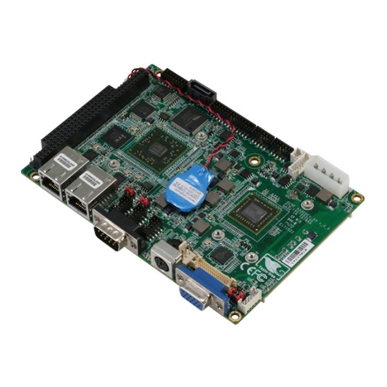
Summary of Contents for Aaeon GENE-A55E
- Page 1 S u b C o m p a c t B o a r d G E N E - A 5 5 E GENE-A55E AMD G-Series T16R Processor 10/100/1000Mb Ethernet 1 Mini-Card 4 USB2.0, 4 COM 2CH HD Audio GENE-A55E Manual 2 October, 2014...
-
Page 2: Copyright Notice
AAEON assumes no liabilities resulting from errors or omissions in this document, or from the use of the information contained herein. AAEON reserves the right to make changes in the product design without notice to its users. - Page 3 S u b C o m p a c t B o a r d G E N E - A 5 5 E Acknowledgments All other products’ name or trademarks are properties of their respective owners. AMI is a trademark of American Megatrends Inc. ...
-
Page 4: Packing List
Before you begin installing your card, please make sure that the following materials have been shipped: GENE-A55E CPU Card DVD-ROM for manual (in PDF format) and drivers If any of these items should be missing or damaged, please... -
Page 5: Table Of Contents
S u b C o m p a c t B o a r d G E N E - A 5 5 E Contents Chapter 1 General Information 1.1 Introduction ..............1-2 1.2 Features ..............1-3 1.3 Specifications ............1-4 Chapter 2 Quick Installation Guide 2.1 Safety Precautions ............ - Page 6 S u b C o m p a c t B o a r d G E N E - A 5 5 E 2.18 USB 2.0 Port 3 and Port 4 (CN5) ......2-17 2.19 USB 2.0 Port 1 and Port 2 (CN6) ......2-18 2.20 4P Power Connector Input (CN7) ......
- Page 7 S u b C o m p a c t B o a r d G E N E - A 5 5 E 3.2 AMI BIOS Setup ............3-3 Chapter 4 Driver Installation 4.1 Installation ..............4-3 Appendix A Programming The Watchdog Timer A.1 Programming ............
-
Page 8: Chapter 1 General Information
S u b C o m p a c t B o a r d G E N E - A 5 5 E Chapter General Information 1- 1 Chapter 1 General Information... -
Page 9: Introduction
USB2.0 x 4, COM ports x 4 (RS-232 x 2, RS-232/422/485 x 2) are configured on the GENE-A55E as well. Full functions make GENE-A55E a flexible and user friendly solution. This brand new SubCompact board is... -
Page 10: Features
S u b C o m p a c t B o a r d G E N E - A 5 5 E 1.2 Features AMD G-Series Single Core 615MHz Processor AMD A55E Chipset DDR3L SODIMM, 1066MHz Memory Up to 4 GB ... -
Page 11: Specifications
S u b C o m p a c t B o a r d G E N E - A 5 5 E 1.3 Specifications System Processor AMD G-series T16R single core 615 MHz System Memory 204-pin DDR3L 1066MHz SODIMM x 1, Max. - Page 12 S u b C o m p a c t B o a r d G E N E - A 5 5 E Board Size 5.75" x 4" (146mm x 101.6mm) Gross Weight 0.88 lb (0.4 kg) ...
- Page 13 S u b C o m p a c t B o a r d G E N E - A 5 5 E PS/2 Port Keyboard x 1, Mouse x 1 Audio Line-in, Line-out, Mic-in GPIO Up to 4 in and 4 out 1- 6 Chapter 1 General Information...
-
Page 14: Chapter 2 Quick Installation Guide
S u b C o m p a c t B o a r d G E N E - A 5 5 E Chapter Quick Installation Guide Chapter 2 Quick Installation Guide... -
Page 15: Safety Precautions
S u b C o m p a c t B o a r d G E N E - A 5 5 E 2.1 Safety Precautions Always completely disconnect the power cord from your board whenever you are working on it. -
Page 16: Location Of Connectors And Jumpers
S u b C o m p a c t B o a r d G E N E - A 5 5 E 2.2 Location of Connectors and Jumpers Component Side Component Side Chapter 2 Quick Installation Guide... -
Page 17: Solder Side
S u b C o m p a c t B o a r d G E N E - A 5 5 E Solder Side Chapter 2 Quick Installation Guide Solder Side... -
Page 18: Mechanical Drawing
S u b C o m p a c t B o a r d G E N E - A 5 5 E 2.3 Mechanical Drawing Component Side Component Side Chapter 2 Quick Installation Guide... - Page 19 S u b C o m p a c t B o a r d G E N E - A 5 5 E Solder Side Solder Side Chapter 2 Quick Installation Guide...
-
Page 20: List Of Jumpers
S u b C o m p a c t B o a r d G E N E - A 5 5 E 2.4 List of Jumpers The board has a number of jumpers that allow you to configure your system to suit your application. -
Page 21: List Of Connectors
S u b C o m p a c t B o a r d G E N E - A 5 5 E 2.5 List of Connectors The board has a number of connectors that allow you to configure your system to suit your application. - Page 22 S u b C o m p a c t B o a r d G E N E - A 5 5 E CN29 Realtek LAN (RJ-45) Port 1 CN30 Mini-Din PS/2 Connector CN31 COM Port 1 (D-SUB 9) CN32 VGA Port CN33...
-
Page 23: Setting Jumpers
S u b C o m p a c t B o a r d G E N E - A 5 5 E 2.6 Setting Jumpers You configure your card to match the needs of your application by setting jumpers. A jumper is the simplest kind of electric switch. It consists of two metal pins and a small metal clip (often protected by a plastic cover) that slides over the pins to connect them. -
Page 24: At/Atx Power Supply Mode Selection (Cn10)
S u b C o m p a c t B o a r d G E N E - A 5 5 E 2.7 AT/ATX Power Supply Mode Selection (CN10) 1 2 3 1 2 3 AT Mode (Default) ATX Mode CN10 Function... -
Page 25: Com2 Pin9 Function Selection (Cn17)
S u b C o m p a c t B o a r d G E N E - A 5 5 E CN16 Function +12V Ring (Default) 2.10 COM2 Pin9 Function Selection (CN17) Ring (Default) +12V CN17 Function +12V Ring (Default) 2.11 LVDS Backlight Inverter VCC Selection (CN24) -
Page 26: Lvds Backlight Lightness Control Mode Selection
S u b C o m p a c t B o a r d G E N E - A 5 5 E 2.12 LVDS Backlight Lightness Control Mode Selection (CN25) 1 2 3 1 2 3 VR Mode (Default) PWM Mode CN25 Function... -
Page 27: Sata Port (Cn2)
S u b C o m p a c t B o a r d G E N E - A 5 5 E 2.15 SATA Port (CN2) Pin 1 Pin 7 Pin Name Signal Type Signal level SATA_TX+ DIFF SATA_TX- DIFF SATA_RX-... -
Page 28: Audio I/O Port (Cn3)
S u b C o m p a c t B o a r d G E N E - A 5 5 E 2.16 Audio I/O Port (CN3) Pin Name Signal Signal level Type MIC_Vcc GND_AUDIO CD_GND LINE_L_IN CD_L LINE_R_IN CD_GND GND_AUDIO... -
Page 29: Lpt Port (Cn4)
S u b C o m p a c t B o a r d G E N E - A 5 5 E 2.17 LPT Port (CN4) LPT Mode DIO Mode STROBE# AFD# ERROR# DIO0 PRINT# DIO1 SLIN# DIO2 DIO3 ACK# DIO7... -
Page 30: Usb 2.0 Port 3 And Port 4 (Cn5)
S u b C o m p a c t B o a r d G E N E - A 5 5 E LPT Mode Pin Name Signal Type Signal level ACK# BUSY SLCT 2.18 USB 2.0 Port 3 and Port 4 (CN5) Pin Name Signal Type Signal level... -
Page 31: Usb 2.0 Port 1 And Port 2 (Cn6)
S u b C o m p a c t B o a r d G E N E - A 5 5 E USB2_D+ DIFF USB3_D+ DIFF USB3_D- DIFF +5VSB 2.19 USB 2.0 Port 1 and Port 2 (CN6) Pin Name Signal Type Signal level... -
Page 32: Power Connector Input (Cn7)
S u b C o m p a c t B o a r d G E N E - A 5 5 E 2.20 4P Power Connector Input (CN7) Pin Name Signal Type Signal level +12V +12V 2.21 External +5VSB Input (CN9) Pin Name Signal Type Signal level... -
Page 33: Pc/104 Slot (Cn14+Cn15)
S u b C o m p a c t B o a r d G E N E - A 5 5 E DIO2 +3.3V DIO3 +3.3V DIO4 +3.3V DIO5 +3.3V DIO6 +3.3V DIO7 +3.3V +3.3V +3.3V 2.23 PC/104 Slot (CN14+CN15) Pin Name Signal Type Signal level... - Page 34 S u b C o m p a c t B o a r d G E N E - A 5 5 E Pin Name Signal Type Signal level RSTDRV IRQ9 DRQ2 2-21 Chapter 2 Quick Installation Guide...
- Page 35 S u b C o m p a c t B o a r d G E N E - A 5 5 E Pin Name Signal Type Signal level ENDXFR# +12V +12V SMEMW# SMEMR# IOW# IOR# DACK3# DRQ3 DACK1# DRQ1 REFRESH# SYSCLK...
- Page 36 S u b C o m p a c t B o a r d G E N E - A 5 5 E Pin Name Signal Type Signal level SBHE# MEMR# MEMW# IN/OUT IN/OUT IN/OUT IN/OUT IN/OUT IN/OUT IN/OUT IN/OUT MEMCS16# 2-23...
- Page 37 S u b C o m p a c t B o a r d G E N E - A 5 5 E Pin Name Signal Type Signal level IOCS16# IRQ10 IRQ11 IRQ12 IRQ15 IRQ14 DACK0# DRQ0 DACK5# DRQ5 DACK6# DRQ6 DACK7#...
-
Page 38: Com Port 4(Cn18)
S u b C o m p a c t B o a r d G E N E - A 5 5 E 2.24 COM Port 4(CN18) Pin Name Signal Type Signal level ±9V ±9V ±9V 2.25 COM Port 3(CN19) 2-25 Chapter 2 Quick Installation Guide... - Page 39 S u b C o m p a c t B o a r d G E N E - A 5 5 E RS-232 Pin Name Signal Type Signal level ±9V ±9V ±9V RI/+5V/+12V IN/ PWR +5V/+12V +5V/+12V +5V/+12V RS-422 Pin Name Signal Type...
- Page 40 S u b C o m p a c t B o a r d G E N E - A 5 5 E RS-485 Pin Name Signal Type Signal level RS485_D- ±5V RS485_D+ ±5V NC/+5V/+12V +5V/+12V ※ COM3 RS-232/422/485 can be set by BIOS setting. Default is RS-232. ※...
-
Page 41: Com Port 2(Cn20)
S u b C o m p a c t B o a r d G E N E - A 5 5 E 2.26 COM Port 2 (CN20) RS-232 Pin Name Signal Type Signal level ±9V ±9V ±9V RI/+5V/+12V IN/ PWR +5V/+12V 2-28... - Page 42 S u b C o m p a c t B o a r d G E N E - A 5 5 E RS-422 Pin Name Signal Type Signal level ±5V RS422_TX- ±5V RS422_TX+ RS422_RX+ RS422_RX- NC/+5V/+12V +5V/+12V RS-485 Pin Name Signal Type Signal level...
-
Page 43: Lvds Port (Cn21)
S u b C o m p a c t B o a r d G E N E - A 5 5 E ※ COM2 RS-232/422/485 can be set by BIOS setting. Default is RS-232. ※ Pin 9 function can be set by CN17 2.27 LVDS Port (CN21) PIN 29 PIN 30... - Page 44 S u b C o m p a c t B o a r d G E N E - A 5 5 E Pin Name Signal Type Signal level LVDS_DA0- DIFF LVDS_DA0+ DIFF LVDS_DA1- DIFF LVDS_DA1+ DIFF LVDS_DA2- DIFF LVDS_DA2+ DIFF LVDS_DA3-...
-
Page 45: Lvds Inverter/ Backlight Connector (Cn22)
S u b C o m p a c t B o a r d G E N E - A 5 5 E 2.28 LVDS Inverter/ Backlight Connector (CN22) BLK_PWR BKL_CONTROL BKL_ENABLE Pin Name Signal Type Signal level BKL_PWR +5V / +12V BKL_CONTROL BKL_ENABLE... -
Page 46: Front Panel Connector (Cn27)
S u b C o m p a c t B o a r d G E N E - A 5 5 E 2.30 Front Panel Connector (CN27) Pin 1 PWR_BTN- Pin 2 PWR_BTN+ Pin 3 HDD_LED- Pin 4 HDD_LED+ Pin 5 SPEAKER-... -
Page 47: Realtek Lan (Rj-45) Port 2 (Cn28)
S u b C o m p a c t B o a r d G E N E - A 5 5 E 2.31 Realtek LAN (RJ-45) Port 2 (CN28) ACT/LINK SPEED Pin Name Signal Type Signal level DIFF MDI0+ DIFF MDI0-... -
Page 48: Mini-Din Ps/2 Keyboard/ Mouse Connector (Cn30)
S u b C o m p a c t B o a r d G E N E - A 5 5 E Pin Name Signal Type Signal level DIFF MDI0+ DIFF MDI0- DIFF MDI1+ DIFF MDI2+ DIFF MDI2- DIFF MDI1- DIFF... -
Page 49: Com Port 1 (Cn31)
S u b C o m p a c t B o a r d G E N E - A 5 5 E 2.34 COM Port 1 (CN31) Pin Name Signal Type Signal level ±9V ±9V ±9V 2.35 VGA Port (CN32) Pin Name Signal Type Signal level... - Page 50 S u b C o m p a c t B o a r d G E N E - A 5 5 E Pin Name Signal Type Signal level RED_GND_RTN GREEN_GND_RTN BLUE_GND_RTN DDC_DATA HSYNC VSYNC DDC_CLK 2-37 Chapter 2 Quick Installation Guide...
-
Page 51: Lpc Port (Cn33)
S u b C o m p a c t B o a r d G E N E - A 5 5 E 2.36 LPC Port (CN33) LAD0 LAD1 LAD2 LAD3 +3.3V LFRAME# LRESET# LCLK LDRQ0 LDRQ1 SERIRQ Pin Name Signal Type Signal level +3.3V... -
Page 52: Cfd Slot (Cn35)
S u b C o m p a c t B o a r d G E N E - A 5 5 E 2.37 CFD Slot (CN35) Pin Name Signal Type Signal level IN/OUT IN/OUT IN/OUT IN/OUT IN/OUT CS#0 +3.3V +3.3V IN/OUT... - Page 53 S u b C o m p a c t B o a r d G E N E - A 5 5 E Pin Name Signal Type Signal level IN/OUT CD1# IN/OUT IN/OUT IN/OUT IN/OUT IN/OUT CS#1 CF_IOR# CF_IOW# +3.3V +3.3V INTR...
-
Page 54: Mini-Card Slot (Cn36)
S u b C o m p a c t B o a r d G E N E - A 5 5 E Pin Name Signal Type Signal level IN/OUT IN/OUT IN/OUT 2.38 Mini-Card Slot (CN36) Pin Name Signal Type Signal level PCIE_WAKE# +3.3V... - Page 55 S u b C o m p a c t B o a r d G E N E - A 5 5 E Pin Name Signal Type Signal level W_DISABLE# +3.3V PCIE_RST# +3.3V PCIE_RX- DIFF +3.3VSB +3.3V PCIE_RX+ DIFF +1.5V +1.5V SMB_CLK...
- Page 56 S u b C o m p a c t B o a r d G E N E - A 5 5 E Pin Name Signal Type Signal level +3.3VSB +3.3V +1.5V +1.5V +3.3VSB +3.3V 2-43 Chapter 2 Quick Installation Guide...
-
Page 57: Uim Card Module (Cn37)
S u b C o m p a c t B o a r d G E N E - A 5 5 E 2.39 UIM Card Module (CN37) Pin Name Signal Type Signal level UIM_PWR UIM_RST UIM_CLK UIM_VPP UIM_DATA 2.40 DDR3L SODIMM Slot (DIMM1) Standard Specification 2-44... - Page 58 S u b C o m p a c t B o a r d G E N E - A 5 5 E China RoHS Requirements 产品中有毒有害物质或元素名称及含量 AAEON Main Board/ Daughter Board/ Backplane 有毒有害物质或元素 部件名称 铅 汞 镉 六价铬...
-
Page 59: Chapter 3 Ami Bios Setup
S u b C o m p a c t B o a r d G E N E - A 5 5 E Chapter BIOS Setup Chapter 3 AMI BIOS Setup 3-1... -
Page 60: System Test And Initialization
S u b C o m p a c t B o a r d G E N E - A 5 5 E 3.1 System Test and Initialization These routines test and initialize board hardware. If the routines encounter an error during the tests, you will either hear a few short beeps or see an error message on the screen. -
Page 61: Ami Bios Setup
S u b C o m p a c t B o a r d G E N E - A 5 5 E 3.2 AMI BIOS Setup AMI BIOS ROM has a built-in Setup program that allows users to modify the basic system configuration. -
Page 62: Setup Menu
S u b C o m p a c t B o a r d G E N E - A 5 5 E Setup Menu Setup submenu: Main Options summary: (default setting) System Date Day MM:DD:YYYY Change the month, year and century. The ‘Day’ is changed automatically. System Time hh : mm : ss Change the clock of the system. - Page 63 S u b C o m p a c t B o a r d G E N E - A 5 5 E Advanced Setup submenu: Options summary: (default setting) ACPI Settings System ACPI Parameters CPU Configuration CPU Configuration Parameters SATA Configuration SATA Device Options Settings USB Configuration...
-
Page 64: Acpi Settings
S u b C o m p a c t B o a r d G E N E - A 5 5 E F81866 Super IO Configuration System Super IO Chip Parameters. F81866 H/W Monitor Monitor hardware status ISA Configuration Configure IO or Memory address which will be decoded to ISA BUS IRQ Configuration Configure IRQs for ISA or PCI devices. -
Page 65: Rtc Wake Settings
S u b C o m p a c t B o a r d G E N E - A 5 5 E Options summary: (default setting) ACPI Sleep State S3 only(Suspend to RAM) Select the ACPI state used for System Suspend Enabled Wake on Ring Disabled... - Page 66 S u b C o m p a c t B o a r d G E N E - A 5 5 E Options summary: (default setting) Wake system with Fixed Disabled Time Enabled Enable or disable System wake on alarm event. Wake up time is setting by following settings.
-
Page 67: Cpu Configuration
S u b C o m p a c t B o a r d G E N E - A 5 5 E CPU Configuration SATA Configuration Chapter 3 AMI BIOS Setup 3-9... -
Page 68: Usb Configuration
S u b C o m p a c t B o a r d G E N E - A 5 5 E Options summary: (default setting) OnChip SATA Channel Disabled Enabled Enable or Disable Serial ATA OnChip SATA Type Legacy IDE AHCI Configure SATA controller operating as IDE/AHCI mode. - Page 69 S u b C o m p a c t B o a r d G E N E - A 5 5 E Auto Enables BIOS Support for Legacy USB Support. When enabled, USB can be functional in legacy environment like DOS. AUTO option disables legacy support if no USB devices are connected.
- Page 70 S u b C o m p a c t B o a r d G E N E - A 5 5 E F8 1866 Super IO Configuration Options summary: (default setting) Serial Port 1/2/3/4 Configuration Set Parameters of Serial Port 1/2/3/4 Parallel Port Configuration Set Parameters of Parallel Port Power Failure...
-
Page 71: Serial Port 1 Configuration
S u b C o m p a c t B o a r d G E N E - A 5 5 E Select AC power state when power is re-applied after a power failure. Serial Port 1 Configuration Options summary: (default setting) Serial Port Disabled... -
Page 72: Serial Port 2 Configuration
S u b C o m p a c t B o a r d G E N E - A 5 5 E IO=2E8h; IRQ=3,4,5,7,10,11,12; Select a resource setting for Super IO device. Serial Port 2 Configuration Options summary: (default setting) Serial Port Disabled Enabled... -
Page 73: Serial Port 3 Configuration
S u b C o m p a c t B o a r d G E N E - A 5 5 E IO=3E8h; IRQ=3,4,5,7,10,11,12; IO=2E8h; IRQ=3,4,5,7,10,11,12; Select a resource setting for Super IO device. Port Mode RS232 RS422 RS485 RS232/422,485 port mode switch Serial Port 3 Configuration... - Page 74 S u b C o m p a c t B o a r d G E N E - A 5 5 E Enabled En/Disable specified serial port. Change Settings Auto IO=3E8h; IRQ=11; IO=3E8h; IRQ=3,4,5,7,10,11,12; IO=2E8h; IRQ=3,4,5,7,10,11,12; IO=228h; IRQ=3,4,5,7,10,11,12; IO=220h;...
- Page 75 S u b C o m p a c t B o a r d G E N E - A 5 5 E Serial Port 4 Configuration Options summary: (default setting) Serial Port Disabled Enabled En/Disable specified serial port. Change Settings Auto IO=2E8h;...
-
Page 76: Parallel Port Configuration
S u b C o m p a c t B o a r d G E N E - A 5 5 E Parallel Port Configuration Options summary: (default setting) Parallel Port Disabled Enabled En/Disable specified parallel port. Change Settings Auto IO=378h;... - Page 77 S u b C o m p a c t B o a r d G E N E - A 5 5 E SPP Mode EPP-1.9 and SPP Mode EPP-1.7 and SPP Mode ECP Mode ECP and EPP 1.9 Mode ECP and EPP 1.7 Mode Change the Printer Port mode F81866 H/W Monitor...
-
Page 78: Cpu Fan Configuration
S u b C o m p a c t B o a r d G E N E - A 5 5 E CPU Fan Configuration Options summary: (default setting) Mode Control Auto Mode Full Speed CPU Fan mode select Temperature 1/2 1-100 Temperature setting for the boundary of the different fan speed level. - Page 79 S u b C o m p a c t B o a r d G E N E - A 5 5 E ISA Configuration Options summary: (default setting) 200h-27Fh/2C0h-20Fh/ Disabled 300h-37Fh/A79h-A79h/ FB80h-FBFFh/ Decoded to ISA FF80h-FFFFh Decode specified IO address to ISA BUS Subtractive decode agent Disabled Enabled...
- Page 80 S u b C o m p a c t B o a r d G E N E - A 5 5 E IRQ Configuration Options summary: (default setting) IRQ3/IRQ4/IRQ5/ Reserved IRQ7/IRQ10/IRQ11 For PCI Select specified IRQ can be used by PCI device or reserved for ISA devices. Chapter 3 AMI BIOS Setup 3-22...
- Page 81 S u b C o m p a c t B o a r d G E N E - A 5 5 E Digital IO Port Configuration Options summary: (default setting) Port1/Port2/Port3/Port4 Input Output Set DIO Port x as Input or Output Port5/Port6/Port7/Port8 Input Output...
- Page 82 S u b C o m p a c t B o a r d G E N E - A 5 5 E Setup submenu: Chipset Options summary: (default setting) North Bridge North Bridge Parameters South Bridge South Bridge Parameters Onboard Device Configure onboard devices Chapter 3 AMI BIOS Setup 3-24...
-
Page 83: North Bridge
S u b C o m p a c t B o a r d G E N E - A 5 5 E North Bridge Options summary: (default setting) Graphics Configuration Configure Graphics Setting Chapter 3 AMI BIOS Setup 3-25... -
Page 84: Graphics Configuration
S u b C o m p a c t B o a r d G E N E - A 5 5 E Graphics Configuration Options summary: (default setting) DP1 Output Mode LVDS Disabled Enabled/Disabled LVDS LVDS Panel 640x480,18bit,60Hz 800x480,18bit,60Hz 800x600,18bit,60Hz 1024x600,18bit,60Hz... - Page 85 S u b C o m p a c t B o a r d G E N E - A 5 5 E 1280x1024,48bit,60Hz 1366x768,24bit,60Hz 1440x900,48bit,60Hz 1600x1200,48bit,60Hz 1920x1080,48bit,60Hz 1920x1200,48bit,60Hz Select the resolution for LVDS Panel LVDS Backlight Level 100% Select the backlight level for LVDS Panel LVDS Backlight Type Normal...
-
Page 86: South Bridge
S u b C o m p a c t B o a r d G E N E - A 5 5 E South Bridge Options summary: (default setting) HD Audio Azalia Device Enabled Disabled Enable or Disable HD Audio Controller Power Mode ATX Type AT Type... -
Page 87: Onboard Device
S u b C o m p a c t B o a r d G E N E - A 5 5 E Onboard Device Options summary: (default setting) Onboard Gigabit LAN 1/2 Disabled Enabled Enable or Disable Onboard Gigabit LAN 1/2 Launch PXE OpROM Disabled Enabled... - Page 88 S u b C o m p a c t B o a r d G E N E - A 5 5 E Setup submenu: Boot Options summary: (default setting) Quiet Boot Disabled Enabled En/Disable showing boot logo. Launch RTL8111E PXE Disabled OpROM Enabled...
- Page 89 S u b C o m p a c t B o a r d G E N E - A 5 5 E BBS Priorities Options summary: (default setting) Boot Option #x Disabled Device name Sets the system boot order Chapter 3 AMI BIOS Setup 3-31...
- Page 90 S u b C o m p a c t B o a r d G E N E - A 5 5 E Setup submenu: Security Options summary: (default setting) Administrator Password/ Not set User Password You can install a Supervisor password, and if you install a supervisor password, you can then install a user password.
- Page 91 S u b C o m p a c t B o a r d G E N E - A 5 5 E Removing the Password: Highlight this item and type in the current password. At the next dialog box press Enter to disable password protection.
- Page 92 S u b C o m p a c t B o a r d G E N E - A 5 5 E Save as User Defaults Save the changes done so far as User Defaults Restore User Defaults Restore the User Defaults to all the setup options Boot Override Boot to specified device.
-
Page 93: Chapter 4 Driver Installation
S u b C o m p a c t B o a r d G E N E - A 5 5 E Chapter Driver Installation Chapter 4 Driver Installation... - Page 94 S u b C o m p a c t B o a r d G E N E - A 5 5 E The GENE-A55E comes with a DVD-ROM that contains all drivers and utilities that meet your needs.
- Page 95 S u b C o m p a c t B o a r d G E N E - A 5 5 E 4.1 Installation: Insert the GENE-A55E DVD-ROM into the DVD-ROM Drive. And install the drivers from Step 1 to Step 6 in order. Step 1 – Install Chipset Driver 1.
- Page 96 S u b C o m p a c t B o a r d G E N E - A 5 5 E Step 4 – Install AHCI Driver (Optional) This driver is needed when installing Windows XP with SATA in AHCI mode.
- Page 97 S u b C o m p a c t B o a r d G E N E - A 5 5 E Step 6 – Serial Port Driver (Optional) Please refer to readme.txt in the STEP6- Serial Port Driver (Optional) folder.
-
Page 98: Appendix A Programming The Watchdog Timer
S u b C o m p a c t B o a r d G E N E - A 5 5 E Appendix Programming the Watchdog Timer Appendix A Programming the Watchdog Timer A-1... -
Page 99: Programming
S u b C o m p a c t B o a r d G E N E - A 5 5 E A.1 Programming GENE-A55E utilizes FINTEK 81866 chipset as its watchdog timer controller. Below are the procedures to complete its configuration and the AAEON initial watchdog timer program is also attached based on which you can develop customized program to fit your application. - Page 100 S u b C o m p a c t B o a r d G E N E - A 5 5 E There are three steps to complete the configuration setup: (1) Enter the MB PnP Mode; (2) Modify the data of configuration registers; (3) Exit the MB PnP Mode.
- Page 101 S u b C o m p a c t B o a r d G E N E - A 5 5 E Watch Dog Timer 1, 2, 3 Control Register (Index=F5h,F6h,FAh Default=00h) Appendix A Programming the Watchdog Timer A-4...
-
Page 102: F81866 Watchdog Timer Initial Program
S u b C o m p a c t B o a r d G E N E - A 5 5 E A.2 F81866 Watchdog Timer Initial Program Main aaeonSuperIOOpen(); aaeonWdtSetCountMode(BOOL bMinute); // Set wdt count mode aaeonWdtSetTimeoutCount(BYTE tTimeout); // Set wdt timer aaeonWdtSetEnable(BOOL bEnable);... - Page 103 S u b C o m p a c t B o a r d G E N E - A 5 5 E Void aaeonWdtSetTimeoutCount(BYTE tTimeout){ f81866SetLdn(0x07); f81866WriteByte(F81866_WDT_TIME_REG, tTimeout); Void aaeonWdtSetEnable(BOOL bEnable){ f81866SetLdn(0x07); if(bEnable){ f81866WriteByte(0x30, 0x01); WDT_BASE_ADDR = (f81866ReadByte(F81866_WDT_BASEADDR_REG_MSB) << 8) | f81866ReadByte(F81866_WDT_BASEADDR_REG_LSB);...
- Page 104 S u b C o m p a c t B o a r d G E N E - A 5 5 E Void aaeonSuperIOClose(){ aaeonioWritePortByte(F81866_INDEX, 0xaa); Appendix A Programming the Watchdog Timer A-7...
-
Page 105: Appendix B I/O Information
S u b C o m p a c t B o a r d G E N E - A 5 5 E Appendix I/O Information Appendix B I/O Information... -
Page 106: I/O Address Map
S u b C o m p a c t B o a r d G E N E - A 5 5 E B.1 I/O Address Map Appendix B I/O Information... - Page 107 S u b C o m p a c t B o a r d G E N E - A 5 5 E Appendix B I/O Information...
-
Page 108: St Mb Memory Address Map
S u b C o m p a c t B o a r d G E N E - A 5 5 E B.2 1 MB Memory Address Map Appendix B I/O Information... -
Page 109: Irq Mapping Chart
S u b C o m p a c t B o a r d G E N E - A 5 5 E B.3 IRQ Mapping Chart B.4 DMA Channel Assignments Appendix B I/O Information... -
Page 110: Appendix C Mating Connector
S u b C o m p a c t B o a r d G E N E - A 5 5 E Appendix Mating Connector C - 1 Appendix C Mating Connector... -
Page 111: List Of Mating Connectors And Cables
S u b C o m p a c t B o a r d G E N E - A 5 5 E C.1 List of Mating Connectors and Cables The table notes mating connectors and available cables. Mating Connector Connector Available Function... - Page 112 S u b C o m p a c t B o a r d G E N E - A 5 5 E Connector Digital I/O CN13 Neltron 2026B-10 Connector COM Port 4 PINRE Serial Port 1701100206 CN18 52A-90-10GB00 Connector Cable COM Port 3...
-
Page 113: Appendix D Ahci Setting
S u b C o m p a c t B o a r d G E N E - A 5 5 E Appendix AHCI Settings Appendix D AHCI Settings... -
Page 114: Setting Ahci
S u b C o m p a c t B o a r d G E N E - A 5 5 E D.1 Setting AHCI OS installation to SETUP AHCI Mode Step 1: Copy files from “Driver DVD -> Step4 – AHCI(Optional)\WinXP_32”... - Page 115 S u b C o m p a c t B o a r d G E N E - A 5 5 E Step 7: Choose “AMD AHCI Compatible RAID Controller-x86 platform” for Windows XP 32-bit system; “AMD AHCI Compatible RAID Controller-x64 platform”...
Need help?
Do you have a question about the GENE-A55E and is the answer not in the manual?
Questions and answers