
Related Manuals for Aaeon GENE-8310


Summary of Contents for Aaeon GENE-8310
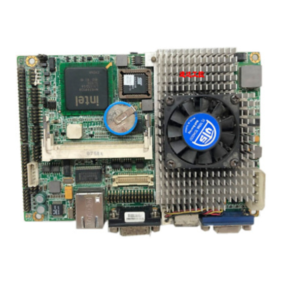
- Page 1 S u b C o m p a c t B o a r d G E N E - 8 3 1 0 GENE-8310 ® ® Intel Celeron M Processor SubCompact Board 18/24-bit Dual-channel LVDS Ethernet, 2 Channel Audio & Mini PCI GENE-8310 Rev. A Manual 5th Ed. February 2012...
-
Page 2: Copyright Notice
AAEON assumes no liabilities resulting from errors or omissions in this document, or from the use of the information contained herein. AAEON reserves the right to make changes in the product design without notice to its users. - Page 3 S u b C o m p a c t B o a r d G E N E - 8 3 1 0 Acknowledgments All other products’ name or trademarks are properties of their respective owners. Award is a trademark of Award Software International, Inc. ...
-
Page 4: Packing List
G E N E - 8 3 1 0 Packing List Before you begin installing your card, please make sure that the following materials have been shipped: 1 GENE-8310 CPU Card (with thermal solution) 1 Cable Kit 1 Jumper Cap ... -
Page 5: Table Of Contents
S u b C o m p a c t B o a r d G E N E - 8 3 1 0 Contents Chapter 1 General Information 1.1 Introduction..............1-2 1.2 Features ..............1-4 1.3 Specifications ............1-5 Chapter 2 Quick Installation Guide 2.1 Safety Precautions ............ - Page 6 S u b C o m p a c t B o a r d G E N E - 8 3 1 0 2.18 Dual Channel LVDS Connector (CN8)....2-15 2.19 4P Power Connector (CN9) ........2-16 2.20 Audio Input/Output Connector (CN12) ....2-16 2.21 Ethernet 10/100 Base-TX RJ-45 Phone Jack Connector (CN13) ................
- Page 7 S u b C o m p a c t B o a r d G E N E - 8 3 1 0 Appendix B I/O Information B.1 I/O Address Map ............B-2 B.2 1 MB Memory Address Map ........B-2 B.3 IRQ Mapping Chart ..........B-3 B.4 DMA Channel Assignments........B-3 Appendix C Mating Connector...
-
Page 8: Chapter 1 General Information
S u b C o m p a c t B o a r d G E N E - 8 3 1 0 Chapter General Information 1- 1 Chapter 1 General Information... -
Page 9: Introduction
AAEON has released through their original design. It is more advanced than previous SubCompact Boards, with higher performance and lower power consumption. We believe the GENE-8310 will become one of the best choices for our customers who need a higher requirement in processor ability with excellent power consumption control. - Page 10 SubCompact Board for sophisticated graphics output. Wide Expansion Capability Although the GENE-8310 measures only 5.75” x 4”, that does not affect its expansion ability because of the presence of an onboard Mini PCI slot. Hence, the GENE-8310 allows a greater variety of expansion interfaces in a very small space.
-
Page 11: Features
S u b C o m p a c t B o a r d G E N E - 8 3 1 0 1.2 Features ® ® Onboard Intel Celeron M 1.5GHz/ 1.3GHz/ ULV ® ® Intel Celeron M Processor at 600MHz &... -
Page 12: Specifications
S u b C o m p a c t B o a r d G E N E - 8 3 1 0 1.3 Specifications System ® ® Onboard Intel Celeron Processor 1.5GHz/ 1.3GHz or ® ® Intel ULV Celeron M Processor 1.0GHz 0K L2 Cache / 600MHz... - Page 13 S u b C o m p a c t B o a r d G E N E - 8 3 1 0 Power Supply +5V, AT/ATX Voltage Board Size 5.75”(L) x 4”(W) (146mm x 101.6mm) Gross Weight 0.88 lb (0.4 kg) ...
- Page 14 S u b C o m p a c t B o a r d G E N E - 8 3 1 0 USB: Two 5 x 2 Pin Headers Support 4 USB 2.0 Ports (Does not support Wake-up function) Chapter 1 General Information...
-
Page 15: Chapter 2 Quick Installation Guide
S u b C o m p a c t B o a r d G E N E - 8 3 1 0 Chapter Quick Installation Guide Chapter 2 Quick Installation Guide... -
Page 16: Safety Precautions
S u b C o m p a c t B o a r d G E N E - 8 3 1 0 2.1 Safety Precautions Always completely disconnect the power cord from your board whenever you are working on it. -
Page 17: Location Of Connectors And Jumpers
S u b C o m p a c t B o a r d G E N E - 8 3 1 0 2.2 Location of Connectors and Jumpers Component Side CN19 CN17 CN16 CN18 CN11 CN10 CN13 CN15 MPCI1 Chapter 2 Quick Installation Guide... - Page 18 S u b C o m p a c t B o a r d G E N E - 8 3 1 0 Solder Side CFD1 DIMM1 Chapter 2 Quick Installation Guide...
-
Page 19: Mechanical Drawing
S u b C o m p a c t B o a r d G E N E - 8 3 1 0 2.3 Mechanical Drawing Component Side (17.50) (6.50) (1.60) 137.16 137.16 133.93 133.93 114.94 114.30 109.22 90.17 79.37 72.39 54.15... - Page 20 S u b C o m p a c t B o a r d G E N E - 8 3 1 0 Solder Side 8.89 8.89 0.00 0.00 72.39 109.22 114.30 133.93 133.93 Chapter 2 Quick Installation Guide...
-
Page 21: List Of Jumpers
S u b C o m p a c t B o a r d G E N E - 8 3 1 0 2.4 List of Jumpers The board has a number of jumpers that allow you to configure your system to suit your application. -
Page 22: List Of Connectors
S u b C o m p a c t B o a r d G E N E - 8 3 1 0 2.5 List of Connectors The board has a number of connectors that allow you to configure your system to suit your application. - Page 23 S u b C o m p a c t B o a r d G E N E - 8 3 1 0 VBAT2 External Battery MPCI1 Mini PCI Slot CFD1 Compact Flash Disk Slot Chapter 2 Quick Installation Guide...
-
Page 24: Setting Jumpers
S u b C o m p a c t B o a r d G E N E - 8 3 1 0 2.6 Setting Jumpers You configure your card to match the needs of your application by setting jumpers. A jumper is the simplest kind of electric switch. It consists of two metal pins and a small metal clip (often protected by a plastic cover) that slides over the pins to connect them. -
Page 25: Clear Cmos Selection (Jp1)
S u b C o m p a c t B o a r d G E N E - 8 3 1 0 2.7 Clear CMOS Selection (JP1) Function Normal (Default) Clear CMOS 2.8 LCD Voltage Selection (JP2) Function +3.3V (Default) 2.9 COM2 RI/+5V Selection (JP5) Function... -
Page 26: Usb2.0 Port 2 Connector (Cn2)
S u b C o m p a c t B o a r d G E N E - 8 3 1 0 2.12 USB2.0 Port 2 Connector (CN2) Signal Signal USBVDD2-3 USBGND USBD2- USBGND USBD2+ USBD3+ USBGND USBD3- USBGND USBVDD2-3 2.13 Primary IDE Hard Drive Connector (CN3) -
Page 27: Digital Io Connector (Cn4)
S u b C o m p a c t B o a r d G E N E - 8 3 1 0 IRQ14 PDA1 P66DET PDA0 PDA2 PDCS#1 PDCS#3 IDEACTP# Ground +5Volt. +5Volt. Ground 2.14 Digital IO Connector (CN4) Name Name DIO_IN0... -
Page 28: Front Panel (Cn5)
S u b C o m p a c t B o a r d G E N E - 8 3 1 0 2.15 Front Panel (CN5) Signal ATX Power-on Button HDD Active LED External Speaker Power LED 9-10 System Reset Button 2.16 Serial Port COM2 Connector (CN6) COM2/ RS-232 Mode... -
Page 29: Parallel Port Connector (Cn7)
S u b C o m p a c t B o a r d G E N E - 8 3 1 0 Ground Note: COM mode-RS-232/422/485, selected by BIOS. 2.17 Parallel Port Connector (CN7) Signal Signal STBX AFD# PTD0 ERR# PTD1... -
Page 30: Power Connector (Cn9)
S u b C o m p a c t B o a r d G E N E - 8 3 1 0 TXL1# TXL1 TXL2# TXL2 TXL3# TXL3 LVDS_DATA LVDS_CLK TXU0# TXU0 TXU1# TXU1 TXU2# TXU2 TXU3# TXU3 LCD Volt. -
Page 31: Ethernet 10/100 Base-Tx Rj-45 Phone Jack Connector
S u b C o m p a c t B o a r d G E N E - 8 3 1 0 2.21 Ethernet 10/100Base-TX RJ-45 Phone Jack Connector (CN13) Signal Signal LINK_LED ACT_LED SPD_LED +3.3 Volt. 2.22 External 5VSB/PWRGD Connector (CN14) Signal Ground Ground... -
Page 32: Fan Connector (Cn16)
S u b C o m p a c t B o a r d G E N E - 8 3 1 0 2.24 Fan Connector (CN16) Signal FAN Sense +5 Volt. Ground 2.25 Mini-DIN PS/2 Connector (CN17) Signal Signal Keyboard Data Mouse Data... -
Page 33: External Battery (Vbat2)
S u b C o m p a c t B o a r d G E N E - 8 3 1 0 VGA Ground CRT_HSYNC VGA Ground CRT_VSYNC VGA Ground CRT_SCL VGA Ground 2.28 External Battery (VBAT2) Signal VBAT (+3 Volt.) Ground 2.29 Mini PCI Slot (MPCI1) - Page 34 S u b C o m p a c t B o a r d G E N E - 8 3 1 0 Ground Ground Ground Ground Ground Ground Ground Ground SDA2 SDA2 SDA1 SDA1 SDA0 SDA0 SDD0 SDD0 SDD1 SDD1 SDD2...
- Page 35 S u b C o m p a c t B o a r d G E N E - 8 3 1 0 Below Table for China RoHS Requirements 产品中有毒有害物质或元素名称及含量 AAEON Main Board/ Daughter Board/ Backplane 有毒有害物质或元素 部件名称 铅...
-
Page 36: Chapter 3 Award Bios Setup
S u b C o m p a c t B o a r d G E N E - 8 3 1 0 Chapter Award BIOS Setup Chapter 3 Award BIOS Setup... -
Page 37: System Test And Initialization
3. The CMOS memory has lost power and the configuration information has been erased. The GENE-8310 CMOS memory has an integral lithium battery backup for data retention. However, you will need to replace the complete unit when it finally runs down. -
Page 38: Award Bios Setup
S u b C o m p a c t B o a r d G E N E - 8 3 1 0 3.2 Award BIOS Setup Awards BIOS ROM has a built-in Setup program that allows users to modify the basic system configuration. This type of information is stored in battery-backed CMOS RAM so that it retains the Setup information when the power is turned off. - Page 39 Save CMOS value changes to CMOS and exit setup. Exit Without Saving Abandon all CMOS value changes and exit setup. You can refer to the "AAEON BIOS Item Description.pdf" file in the CD for the meaning of each setting in this chapter. Chapter 3 Award BIOS Setup...
-
Page 40: Chapter 4 Driver Installation
S u b C o m p a c t B o a r d G E N E - 8 3 1 0 Chapter Driver Installation Chapter 4 Driver Installation... - Page 41 S u b C o m p a c t B o a r d G E N E - 8 3 1 0 The GENE-8310 comes with a CD-ROM that contains all drivers and utilities that meet your needs.
- Page 42 S u b C o m p a c t B o a r d G E N E - 8 3 1 0 4.1 Installation: Insert the GENE-8310 CD-ROM into the CD-ROM Drive. And install the drivers from Step 1 to Step 4 in order. ®...
- Page 43 S u b C o m p a c t B o a r d G E N E - 8 3 1 0 Step 4 – Install Realtek AC97 codec Driver 1. Click on the Realtek AC97 codec Driver folder and then double click on the setup.exe 2.
-
Page 44: Appendix A Programming The Watchdog Timer
S u b C o m p a c t B o a r d G E N E - 8 3 1 0 Appendix Programming the Watchdog Timer Appendix A Programming the Watchdog Timer... -
Page 45: Programming
S u b C o m p a c t B o a r d G E N E - 8 3 1 0 A.1 Programming GENE-8310 utilizes ITE 8712 chipset as its watchdog timer controller. Below are the procedures to complete its configuration and the AAEON intial watchdog timer program is also attached based on which you can develop customized program to fit your application. - Page 46 S u b C o m p a c t B o a r d G E N E - 8 3 1 0 occur if the MB PnP Mode is not exited normally. (1) Enter the MB PnP Mode To enter the MB PnP Mode, four special I/O write operations are to be performed during Wait for Key state.
- Page 47 S u b C o m p a c t B o a r d G E N E - 8 3 1 0 WatchDog Timer Configuration Registers Configure Control (Index=02h) This register is write only. Its values are not sticky; that is to say, a hardware reset will automatically clear the bits, and does not require the software to clear them.
- Page 48 S u b C o m p a c t B o a r d G E N E - 8 3 1 0 WatchDog Timer Control Register (Index=71h, Default=00h) WatchDog Timer Configuration Register (Index=72h, Default=00h) WatchDog Timer Time-out Value Register (Index=73h, Default=00h) Appendix A Programming the Watchdog Timer...
- Page 49 S u b C o m p a c t B o a r d G E N E - 8 3 1 0 A.2 ITE8712 Watchdog Timer Initial Program .MODEL SMALL .CODE Main: CALL Enter_Configuration_mode CALL Check_Chip mov cl, 7 call Set_Logic_Device ;time setting mov cl, 10 ;...
- Page 50 S u b C o m p a c t B o a r d G E N E - 8 3 1 0 ; game port enable mov cl, 9 call Set_Logic_Device Initial_OK: CALL Exit_Configuration_mode MOV AH,4Ch INT 21h Enter_Configuration_Mode PROC NEAR MOV SI,WORD PTR CS:[Offset Cfg_Port] MOV DX,02Eh...
- Page 51 S u b C o m p a c t B o a r d G E N E - 8 3 1 0 Exit_Configuration_Mode ENDP Check_Chip PROC NEAR MOV AL,20h CALL Read_Configuration_Data CMP AL,87h JNE Not_Initial MOV AL,21h CALL Read_Configuration_Data CMP AL,12h JNE Not_Initial Need_Initial:...
- Page 52 S u b C o m p a c t B o a r d G E N E - 8 3 1 0 MOV DX,WORD PTR CS:[Cfg_Port+06h] IN AL,DX Read_Configuration_Data ENDP Write_Configuration_Data PROC NEAR MOV DX,WORD PTR CS:[Cfg_Port+04h] OUT DX,AL XCHG AL,AH MOV DX,WORD PTR CS:[Cfg_Port+06h] OUT DX,AL...
- Page 53 S u b C o m p a c t B o a r d G E N E - 8 3 1 0 Set_Logic_Device proc near push ax push cx xchg al,cl mov cl,07h call Superio_Set_Reg pop cx pop ax Set_Logic_Device endp ;Select 02Eh->Index Port, 02Fh->Data Port Cfg_Port DB 087h,001h,055h,055h...
-
Page 54: Appendix B I/O Information
S u b C o m p a c t B o a r d G E N E - 8 3 1 0 Appendix I/O Information Appendix B I/O Information... -
Page 55: I/O Address Map
S u b C o m p a c t B o a r d G E N E - 8 3 1 0 B.1 I/O Address Map Address Description User Address 000-01F DMA Controller #1 000-000F 020-03F Interrupt Controller #1, Master 020-021 040-05F System Time... -
Page 56: Irq Mapping Chart
S u b C o m p a c t B o a r d G E N E - 8 3 1 0 B.3 IRQ Mapping Chart IRQ0 System Timer IRQ8 System CMOS / Real time clock IRQ1 Keyboard IRQ9 Microsoft ACPI –... -
Page 57: Appendix C Mating Connector
S u b C o m p a c t B o a r d G E N E - 8 3 1 0 Appendix Mating Connector C - 1 Appendix C Mating Connector... -
Page 58: List Of Mating Connectors And Cables
S u b C o m p a c t B o a r d G E N E - 8 3 1 0 C.1 List of Mating Connectors and Cables The table notes mating connectors and available cables. Connector Function Mating Connector Available... - Page 59 S u b C o m p a c t B o a r d G E N E - 8 3 1 0 IrDA Neltron 2026A-06 CN15 Connector CPU FAN CN16 Ho-Base 2503-H-3 Connector Mini-Din Keyboard MD06F011 PS/2 & Mouse CN17 Catch 1700060192...
Need help?
Do you have a question about the GENE-8310 and is the answer not in the manual?
Questions and answers