Table of Contents
Advertisement
Quick Links
Advertisement
Table of Contents

Subscribe to Our Youtube Channel
Related Manuals for Aaeon GENE-5315


Summary of Contents for Aaeon GENE-5315
- Page 1 G E N E - 5 3 1 5 GENE-5315 ® Geode LX800/900 series Processors RTL8139DL for 10/100Mbps Type II CompactFlash 2 COM (Rev.A), 5 COM (Rev.B) 4 USB2.0, 1 IrDA Type III Mini PCI GENE-5315 Manual Rev.A + B 4th Ed. November 2009...
-
Page 2: Copyright Notice
AAEON assumes no liabilities resulting from errors or omissions in this document, or from the use of the information contained herein. AAEON reserves the right to make changes in the product design without notice to its users. - Page 3 S u b C o m p a c t B o a r d G E N E - 5 3 1 5 Acknowledgments All other products’ name or trademarks are properties of their respective owners. Award is a trademark of Award Software International, Inc. CompactFlash™...
-
Page 4: Packing List
G E N E - 5 3 1 5 Packing List Before you begin installing your card, please make sure that the following materials have been shipped: • 1 9681531501 Cable Kit for GENE-5315 1700060192 Keyboard & Mouse Cable 1709100201 USB Cable 1701440500 IDE Cable 3.5” •... -
Page 5: Table Of Contents
S u b C o m p a c t B o a r d G E N E - 5 3 1 5 Contents Chapter 1 General Information 1.1 Introduction..............1-2 1.2 Features ..............1-3 1.3 Specifications ............1-4 Chapter 2 Quick Installation Guide 2.1 Safety Precautions ............ - Page 6 S u b C o m p a c t B o a r d G E N E - 5 3 1 5 2.17 USB Port #1 and Port #2 (CN5) ......2-17 2.18 Digital I/O Connector (CN6) ........2-17 2.19 Audio Input/Output/Cdin/MIC (CN7)......
- Page 7 S u b C o m p a c t B o a r d G E N E - 5 3 1 5 2.40 Compact Flash Disk Slot (CFD1) ......2-29 2.41 Mini-PCI Slot (MPCI1) ........... 2-30 2.42 DDR SODIMM Slot (DIMM1) ......... 2-30 Chapter 3 Award BIOS Setup 3.1 System Test and Initialization.
-
Page 8: B.5 Dma Channel Assignments
S u b C o m p a c t B o a r d G E N E - 5 3 1 5 B.5 DMA Channel Assignments........B-3 Appendix C Mating Connector C.1 List of Mating Connectors and Cables....C-2... -
Page 9: Chapter 1 General Information
S u b C o m p a c t B o a r d G E N E - 5 3 1 5 Chapter General Information 1- 1 Chapter 1 General Information... -
Page 10: Introduction
Type III Mini PCI socket for expansion. Moreover, four USB 2.0, IDE, RS-232, RS-232/422/485 and parallel ports are configured on the GENE-5315. Full functions make GENE-5315 user friendly. With the GENE-5315, there are no more worries about installing many necessary devices to complete the functions of your system. -
Page 11: Features
S u b C o m p a c t B o a r d G E N E - 5 3 1 5 1.2 Features Onboard AMD Geode LX 800/LX900 processors SODIMM DDR 333 Max. 1GB, DDR 400 Max. 512MB Up to 24-bit Single Channel LVDS TFT LCD Dual 10/100Mbps Ethernet Type III Mini-PCI and PC/104 (For Rev.A Only) Expansions... -
Page 12: Specifications
S u b C o m p a c t B o a r d G E N E - 5 3 1 5 1.3 Specifications System Processor Onboard AMD Geode LX800/ LX900 Series Processor System Memory 200-pin DDR SODIMM x 1, Max. - Page 13 S u b C o m p a c t B o a r d G E N E - 5 3 1 5 Display Supports CRT/LCD simultaneous display Chipset AMD LX series + TI SN75LVDS83 Memory Shared system memory up to 254 MB LCD Interface Up to 24-bit TTL/LVDS TFT LCD Resolution...
-
Page 14: Chapter 2 Quick Installation Guide
S u b C o m p a c t B o a r d G E N E - 5 3 1 5 Chapter Quick Installation Guide Notice: The Quick Installation Guide is derived from Chapter 2 of user manual. For other chapters further installation... -
Page 15: Safety Precautions
S u b C o m p a c t B o a r d G E N E - 5 3 1 5 2.1 Safety Precautions Always completely disconnect the power cord from your board whenever you are working on it. -
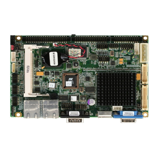
Page 16: Component Side
S u b C o m p a c t B o a r d G E N E - 5 3 1 5 2.2 Jumpers, Connectors, and Mechanical Drawings GENE-5315 Rev.A Component Side CN20 CN14 CN18 CN21 CN19 CN13... -
Page 17: Solder Side
S u b C o m p a c t B o a r d G E N E - 5 3 1 5 Solder Side 132.84 DIMM1 66.04 52.59 CFD1 12.43 0.00 2 - 4 Chapter 2 Quick Installation Guide... -
Page 18: Mechanical Drawings
S u b C o m p a c t B o a r d G E N E - 5 3 1 5 Mechanical Drawings HEATSINK HEIGHT (13.20) (12.55) (1.60) 137.16 133.93 133.93 132.27 132.56 131.95 125.81 125.56 123.73 120.27 119.27 108.27... - Page 19 S u b C o m p a c t B o a r d G E N E - 5 3 1 5 GENE-5315 Rev.B Component Side CN20 CN14 CN21 CN18 CN19 CN13 BAT1 CN16 CN15 2 - 6...
- Page 20 S u b C o m p a c t B o a r d G E N E - 5 3 1 5 Solder Side 132.84 DIMM1 66.04 52.53 CFD1 12.43 0.00 8.89 2 - 7 Chapter 2 Quick Installation Guide...
- Page 21 S u b C o m p a c t B o a r d G E N E - 5 3 1 5 Mechanical Drawings HEATSINK HEIGHT (13.20) (12.55) 137.16 133.93 133.93 132.22 131.95 125.56 125.75 123.73 120.27 114.94 106.60 96.71 92.07...
-
Page 22: List Of Jumpers
S u b C o m p a c t B o a r d G E N E - 5 3 1 5 2.3 List of Jumpers The board has a number of jumpers that allow you to configure your system to suit your application. -
Page 23: List Of Connectors
S u b C o m p a c t B o a r d G E N E - 5 3 1 5 2.4 List of Connectors The board has a number of connectors that allow you to configure your system to suit your application. The table below shows the function of each of the board’s connectors: Note: For further information about mating connectors, please refer to... - Page 24 S u b C o m p a c t B o a r d G E N E - 5 3 1 5 CN18 Mini-Din PS/2 CN19 Serial Port #1 CN20 CRT Display CN21 USB Port #3 and Port #4 CN22 LCD Inverter Voltage CN23...
-
Page 25: Setting Jumpers
S u b C o m p a c t B o a r d G E N E - 5 3 1 5 2.5 Setting Jumpers You configure your card to match the needs of your application by setting jumpers. A jumper is the simplest kind of electric switch. It consists of two metal pins and a small metal clip (often protected by a plastic cover) that slides over the pins to connect them. -
Page 26: At/Atx Power Type Selection (Jp1)
S u b C o m p a c t B o a r d G E N E - 5 3 1 5 2.6 AT/ATX Power Type Selection (JP1) Function ATX Power Supply AT Power Supply (Default) 2.7 CFD Master/Slave Selection (JP2) Function Slave Master (Default) -
Page 27: Com Ports Ri/+5V/+12V Selection (Jp5)
S u b C o m p a c t B o a r d G E N E - 5 3 1 5 2.10 COM Ports RI/+5V/+12V Selection (JP5) COM 1 Function +12V RI (Default) COM 2 Function +12V 9-10 11-12 RI (Default) -
Page 28: Floppy Connector (Cn2)
Active LED# Ground +5Volt. +5Volt. Ground N.C. Note: The IDE interface on GENE-5315 supports two IDE devices including CF card. If you use a CF card, GENE-5315 allows one IDE device. 2.14 Floppy Connector (CN2) Signal Signal Ground DENSEL# Ground N.C. -
Page 29: Parallel Port Connector (Cn3)
S u b C o m p a c t B o a r d G E N E - 5 3 1 5 Ground INDEX# Ground MTRA# Ground DRVB# Ground DRVA# Ground MTRB# Ground DIR# Ground STEP# Ground WDATA# Ground WGATE# Ground... -
Page 30: Front Panel Connector (Cn4)
S u b C o m p a c t B o a r d G E N E - 5 3 1 5 SLCT N.C. 2.16 Front Panel Connector (CN4) Signal Signal Power On Button (-) Power On Button (+) IDE LED (-) IDE LED (+) External Buzzer (-) -
Page 31: Audio Input/Output/Cdin/Mic (Cn7)
S u b C o m p a c t B o a r d G E N E - 5 3 1 5 DIO-2 CN6 Pin 2 Bit 6 U1 Pin 21 (GPIO 26) DIO-3 CN6 Pin 3 Bit 5 U1 Pin 22 (GPIO 25) DIO-4 CN6 Pin 4... -
Page 32: Power Socket (Cn9)
S u b C o m p a c t B o a r d G E N E - 5 3 1 5 +5 Volt. Standby 2.21 4P Power Socket (CN9) Signal +12 Volt. Ground Ground +5 Volt. 2.22 LVDS LCD Connector (CN10) Signal Signal N.C. -
Page 33: Pc/104 (Cn11) (For Rev.a Only)
S u b C o m p a c t B o a r d G E N E - 5 3 1 5 2.23 PC/104 (CN11) (For Rev. A only) J1/P1 IOCHCK* RSTDRV IRQ9 DRQ2 -12V ENDXFR* +12V IOCHRDY GND/KEY SMEMW* SMEMR*... - Page 34 MASTER* SD14 SD15 GND/KEY Note 1: GENE-5315 does not support PC/104 way legacy ISA-DMA mode caused by AMD architecture. Note 2: Allocation Method of PC/104 Card for GENE-5315 PC/104 connector on GENE-5315 cannot automatically get “Resource” when a new PC/104 card is added because of AMD...
-
Page 35: Ttl Lcd (Cn12)
S u b C o m p a c t B o a r d G E N E - 5 3 1 5 Geode’s architecture limitation. The following steps for setup the resources manually for your reference. Retrieve the resource of the PC/104 card. The information is typically contained in the manual of the PC/104 card. - Page 36 S u b C o m p a c t B o a r d G E N E - 5 3 1 5 Ground Ground Clock VSYNC HSYNC N.C. N.C. For 18-bit TFT LCD Signal Signal +5Volt. +5Volt. Ground Ground +3.3Volt.
-
Page 37: Serial Port #2 (Cn13)
S u b C o m p a c t B o a r d G E N E - 5 3 1 5 HSYNC N.C. N.C. 2.25 Serial Port #2 (CN13) COM2/ RS-232 Mode Signal Signal DCDB DTRB Ground DSRB RTSB CTSB... -
Page 38: Ethernet 10/100Base-Tx Rj-45 Phone Jack #1 (Cn15)
S u b C o m p a c t B o a r d G E N E - 5 3 1 5 +5 Volt. Ground 2.27 Ethernet 10/100 Base-TX RJ-45 Phone Jack #1 (CN15) Signal Signal RXD- RXD+ N.C. -
Page 39: Mini-Din Ps/2 Keyboard/Mouse Connector (Cn18)2-26
S u b C o m p a c t B o a r d G E N E - 5 3 1 5 Ground CIR_RX (Option) 2.30 Mini-DIN PS/2 Keyboard/ Mouse Connector (CN18) Signal Signal Keyboard Data Keyboard Data Ground Ground +5 Volt. -
Page 40: Usb Port #3 And Port #4 (Cn21)
S u b C o m p a c t B o a r d G E N E - 5 3 1 5 Ground 2.33 USB Port #3 and Port #4 (CN21) Signal Signal Ground Ground Ground Ground 2.34 LCD Inverter Voltage (CN22) Signal Backlight Control Ground... -
Page 41: Serial Port #5 (Cn24)(For Rev.b Only)
N.C. Note: An APM Mode limitation, OS (Operating System) recognizes serial port 5 & 6 of GENE-5315 Rev.B but is reverse. OS will reassign IRQ and give sequence of serial port 5 & 6 after uninstalling all of serial ports and second time boots in OS. -
Page 42: External Battery (Bat1)
G E N E - 5 3 1 5 Note: An APM Mode limitation, OS (Operating System) recognizes serial port 5 & 6 of GENE-5315 Rev.B but is reverse. OS will reassign IRQ and give sequence of serial port 5 & 6 after uninstalling all of serial ports and second time boots in OS. -
Page 43: Mini-Pci Slot (Mpci1)
S u b C o m p a c t B o a r d G E N E - 5 3 1 5 DACK# DASP# PDIAG# IO16# Ground Ground 2.41 Mini-PCI Slot (MPCI1) Standard Specification 2.42 DDR SODIMM Slot (DIMM1) Standard SODIMM Slot Note from AMD: Memory configurations supported. - Page 44 S u b C o m p a c t B o a r d G E N E - 5 3 1 5 Below Table for China RoHS Requirements 产品中有毒有害物质或元素名称及含量 AAEON Main Board/ Daughter Board/ Backplane 有毒有害物质或元素 部件名称 铅...
-
Page 45: Chapter 3 Award Bios Setup
S u b C o m p a c t B o a r d G E N E - 5 3 1 5 Chapter Award BIOS Setup Chapter 3 Award BIOS Setup 3-1... - Page 46 3. The CMOS memory has lost power and the configuration information has been erased. The GENE-5315 CMOS memory has an integral lithium battery backup for data retention. However, you will need to replace the complete unit when it finally runs down.
- Page 47 S u b C o m p a c t B o a r d G E N E - 5 3 1 5 3.2 Award BIOS Setup Awards BIOS ROM has a built-in Setup program that allows users to modify the basic system configuration. This type of information is stored in battery-backed CMOS RAM so that it retains the Setup information when the power is turned off.
- Page 48 S u b C o m p a c t B o a r d G E N E - 5 3 1 5 Advanced Chipset Features Use this menu to change the values in the chipset registers and optimize your system performance. Integrated Peripherals Use this menu to specify your settings for integrated peripherals.
- Page 49 Save CMOS value changes to CMOS and exit setup. Exit Without Saving Abandon all CMOS value changes and exit setup. You can refer to the “ AAEON BIOS Item Description.pdf” file in the CD for the meaning of each setting in this chapter.
-
Page 50: Chapter 4 Driver Installation
S u b C o m p a c t B o a r d G E N E - 5 3 1 5 Chapter Driver Installation 4 - 1 Chapter 4 Driver Installation... -
Page 51: Software Drivers
S u b C o m p a c t B o a r d G E N E - 5 3 1 5 4.1 Software Drivers This chapter describes the operation and installation of the display drivers supplied on the Supporting CD-ROM that are shipped with your product. -
Page 52: Necessary To Know
S u b C o m p a c t B o a r d G E N E - 5 3 1 5 4.2 Necessary to Know The instructions in this manual assume that you understand elementary concepts of MS-DOS and the IBM Personal Computer. Before you attempt to install any driver from the Supporting CD-ROM, you should: Know how to copy files from a CD-ROM to a directory on the... -
Page 53: Installing Vga Driver
S u b C o m p a c t B o a r d G E N E - 5 3 1 5 4.3 Installing VGA Driver Win XP / Win XPe VGA Place the Driver CD-ROM into your CD-ROM drive and follow the steps below to install. -
Page 54: Installing Aes Driver
S u b C o m p a c t B o a r d G E N E - 5 3 1 5 4.4 Installing AES Driver Win XP / Win XPe AES Place the Driver CD-ROM into your CD-ROM drive and follow the steps below to install. -
Page 55: Installing Pci To Isa Bridge Driver
S u b C o m p a c t B o a r d G E N E - 5 3 1 5 4.5 Installing PCI to ISA Bridge Driver (For Rev.A only) Win XP / Win XPe System Place the Driver CD-ROM into your CD-ROM drive and follow the following steps to install. -
Page 56: Installing Ethernet Driver
S u b C o m p a c t B o a r d G E N E - 5 3 1 5 4.6 Installing Ethernet Driver 1. Click on the Step 4 – Lan folder. 2. Double click on the Setup file located in the folder. 3. -
Page 57: Installing Audio Driver
S u b C o m p a c t B o a r d G E N E - 5 3 1 5 information. After you have made your selections and the configuration is what you want, press <ESC>. A prompt will appear asking if you want to save the configuration. - Page 58 S u b C o m p a c t B o a r d G E N E - 5 3 1 5 8. Click on Next. 9. Select Search for a suitable driver…, then click on Next. 10. Select Specify a location, then click on Next. 11.
-
Page 59: Appendix A Programming The Watchdog Timer
S u b C o m p a c t B o a r d G E N E - 5 3 1 5 Appendix Programming the Watchdog Timer A - 1 Appendix A Programming the Watchdog Timer... -
Page 60: Programming
S u b C o m p a c t B o a r d G E N E - 5 3 1 5 A.1 Programming GENE-5315 utilizes ITE 8712 chipset as its watchdog timer controller. ( K version ) Below are the procedures to complete its configuration and... - Page 61 S u b C o m p a c t B o a r d G E N E - 5 3 1 5 There are three steps to complete the configuration setup: (1) Enter the MB PnP Mode; (2) Modify the data of configuration registers;...
- Page 62 S u b C o m p a c t B o a r d G E N E - 5 3 1 5 Configure Control (Index=02h) This register is write only. Its values are not sticky; that is to say, a hardware reset will automatically clear the bits, and does not require the software to clear them.
-
Page 63: Ite8712 Watchdog Timer Initial Program
S u b C o m p a c t B o a r d G E N E - 5 3 1 5 WDT output through PWROK1/PWROK2 (pulse) enable note Select the interrupt level for WDT WatchDog Timer Time-out Value (LSB) Register (Index=73h, Default=00h) Description WDT Time-out value 7-0... - Page 64 S u b C o m p a c t B o a r d G E N E - 5 3 1 5 Watch_Dog_Setting: ;Timer setting mov al, cl mov cl, 73h call Superio_Set_Reg ;Clear by keyboard or mouse interrupt mov al, 0f0h mov cl, 71h call Superio_Set_Reg...
- Page 65 S u b C o m p a c t B o a r d G E N E - 5 3 1 5 MOV DX,02Eh MOV CX,04h Init_1: MOV AL,BYTE PTR CS:[SI] OUT DX,AL INC SI LOOP Init_1 Enter_Configuration_Mode ENDP Exit_Configuration_Mode PROC NEAR MOV AX,0202h CALL Write_Configuration_Data...
- Page 66 S u b C o m p a c t B o a r d G E N E - 5 3 1 5 CMP AL,12h JNE Not_Initial Need_Initial: Not_Initial: Check_Chip ENDP Read_Configuration_Data PROC NEAR MOV DX,WORD PTR CS:[Cfg_Port+04h] OUT DX,AL MOV DX,WORD PTR CS:[Cfg_Port+06h] IN AL,DX Read_Configuration_Data ENDP...
- Page 67 S u b C o m p a c t B o a r d G E N E - 5 3 1 5 Write_Configuration_Data ENDP Superio_Set_Reg proc near push ax MOV DX,WORD PTR CS:[Cfg_Port+04h] mov al,cl out dx,al pop ax inc dx out dx,al Superio_Set_Reg endp.Set_Logic_Device proc near...
- Page 68 S u b C o m p a c t B o a r d G E N E - 5 3 1 5 Cfg_Port DB 087h,001h,055h,055h DW 02Eh,02Fh END Main Note: Interrupt level mapping 0Fh-Dh: not valid 0Ch: IRQ12 03h: IRQ3 02h: not valid 01h: IRQ1...
-
Page 69: Appendix B I/O Information
S u b C o m p a c t B o a r d G E N E - 5 3 1 5 Appendix I/O Information B - 1 Appendix B I/O Information... -
Page 70: I/O Address Map
S u b C o m p a c t B o a r d G E N E - 5 3 1 5 B.1 I/O Address Map Address Description User Address 000-01F DMA Controller #1 000-000F 020-03F Interrupt Controller #1, Master 020-021 040-05F System Time... -
Page 71: Irq Mapping Chart For Rev.a
S u b C o m p a c t B o a r d G E N E - 5 3 1 5 B.3 IRQ Mapping Chart for Rev.A IRQ0 System Timer IRQ8 System CMOS / Real time clock IRQ1 Keyboard IRQ9 Microsoft ACPI –... - Page 72 S u b C o m p a c t B o a r d G E N E - 5 3 1 5 Appendix Mating Connector C - 1 Appendix C Mating Connector...
-
Page 73: C.1 List Of Mating Connectors And Cables
S u b C o m p a c t B o a r d G E N E - 5 3 1 5 C.1 List of Mating Connectors and Cables The table notes mating connectors and available cables. Connector Function Mating Connector Available... - Page 74 S u b C o m p a c t B o a r d G E N E - 5 3 1 5 CN14 System FAN Hobase 2503-H-3 Connector Technology CN15 Ethernet Neltron 7001-8P8C Connector CN16 Ethernet Neltron 7001-8P8C Connector CN17 IrDA...
Need help?
Do you have a question about the GENE-5315 and is the answer not in the manual?
Questions and answers