Table of Contents

Related Manuals for Aaeon GENE-QM77


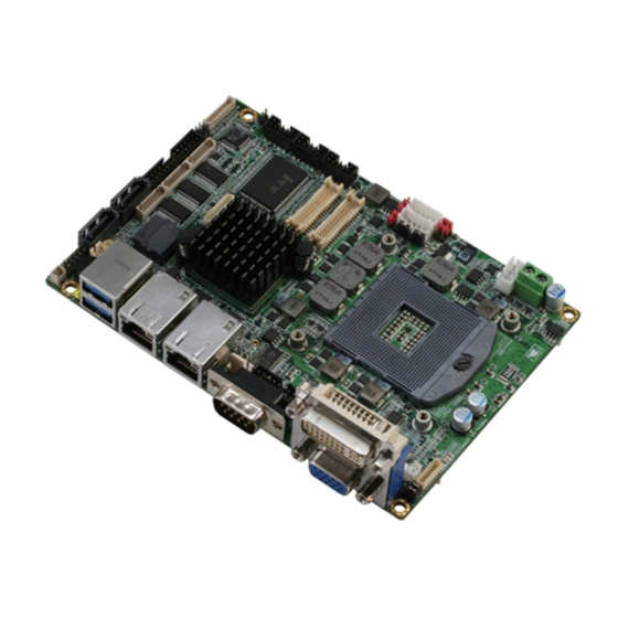
Summary of Contents for Aaeon GENE-QM77
- Page 1 GENE-QM77 Rev. A 3.5” Subcompact Board User’s Manual 4 Last Updated: April 12, 2016...
-
Page 2: Copyright Notice
AAEON assumes no liabilities resulting from errors or omissions in this document, or from the use of the information contained herein. AAEON reserves the right to make changes in the product design without notice to its users. - Page 3 Acknowledgement All other products’ name or trademarks are properties of their respective owners. Microsoft Windows is a registered trademark of Microsoft Corp. Intel, Pentium, Celeron, and Xeon are registered trademarks of Intel Corporation Core, Atom are trademarks of Intel Corporation ...
- Page 4 Packing List Before setting up your product, please make sure the following items have been shipped: Item Quantity GENE-QM77 Rev. A Cooler Product CD/DVD with User’s Manual (in pdf) and drivers If any of these items are missing or damaged, please contact your distributor or sales representative immediately.
- Page 5 (if any), its specifications, dimensions, jumper/connector settings/definitions, and driver installation instructions (if any), to facilitate users in setting up their product. Users may refer to the AAEON.com for the latest version of this document. Preface...
- Page 6 Safety Precautions Please read the following safety instructions carefully. It is advised that you keep this manual for future references All cautions and warnings on the device should be noted. Make sure the power source matches the power rating of the device. Position the power cord so that people cannot step on it.
- Page 7 If any of the following situations arises, please the contact our service personnel: Damaged power cord or plug Liquid intrusion to the device iii. Exposure to moisture Device is not working as expected or in a manner as described in this manual The device is dropped or damaged Any obvious signs of damage displayed on the device...
- Page 8 FCC Statement This device complies with Part 15 FCC Rules. Operation is subject to the following two conditions: (1) this device may not cause harmful interference, and (2) this device must accept any interference received including interference that may cause undesired operation.
- Page 9 China RoHS Requirements (CN) 产品中有毒有害物质或元素名称及含量 AAEON Main Board/ Daughter Board/ Backplane 有毒有害物质或元素 部件名称 铅 汞 镉 六价铬 多溴联苯 多溴二苯醚 (Pb) (Hg) (Cd) (Cr(VI)) (PBB) (PBDE) 印刷电路板 ○ ○ ○ ○ ○ ○ 及其电子组件 外部信号 ○ ○ ○ ○ ○ ○...
- Page 10 China RoHS Requirement (EN) Poisonous or Hazardous Substances or Elements in Products AAEON Main Board/ Daughter Board/ Backplane Poisonous or Hazardous Substances or Elements Hexavalent Polybrominated Polybrominated Component Lead Mercury Cadmium Chromium Biphenyls Diphenyl Ethers (Pb) (Hg) (Cd) (Cr(VI)) (PBB) (PBDE) PCB &...
-
Page 11: Table Of Contents
Table of Contents Chapter 1 - Product Specifications ..................1 Specifications ......................2 Chapter 2 – Hardware Information ..................5 Dimensions ....................... 6 Jumpers and Connectors ..................8 List of Jumpers ....................... 10 2.3.1 LVDS Port 2 Operating VDD Selection (JP2) ......11 2.3.2 LVDS Port 1 Backlight Inverter VCC Selection (JP3) .... - Page 12 2.4.7 LVDS Port 2 Inverter/ Backlight Connector (CN7) ....19 2.4.8 Audio I/O Port Connector (CN8) ..........19 2.4.9 LVDS Port 1 Connector (CN9) ............. 20 * LVDS1 LCD_PWR can be set to +3.3V or +5V by JP5........ 22 2.4.10 LVDS Port 2 Connector (CN10) ...........
- Page 13 System Test and Initialization ................46 AMI BIOS Setup ..................... 47 Chapter 4 – Drivers Installation .................... 48 Product CD/DVD ....................49 Appendix A - Watchdog Timer Programming ..............52 Watchdog Timer Registers .................. 53 ITE8728F Watchdog Timer Initial Program ............57 Appendix B - I/O Information ....................
-
Page 14: Chapter 1 - Product Specifications
Chapter 1 Chapter 1 - Product Specifications... -
Page 15: Specifications
Specifications System Form Factor 3.5” ® Processor Intel 3rd Generation Core™i7/i5 Mobile processor System Memory 204-pin DDR3 1066/1333/1600 MHz SODIMM x 1, up to 8GB I/O Chipset ITE IT8728F + Fintek F81216D ® Chipset Intel QM77/HM76 ... - Page 16 RS-232 x 3 RS-232/422/485 (auto flow) x 1 PS/2 Port Keyboard x 1, Mouse x 1 DI/O 8-bit Programmable Audio Line-in, Line-out, Mic-in *Note on OS For Linux, AAEON suggests the following: Chapter 1 – Product Specifications...
- Page 17 - Kernel 2.6.39 version or later: Set default BIOS/SATA operating mode to IDE - Use Ubuntu 12.04 version or later for better display performance Chapter 1 – Product Specifications...
-
Page 18: Chapter 2 - Hardware Information
Chapter 2 Chapter 2 – Hardware Information... -
Page 19: Dimensions
Dimensions Component side Chapter 2 – Hardware Information... - Page 20 Solder side Chapter 2 – Hardware Information...
-
Page 21: Jumpers And Connectors
Jumpers and Connectors Component side Component Side Chapter 2 – Hardware Information... -
Page 22: Solder Side
Solder side Solder Side Chapter 2 – Hardware Information... -
Page 23: List Of Jumpers
List of Jumpers Please refer to the table below for all of the board’s jumpers that you can configure for your application Label Function LVDS Port 2 Operating VDD Selection LVDS Port 1 Backlight Inverter VCC Selection LVDS Port 2 Backlight Inverter VCC Selection LVDS Port 1 Operating VDD Selection LVDS Port 1 Backlight Lightness Control Mode Selection LVDS Port 2 Backlight Lightness Control Mode Selection... -
Page 24: Lvds Port 2 Operating Vdd Selection (Jp2)
2.3.1 LVDS Port 2 Operating VDD Selection (JP2) 1 2 3 1 2 3 +3.3V (Default) 2.3.2 LVDS Port 1 Backlight Inverter VCC Selection (JP3) 1 2 3 1 2 3 +5V (Default) +12V 2.3.3 LVDS Port 2 Backlight Inverter VCC Selection (JP4) 1 2 3 1 2 3 +5V (Default) -
Page 25: Lvds Port 2 Backlight Lightness Control Mode Selection (Jp7)
2.3.6 LVDS Port 2 Backlight Lightness Control Mode Selection (JP7) 1 2 3 1 2 3 PWM Mode VR Mode (default) 2.3.7 COM2 Pin8 Function Selection (JP8) +12V Ring(Default) 2.3.8 Front Panel Connector (JP9) Signal PWR_BTN- PWR_BTN+ HDD_LED- HDD_LED+ SPEAKER- SPEAKER+ PWR_LED- PWR_LED+... -
Page 26: Touch Screen 4/5/8-Wire Selection (Jp10)
H/W RESET+ 2.3.9 Touch Screen 4/5/8-Wire Selection (JP10) 1 2 3 1 2 3 5-wire mode 4/8-wire mode (default) 2.3.10 Clear CMOS (JP11) 1 2 3 1 2 3 Clear CMOS Normal (default) 2.3.11 AT/ATX Power Supply Mode Selection (JP12) 1 2 3 1 2 3 ATX Mode... -
Page 27: List Of Connectors
List of Connectors Please refer to the table below for all of the board’s connectors that you can configure for your application Label Function LVDS Port 1 Inverter / Backlight Connector External +12V Input USB 2.0 Ports 7 and 8 USB 2.0 Ports 5 and 6 USB 2.0 Ports 3 and 4 External +5VSB Input... - Page 28 CN25 USB Ports 1 and 2 CN26 VGA / DVI Ports (depend on hardware configuration) CN27 COM Port 1 (D-SUB 9) CN28 CFast Slot CN29 DDR3 SODIMM Slot CN30 Mini Card Slot SATA1 SATA Port1 Connector SATA2 SATA Port 2 Connector Chapter 2 –...
-
Page 29: Lvds Port 1 Inverter/ Backlight Connector (Cn1)
2.4.1 LVDS Port 1 Inverter/ Backlight Connector (CN1) BLK_PWR BKL_CONTROL BKL_ENABLE Pin Name Signal Type Signal Level BKL_PWR +5V / +12V BKL_CONTROL BKL_ENABLE * LVDS1 BKL_PWR can be set to +5V or +12V by JP3. * LVDS1 BKL_CONTROL can be set by JP6. 2.4.2 External +12V Input (CN2) +12V GND Pin Name... -
Page 30: Usb2.0 Port 5 And Port 6 (Cn4)
+5VSB USB7_D- USB7_D+ USB8_D+ USB8_D- +5VSB * LVDS LCD_PWR can be set to 3.3V or +5V by JP1 * LVDS VDD power can be set by JP4 Pin Name Signal Type Signal Level +5VSB USB7_D- DIFF USB7_D+ DIFF USB8_D+ DIFF USB8_D- DIFF +5VSB... -
Page 31: Usb2.0 Port 3 And Port 4 (Cn5)
USB5_D+ DIFF USB6_D+ DIFF USB6_D- DIFF +5VSB 2.4.5 USB2.0 Port 3 and Port 4 (CN5) +5VSB USB3_D- USB3_D+ USB4_D+ USB4_D- +5VSB Pin Name Signal Type Signal Level +5VSB USB3_D- DIFF USB3_D+ DIFF USB4_D+ DIFF USB4_D- DIFF +5VSB 2.4.6 External +5VSB Input (CN6) Chapter 2 –... -
Page 32: Lvds Port 2 Inverter/ Backlight Connector (Cn7)
PS_ON# +5VSB Pin Name Signal Type Signal Level PS_ON# +3.3V +5VSB 2.4.7 LVDS Port 2 Inverter/ Backlight Connector (CN7) BLK_PWR BKL_CONTROL BKL_ENABLE Pin Name Signal Type Signal Level BKL_PWR +5V / +12V BKL_CONTROL BKL_ENABLE * LVDS2 BKL_PWR can be set to +5V or +12V by JP4. * LVDS2 BKL_CTL can be set by JP7. -
Page 33: Lvds Port 1 Connector (Cn9)
MIC_L MIC_R GND_AUDIO LINE_L_IN LINE_R_IN GND_AUDIO LEFT_OUT GND_AUDIO RIGHT_OUT +5V_AUDIO Pin Name Signal Type Signal Level MIC_L MIC_R GND_AUDIO LINE_L_IN LINE_R_IN GND_AUDIO LEFT_OUT GND_AUDIO RIGHT_OUT +5V_AUDIO 2.4.9 LVDS Port 1 Connector (CN9) PIN 29 PIN 30 PIN 1 PIN 2 Chapter 2 –... - Page 34 Pin Name Signal Type Signal Level BKL_ENABLE BKL_CONTROL LCD_PWR +3.3V/+5V LVDS_A_CLK- DIFF LVDS_A_CLK+ DIFF LCD_PWR +3.3V/+5V LVDS_DA0- DIFF LVDS_DA0+ DIFF LVDS_DA1- DIFF LVDS_DA1+ DIFF LVDS_DA2- DIFF LVDS_DA2+ DIFF LVDS_DA3- DIFF LVDS_DA3+ DIFF DDC_DATA +3.3V DDC_CLK +3.3V LVDS_DB0- DIFF LVDS_DB0+ DIFF LVDS_DB1- DIFF LVDS_DB1+...
-
Page 35: Lvds1 Lcd_Pwr Can Be Set To +3.3V Or +5V By Jp5
LCD_PWR +3.3V/+5V LVDS_B_CLK- DIFF LVDS_B_CLK+ DIFF * LVDS1 LCD_PWR can be set to +3.3V or +5V by JP5. 2.4.10 LVDS Port 2 Connector (CN10) PIN 29 PIN 30 PIN 1 PIN 2 Pin Name Signal Type Signal Level BKL_ENABLE BKL_CONTROL LCD_PWR +3.3V/+5V LVDS_A_CLK-... -
Page 36: Lvds2 Lcd_Pwr Can Be Set To +3.3V Or +5V By Jp2
LVDS_DA1+ DIFF LVDS_DA2- DIFF LVDS_DA2+ DIFF LVDS_DA3- DIFF LVDS_DA3+ DIFF DDC_DATA +3.3V DDC_CLK +3.3V LVDS_DB0- DIFF LVDS_DB0+ DIFF LVDS_DB1- DIFF LVDS_DB1+ DIFF LVDS_DB2- DIFF LVDS_DB2+ DIFF LVDS_DB3- DIFF LVDS_DB3+ DIFF LCD_PWR +3.3V/+5V LVDS_B_CLK- DIFF LVDS_B_CLK+ DIFF * LVDS2 LCD_PWR can be set to +3.3V or +5V by JP2. Chapter 2 –... -
Page 37: Com Port 2 Connector (Cn11)
2.4.11 COM Port 2 Connector (CN11) RS-232 Pin Name Signal Type Signal Level ± 9V ± 9V ± 9V RI/+5V/+12V IN/ PWR +5V/+12V RS-422 Pin Name Signal Type Signal Level RS422_TX- ± 5V RS422_RX+ RS422_TX+ ± 5V Chapter 2 – Hardware Information... -
Page 38: Lpt/ Digital I/O Port Connector (Cn12)
RS422_RX- NC/+5V/+12V +5V/+12V RS-485 Pin Name Signal Type Signal Level RS485_D- ± 5V RS485_D+ ± 5V NC/+5V/+12V +5V/+12V * COM2 RS-232/422/485 can be set by BIOS setting. Default is RS-232. * Pin 8 function can be set by JP8. 2.4.12 LPT/ Digital I/O Port Connector (CN12) LPT Mode DIO Mode... - Page 39 * LPT / Digital IO can be set by BIOS setting. Default is LPT Function LPT Mode Pin Name Signal Type Signal Level STROBE# AFD# ERROR# PRINT# SLIN# ACK# BUSY Chapter 2 – Hardware Information...
- Page 40 SLCT LPT Mode DIO Mode STROBE# AFD# ERROR# DIO0 PRINT# DIO1 SLIN# DIO2 DIO3 ACK# DIO7 BUSY DIO6 DIO5 SLCT DIO4 DIO Mode Pin Name Signal Type Signal Level DIO0 DIO1 DIO2 DIO3 Chapter 2 – Hardware Information...
-
Page 41: Com Port 3 Connector (Cn13)
DIO7 DIO6 DIO5 DIO4 GPIO Port # / Location I/O Port Pin Name (Pin #) Access Address Port 1/DIO0 Bit 0 of 0xA06 Port 2/DIO1 Bit 1 of 0xA06 Port 3/DIO2 Bit 2 of 0xA06 Port 4/DIO3 Bit 3 of 0xA06 Port 5/DIO4 Bit 0 of 0xA07 Port 6/DIO5... -
Page 42: Edp Connector (Cn29)
Pin Name Signal Type Signal Level ± 9V ± 9V ± 9V 2.4.14 eDP Connector (CN29) LAD0 LAD1 LAD2 LAD3 +3.3V LFRAME# LRESET# LCLK LDRQ0 LDRQ1 SERIRQ Pin Name Signal Type Signal Level Chapter 2 – Hardware Information... -
Page 43: Com Port 4 Connector (Cn15)
LAD0 +3.3V LAD1 +3.3V LAD2 +3.3V LAD3 +3.3V +3.3V +3.3V LFRAME# LRESET# +3.3V LCLK LDRQ0 LDRQ1 SERIRQ +3.3V 2.4.15 COM Port 4 Connector (CN15) Pin Name Signal Type Signal Level ± 9V ± 9V Chapter 2 – Hardware Information... -
Page 44: Uim Card Module (Cn16)
± 9V 2.4.16 UIM Card Module (CN16) UIM_PWR UIM_RST UIM_CLK UIM_VPP UIM_DATA Pin Name Signal Type Signal Level UIM_PWR UIM_RST UIM_CLK UIM_VPP UIM_DATA 2.4.17 PS/2 Keyboard/Mouse Combo Port Connector (CN17) KB_DATA KB_CLK +5VSB MS_CLK MS_DATA Pin Name Signal Type Signal Level KB_DATA KB_CLK Chapter 2 –... -
Page 45: 5Vsb Output W/Smbus (Cn18)
+5VSB MS_DATA MS_CLK 2.4.18 +5VSB Output w/SMBus (CN18) SMB_DATA SMB_CLK PS_ON# +5VSB Pin Name Signal Type Signal Level SMB_DATA +3.3V SMB_CLK +3.3V PS_ON# +3.3V +5VSB 2.4.19 Touch Screen Connector (CN19) 8 Wires 4 Wires 5 Wires TOP EXCITE UL(Y) BOTTOM EXCITE BOTTOM UR(H) LEFT EXCITE... - Page 46 * Touch mode can be set by JP10 4wire Pin Name Signal Type Signal Level TOP EXCITE BOTTOM EXCITE LEFT EXCITE RIGHT EXCITE TOP SENSE BOTTOM SENSE LEFT SENSE 4 Wires 5 Wires RIGHT SENSE UL(Y) BOTTOM UR(H) LEFT LL(L) RIGHT LR(X) SENSE(S)
-
Page 47: Cpu Fan Connector (Cn20)
8 Wires 4 Wires TOP EXCITE BOTTOM EXCITE BOTTOM LEFT EXCITE LEFT RIGHT EXCITE RIGHT TOP SENSE BOTTOM SENSE LEFT SENSE RIGHT SENSE 8-wire Pin Name Signal Type Signal Level TOP EXCITE BOTTOM EXCITE LEFT EXCITE RIGHT EXCITE TOP SENSE BOTTOM SENSE LEFT SENSE RIGHT SENSE... -
Page 48: Output For Sata Hdd (Cn22)
FAN_POWER FAN_TAC 2.4.21 +5V Output for SATA HDD (CN22) Pin Name Signal Type Signal Level 2.4.22 Realtek LAN (RJ-45) Port (CN23) ACT/LINK SPEED Pin Name Signal Type Signal Level MDI0+ DIFF MDI0- DIFF MDI1+ DIFF MDI2+ DIFF MDI2- DIFF MDI1- DIFF MDI3+ DIFF... -
Page 49: Intel Lan (Rj-45) Port (Cn24)
2.4.23 Intel LAN (RJ-45) Port (CN24) ACT/LINK SPEED Pin Name Signal Type Signal Level MDI0+ DIFF MDI0- DIFF MDI1+ DIFF MDI2+ DIFF MDI2- DIFF MDI1- DIFF MDI3+ DIFF MDI3- DIFF 2.4.24 USB Port 1 and Port 2 (CN25) Port 2 11 12 13 Port 1 2 3 4... -
Page 50: Vga / Dvi Ports (Cn26)
USB1_SSTX− DIFF USB1_SSTX+ DIFF +5VSB USB2_D- DIFF USB2_D+ DIFF USB2_SSRX− DIFF USB2_SSRX+ DIFF USB2_SSTX− DIFF USB2_SSTX+ DIFF 2.4.25 VGA / DVI Ports (CN26) C3 C4 Pin Name Signal Type Signal Level GREEN BLUE Chapter 2 – Hardware Information... - Page 51 RED_GND_RTN GREEN_GND_RTN BLUE_GND_RTN DDC_DATA HSYNC VSYNC DDC_CLK Pin Name Signal Type Signal Level TMDS_DAT2+ DIFF TMDS_DAT2- DIFF VGA_DDC_CLK VGA_DDC _DATA DVI_DDC_CLK DVI_DDC_DATA VSYNC TMDS_DAT1- DIFF TMDS_DAT1+ DIFF TMDS_DAT3- DIFF TMDS_DAT3+ DIFF Chapter 2 – Hardware Information...
-
Page 52: Com Port 1 (D-Sub 9) (Cn27)
HPLG_DETECT TMDS_DAT0- DIFF 2.4.26 COM Port 1 (D-SUB 9) (CN27) Pin Name Signal Type Signal Level ± 9V ± 9V ± 9V Chapter 2 – Hardware Information... -
Page 53: Cfast Slot (Cn28)
2.4.27 CFast Slot (CN28) Pin Name Signal Type Signal Level SATA_TX+ DIFF SATA_TX- DIFF SATA_RX- DIFF SATA_RX+ DIFF PC10 PC11 PC12 PC13 +3.3V +3.3V PC14 +3.3V +3.3V PC15 PC16 PC17 Chapter 2 – Hardware Information... -
Page 54: Ddr3 Sodimm Slot (Cn29)
2.4.28 DDR3 SODIMM Slot (CN29) Standard specification 2.4.29 MiniCard Slot (CN30) Pin Name Signal Type Signal Level PCIE_WAKE# +3.3VSB +3.3V +1.5V +1.5V PCIE_CLK_REQ# UIM_PWR UIM_DATA PCIE_REF_CLK- DIFF UIM_CLK PCIE_REF_CLK+ DIFF UIM_RST UIM_VPP W_DISABLE# +3.3V Chapter 2 – Hardware Information... - Page 55 PCIE_RST# +3.3V PCIE_RX- DIFF +3.3VSB +3.3V PCIE_RX+ DIFF +1.5V +1.5V SMB_CLK +3.3V PCIE_TX- DIFF SMB_DATA +3.3V PCIE_TX+ DIFF USB_D- DIFF USB_D+ DIFF +3.3VSB +3.3V +3.3VSB +3.3V +1.5V +1.5V Chapter 2 – Hardware Information...
-
Page 56: Sata Port 1 (Sata1)
+3.3VSB +3.3V 2.4.30 SATA Port 1 (SATA1) Pin 1 Pin 7 Pin Name Signal Type Signal Level SATA_TX+ DIFF SATA_TX- DIFF SATA_RX- DIFF SATA_RX+ DIFF 2.4.31 SATA Port 2 (SATA2) Pin 1 Pin 7 Pin Name Signal Type Signal Level SATA_TX+ DIFF SATA_TX-... - Page 57 SATA_RX- DIFF SATA_RX+ DIFF Chapter 2 – Hardware Information...
-
Page 58: Chapter 3 - Ami Bios Setup
Chapter 3 Chapter 3 - AMI BIOS Setup... -
Page 59: System Test And Initialization
System Test and Initialization The board uses certain routines to perform testing and initialization. If an error, fatal or non-fatal, is encountered, a few short beeps or an error message will be outputted. The board can usually continue the boot up sequence with non-fatal errors. The system configuration verification routines check the current system configuration against the values stored in the CMOS memory. -
Page 60: Ami Bios Setup
AMI BIOS Setup The AMI BIOS ROM has a pre-installed Setup program that allows users to modify basic system configurations, which is stored in the battery-backed CMOS RAM and BIOS NVRAM so that the information is retained when the power is turned off. To enter BIOS Setup, press <Del>... -
Page 61: Chapter 4 - Drivers Installation
Chapter 4 Chapter 4 – Drivers Installation... -
Page 62: Product Cd/Dvd
Product CD/DVD The GENE-QM77 Rev. A comes with a product DVD that contains all the drivers and utilities you need to setup your product. Insert the DVD and follow the steps in the autorun program to install the drivers. In case the program does not start, follow the sequence below to install the drivers. - Page 63 Step 4 – Install LAN Driver (Intel LAN chip) Click on the Step 4 – LAN (Intel) folder and select your OS Open the Setup.exe file in the folder Follow the instructions Drivers will be installed automatically Step 5 – Install Audio Driver Open the Step 5 - Audio folder and select your OS Open the.exe file in the folder Follow the instructions...
- Page 64 Drivers will be installed automatically Step 9 – Install Touch Driver Open the Step 9 – Touch folder and select your OS Open the Setup.exe file in the folder Follow the instructions Drivers will be installed automatically Step 10 – Install USB 3.0 Driver (Windows 7 only) Open the Step 10 –...
-
Page 65: Appendix A - Watchdog Timer Programming
Appendix A Appendix A - Watchdog Timer Programming... -
Page 66: A.1 Watchdog Timer Registers
A.1 Watchdog Timer Registers GENE-QM77 rev. A utilizes ITE IT8728F chipset as its watchdog timer controller. Below are the procedures to complete its configuration and the AAEON intial watchdog timer program is also attached based on which you can develop customized program to fit your application. - Page 67 (2) Modify the data of configuration registers; (3) Exit the MB PnP Mode. Undesired result may occur if the MB PnP Mode is not exited normally. (1) Enter the MB PnP Mode To enter the MB PnP Mode, four special I/O write operations are to be performed during Wait for Key state.
- Page 68 WatchDog Timer Configuration Registers Configure Control (Index=02h) This register is write only. Its values are not sticky; that is to say, a hardware reset will automatically clear the bits, and does not require the software to clear them. Appendix A – Watchdog Timer Programming...
- Page 69 WatchDog Timer Control Register (Index=71h, Default=00h) WatchDog Timer Configuration Register (Index=72h, Default=00h) WatchDog Timer Time-out Value Register (Index=73h, Default=00h) Appendix A – Watchdog Timer Programming...
-
Page 70: A.2 Ite8728F Watchdog Timer Initial Program
A.2 ITE8728F Watchdog Timer Initial Program .MODEL SMALL .CODE Main: CALL Enter_Configuration_mode CALL Check_Chip mov cl, 7 call Set_Logic_Device ;time setting mov cl, 10 ; 10 Sec dec al Watch_Dog_Setting: ;Timer setting mov al, cl mov cl, 73h call Superio_Set_Reg ;Clear by keyboard or mouse interrupt mov al, 0f0h mov cl, 71h... - Page 71 Initial_OK: CALL Exit_Configuration_mode MOV AH,4Ch INT 21h Enter_Configuration_Mode PROC NEAR MOV SI,WORD PTR CS:[Offset Cfg_Port] MOV DX,02Eh MOV CX,04h Init_1: MOV AL,BYTE PTR CS:[SI] OUT DX,AL INC SI LOOP Init_1 Enter_Configuration_Mode ENDP Exit_Configuration_Mode PROC NEAR MOV AX,0202h CALL Write_Configuration_Data Exit_Configuration_Mode ENDP Check_Chip PROC NEAR MOV AL,20h CALL Read_Configuration_Data...
- Page 72 CMP AL,87h JNE Not_Initial MOV AL,21h CALL Read_Configuration_Data CMP AL,12h JNE Not_Initial Need_Initial: Not_Initial: Check_Chip ENDP Read_Configuration_Data PROC NEAR MOV DX,WORD PTR CS:[Cfg_Port+04h] OUT DX,AL MOV DX,WORD PTR CS:[Cfg_Port+06h] IN AL,DX Read_Configuration_Data ENDP Write_Configuration_Data PROC NEAR MOV DX,WORD PTR CS:[Cfg_Port+04h] OUT DX,AL XCHG AL,AH MOV DX,WORD PTR CS:[Cfg_Port+06h]...
- Page 73 OUT DX,AL Write_Configuration_Data ENDP Superio_Set_Reg proc near push ax MOV DX,WORD PTR CS:[Cfg_Port+04h] mov al,cl out dx,al pop ax inc dx out dx,al Superio_Set_Reg endp.Set_Logic_Device proc near Set_Logic_Device proc near push ax push cx xchg al,cl mov cl,07h call Superio_Set_Reg pop cx pop ax Set_Logic_Device endp...
- Page 74 DW 02Eh,02Fh END Main Note: Interrupt level mapping 0Fh-Dh: not valid 0Ch: IRQ12 03h: IRQ3 02h: not valid 01h: IRQ1 00h: no interrupt selected Appendix A – Watchdog Timer Programming...
-
Page 75: Appendix B - I/O Information
Appendix B Appendix B - I/O Information... -
Page 76: I/O Address Map
I/O Address Map Appendix B – I/O Information... - Page 77 Appendix B – I/O Information...
-
Page 78: Memory Address Map
Memory Address Map Appendix B – I/O Information... -
Page 79: Irq Mapping Chart
IRQ Mapping Chart Appendix B – I/O Information... -
Page 80: Dma Channel Assignments
DMA Channel Assignments Appendix B – I/O Information... -
Page 81: Appendix C - Mating Connectors
Appendix C Appendix C – Mating Connectors... -
Page 82: List Of Mating Connectors And Cables
51021-0900 1701090150 Connector Cable LPT / Digital Parallel Port CN12 Molex 51110-2650 1701260200 IO Port Cable COM Port 3 Serial Port CN13 Molex 51021-0900 1701090150 Connector Cable SHR-12V-S- AAEON CN14 LPC Port 1703120130 LPC Cable Appendix C – Mating Connectors... - Page 83 COM Port 4 Serial Port CN15 Molex 51021-0900 1701090150 Connector Cable CN16 Molex 51021-0600 Connector P/S2 KB/MS P/S2 KB/MS CN17 PHDR-06VS 1700060152 Connector Cable External AUX Power CN18 PHR-6 PS_ON# Touch CN19 Screen SHR-9V-S-B Connector CPU Fan CN20 Molex 22-01-2035 Connector +5Vout 2 Pins For...
-
Page 84: Appendix D - Raid & Ahci Settings
Appendix D Appendix D – RAID & AHCI Settings... -
Page 85: Setting Raid
Setting RAID OS installation to SETUP RAID Mode Step 1: Extract the f6fly-x86.zip from “Driver CD -> Step7-RAID&AHCI\WinXP_32” and copy below files to diskette. Step 2: Connect the USB Floppy drive to the board and insert the diskette from previous step. Appendix D –... - Page 86 Step 3: Configure SATA Controller to RAID mode in BIOS SETUP Menu: Advanced -> SATA Configuration -> SATA Mode -> RAID Mode Step 4: Configure DVD/CD-ROM drive as the first boot device. Appendix D – RAID & AHCI Settings...
- Page 87 Step 5: Save changes and exit BIOS SETUP Step 6: Press CTRL-I to enter RAID Configuration Utility Appendix D – RAID & AHCI Settings...
- Page 88 Step 7: Choose “1. Create RAID Volume” Step 8 – Configure RAID parameters for the system Appendix D – RAID & AHCI Settings...
- Page 89 Step 9 – Choose “Create Volume” and confirmed in next warning message. Appendix D – RAID & AHCI Settings...
- Page 90 Step 10 – Exit RAID Configuration Utility and Reboot to DVD/CD-ROM device to install Step 11 – Press “F6” to install RAID driver Step 12 – Press “S” to install RAID driver Appendix D – RAID & AHCI Settings...
- Page 91 Step 13 – Choose “Intel(R) Mobile Express Chipset SATA RAID Controller” Step 14 – It will show the model you selected and then press ”ENTER”. Windows Setup will continue to install OS. Appendix D – RAID & AHCI Settings...
-
Page 92: Setting Ahci
Setting AHCI OS installation to SETUP AHCI Mode Step 1: Extract the f6fly-x86.zip from “Driver CD -> Step7 - RAID&AHCI\WinXP_32” and copy below files to diskette. Step 2: Connect the USB Floppy drive to the board and insert the diskette from previous step. - Page 93 Step 3: Configure SATA Controller to RAID mode in BIOS SETUP Menu: Advanced -> SATA Configuration -> SATA Mode -> AHCI Mode Step 4: Configure DVD/CD-ROM drive as the first boot device. Appendix D – RAID & AHCI Settings...
- Page 94 Step 5: Save changes and exit BIOS SETUP Step 6 – Boot to DVD/CD-ROM device to install OS Step 7 – Press “F6” to install AHCI driver Appendix D – RAID & AHCI Settings...
- Page 95 Step 8 – Press “S” to install AHCI driver Step 9 – Choose “Intel(R) 7 Series Chipset Family SATA AHCI Controller” Appendix D – RAID & AHCI Settings...
- Page 96 Step 10 – It will show the model you selected and then press ”ENTER”. Windows Setup will continue to install OS. Appendix D – RAID & AHCI Settings...
-
Page 97: Appendix E - Electrical Specifications For I/O Ports
Appendix E Appendix E – Electrical Specifications for I/O Ports... -
Page 98: Electrical Specifications For I/O Ports
Electrical Specifications for I/O Ports Reference Signal Name Rate Output LVDS Port 1 Inverter +5V/2A or / Backlight +12V/2A Connector LVDS Port 2 Inverter +5V/2A or / Backlight +12V/2A Connector USB 2.0 Ports 7 and USB 2.0 Ports 5 and +5V/0.5A (per channel) USB 2.0 Ports 3 and... - Page 99 CPU FAN CN20 +12V/0.5A +5V Output for CN22 +5V/1A SATA HDD VGA / DVI Ports (depend on VGA: +5V +5V/1A (reserved) CN26 hardware DVI : +5V +5V/0.5A configuration) CFast Slot CN28 +3.3V +3.3V/0.5A +3.3VSB +3.3V/1.1A Mini Card Slot CN30 +1.5V +1.5V/0.375A LPC Port CN14...
Need help?
Do you have a question about the GENE-QM77 and is the answer not in the manual?
Questions and answers