Table of Contents
Advertisement
Quick Links
Download this manual
See also:
Manual
Advertisement
Table of Contents

Subscribe to Our Youtube Channel
Related Manuals for Aaeon GENE-9455 Rev.B


Summary of Contents for Aaeon GENE-9455 Rev.B
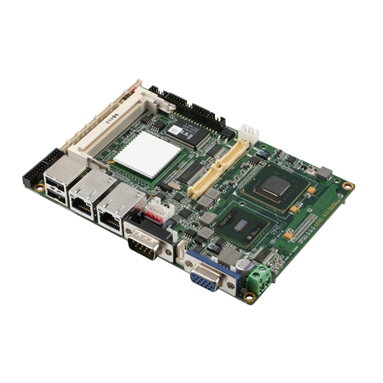
- Page 1 S u b C o m p a c t B o a r d G E N E - 9 4 5 5 R e v . B GENE-9455 Rev.B ® Intel Atom N270 Processor With LVDS, Ethernet, 1 Mini PCI, 1 Mini Card, 6 USB2.0, 4 COM, 1 Parallel...
-
Page 2: Copyright Notice
AAEON assumes no liabilities resulting from errors or omissions in this document, or from the use of the information contained herein. AAEON reserves the right to make changes in the product design without notice to its users. - Page 3 S u b C o m p a c t B o a r d G E N E - 9 4 5 5 R e v . B Acknowledgments All other products’ name or trademarks are properties of their respective owners.
-
Page 4: Packing List
G E N E - 9 4 5 5 R e v . B Packing List Before you begin installing your card, please make sure that the following materials have been shipped: • GENE-9455 Rev.B CPU Card • Quick Installation Guide • CD-ROM for manual (in PDF format) and drivers •... -
Page 5: Table Of Contents
S u b C o m p a c t B o a r d G E N E - 9 4 5 5 R e v . B Contents Chapter 1 General Information 1.1 Introduction..............1-2 1.2 Features ..............1-3 1.3 Specifications ............ - Page 6 S u b C o m p a c t B o a r d G E N E - 9 4 5 5 R e v . B 2.18 2 LVDS Connector for 18/24-bit LCD (CN7) ..2-15 2.19 Onboard BIOS Programming I/F(CN8)(Optional) ... 2-15 2.20 COM Port 4 Connector (CN9) .........
- Page 7 S u b C o m p a c t B o a r d G E N E - 9 4 5 5 R e v . B 2.42 Mini-Card Slot (CN32) ..........2-22 2.43 CompactFlash Disk (CFD1) ........2-23 2.44 Mini-PCI Slot (MPC1) ..........
-
Page 8: Chapter 1 General Information
S u b C o m p a c t B o a r d G E N E - 9 4 5 5 R e v . B Chapter General Information 1- 1 Chapter 1 General Information... -
Page 9: Introduction
RS-232/422/485 and 8-bit digital I/O are configured on the GENE-9455 Rev.B as well. Full functions make GENE-9455 Rev.B user friendly. With the GENE-9455 Rev.B, there are no more worries about installing many necessary devices to complete the functions of your system. -
Page 10: Features
S u b C o m p a c t B o a r d G E N E - 9 4 5 5 R e v . B 1.2 Features ® Onboard Intel Atom™ N270 Processor ® Intel 945GSE + ICH7M SODIMM DDR2 400/533, Max. -
Page 11: Specifications
S u b C o m p a c t B o a r d G E N E - 9 4 5 5 R e v . B 1.3 Specifications System ® Processor Intel Atom™ N270 processor up to 1.6 GHz with FSB 533 System Memory 200-pin SODIMM DDR2 400/533 x 1, Max. - Page 12 S u b C o m p a c t B o a r d G E N E - 9 4 5 5 R e v . B ® Power Consumption Intel Atom™ N270, DDRII 667 2GB, 1.55A @ +12V Board Size 5.75”(L) x 4”(W) (146mm x 101.6mm)
- Page 13 S u b C o m p a c t B o a r d G E N E - 9 4 5 5 R e v . B Storage SATA 1 x 1, Type 2 CompactFlash™ x 1 Serial Port RS-232 x 3, RS-232/422/485 x 1 Parallel Port SPP/EPP/ECP x 1...
-
Page 14: Chapter 2 Quick Installation Guide
S u b C o m p a c t B o a r d G E N E - 9 4 5 5 R e v . B Chapter Quick Installation Guide Notice: The Quick Installation Guide is derived from Chapter 2 of user manual. -
Page 15: Safety Precautions
S u b C o m p a c t B o a r d G E N E - 9 4 5 5 R e v . B 2.1 Safety Precautions Always completely disconnect the power cord from your board whenever you are working on it. -
Page 16: Location Of Connectors And Jumpers
S u b C o m p a c t B o a r d G E N E - 9 4 5 5 R e v . B 2.2 Location of Connectors and Jumpers Component Side CN25 CN30 CN28 CN31 CN27 CN20... -
Page 17: Solder Side
S u b C o m p a c t B o a r d G E N E - 9 4 5 5 R e v . B Solder Side DIMM1 CFD1 Chapter 2 Quick Installation Guide... -
Page 18: Mechanical Drawing
S u b C o m p a c t B o a r d G E N E - 9 4 5 5 R e v . B 2.3 Mechanical Drawing Component Side (12.55) (6.50) 146.05 142.85 142.87 142.82 136.14 121.92 117.81... - Page 19 S u b C o m p a c t B o a r d G E N E - 9 4 5 5 R e v . B Solder Side 139.90 65.94 25.76 11.94 0.00 Chapter 2 Quick Installation Guide...
-
Page 20: List Of Jumpers
S u b C o m p a c t B o a r d G E N E - 9 4 5 5 R e v . B 2.4 List of Jumpers The board has a number of jumpers that allow you to configure your system to suit your application. -
Page 21: List Of Connectors
S u b C o m p a c t B o a r d G E N E - 9 4 5 5 R e v . B 2.5 List of Connectors The board has a number of connectors that allow you to configure your system to suit your application. - Page 22 S u b C o m p a c t B o a r d G E N E - 9 4 5 5 R e v . B CN20 SATA 1 Connector CN21 +12V Power Input Connector CN22 RJ-45 Ethernet#1 Connector CN23 RJ-45 Ethernet#2 Connector CN24...
-
Page 23: Setting Jumpers
S u b C o m p a c t B o a r d G E N E - 9 4 5 5 R e v . B 2.6 Setting Jumpers You configure your card to match the needs of your application by setting jumpers. -
Page 24: Com2 Ring/+5V/+12V Selection (Jp1)
S u b C o m p a c t B o a r d G E N E - 9 4 5 5 R e v . B 2.7 COM2 Ring/+5V/+12V Selection (JP1) Function +12V RI (Default) 2.8 Clear CMOS (JP2) Function Normal (Default) Clear CMOS... -
Page 25: External +5V Standby Power Input & Ps On# (Cn1)
S u b C o m p a c t B o a r d G E N E - 9 4 5 5 R e v . B 2.12 External +5V Standby Power Input & PS ON# (CN1) Signal PS_ON# Ground +5 Volt. -
Page 26: Parallel Port Connector (Cn3)
S u b C o m p a c t B o a r d G E N E - 9 4 5 5 R e v . B 2.14 Parallel Port Connector (CN3) Name Name AFD# ERROR# PINIT# SLIN# Ground Ground Ground... -
Page 27: Com Port 3 Connector (Cn6)
S u b C o m p a c t B o a r d G E N E - 9 4 5 5 R e v . B CTSB DTRB RIB / +5 Volt. / +12 Volt. Ground COM2 RS-422 mode Signal Signal TXD-... -
Page 28: Nd Lvds Connector For 18/24-Bit Lcd (Cn7)
S u b C o m p a c t B o a r d G E N E - 9 4 5 5 R e v . B 2.18 2nd LVDS Connector for 18/24-bit LCD (CN7) Signal Signal Back-Light Enable LCD Volt. -
Page 29: Com Port 4 Connector (Cn9)
S u b C o m p a c t B o a r d G E N E - 9 4 5 5 R e v . B 2.20 COM Port 4 Connector (CN9) Signal Signal DCDD DSRD RTSD CTSD DTRD Ground... -
Page 30: Usb Port 2 Connector (Cn13)
S u b C o m p a c t B o a r d G E N E - 9 4 5 5 R e v . B LCD Volt. Ground LA_DATA#_0 LA_DATA_0 LA_DATA#_1 LA_DATA_1 LA_DATA#_2 LA_DATA_2 LB_DATA#_0 LB_DATA_0 LB_DATA#_1 LB_DATA_1 LB_DATA#_2... -
Page 31: Usb Port 4 Connector (Cn15)
S u b C o m p a c t B o a r d G E N E - 9 4 5 5 R e v . B 2.26 USB Port 4 Connector (CN15) Signal +5 Volt. Standby Data- Data+ Ground Ground... -
Page 32: Keyboard/Mouse Connector (Cn19)
S u b C o m p a c t B o a r d G E N E - 9 4 5 5 R e v . B Ground Ground Backlight Enable (Controlled by i82945GSE) 2.30 Keyboard/Mouse Connector (CN19) Signal Signal Keyboard Data... -
Page 33: Ethernet #2 Connector (Cn23)
S u b C o m p a c t B o a r d G E N E - 9 4 5 5 R e v . B MDI1_1+ / RXD+ MDI1_1- / RXD- TCD1_0 TCD1_1 MDI1_2+ MDI1_2- MDI1_3+ MDI1_3- SPD100_1_LED SPD1K_1_LED... -
Page 34: Audio Inp/Out Cd In And Mic Connector (Cn26)
S u b C o m p a c t B o a r d G E N E - 9 4 5 5 R e v . B SMBCLK Ground PS_ON# +5 Volt. Standby 2.37 Audio In/Out/ CD In and MIC Connector (CN26) Signal Signal MIC_Vcc... -
Page 35: Crt Display Connector (Cn30)
S u b C o m p a c t B o a r d G E N E - 9 4 5 5 R e v . B 2.40 CRT Display Connector (CN30) Signal Signal GREEN BLUE GREEN Ground Ground Ground +5 Volt. -
Page 36: Compactflash Disk (Cfd1)
S u b C o m p a c t B o a r d G E N E - 9 4 5 5 R e v . B PCIE_CLK UIM_RESET Ground UIM_VPP Ground W_DISABLE# Ground PCIE_RST# PCIE_RXN +3.3 Volt. Standby PCIE_RXP Ground Ground... -
Page 37: Mini-Pci Slot (Mpc1)
S u b C o m p a c t B o a r d G E N E - 9 4 5 5 R e v . B PDD7 PDD15 PDCS#1 PDCS#3 Ground Ground Ground PDIOR# Ground PDIOW# Ground +3.3 Volt. - Page 38 S u b C o m p a c t B o a r d G E N E - 9 4 5 5 R e v . B Below Table for China RoHS Requirements 产品中有毒有害物质或元素名称及含量 AAEON Main Board/ Daughter Board/ Backplane 有毒有害物质或元素 部件名称 铅...
-
Page 39: Chapter 3 Award Bios Setup
S u b C o m p a c t B o a r d G E N E - 9 4 5 5 R e v . B Chapter Award BIOS Setup Chapter 3 Award BIOS Setup 3-1... -
Page 40: System Test And Initialization
3. The CMOS memory has lost power and the configuration information has been erased. The GENE-9455 Rev.B CMOS memory has an integral lithium battery backup for data retention. However, you will need to replace the complete unit when it finally runs down. -
Page 41: Award Bios Setup
S u b C o m p a c t B o a r d G E N E - 9 4 5 5 R e v . B 3.2 Award BIOS Setup Awards BIOS ROM has a built-in Setup program that allows users to modify the basic system configuration. - Page 42 Exit Without Saving Abandon all CMOS value changes and exit setup. You can refer to the “ AAEON BIOS Item Description.pdf” file in the CD for the meaning of each setting in this chapter. Chapter 3 Award BIOS Setup 3-4...
-
Page 43: Chapter 4 Driver Installation
S u b C o m p a c t B o a r d G E N E - 9 4 5 5 R e v . B Chapter Driver Installation Chapter 4 Driver Installation... - Page 44 S u b C o m p a c t B o a r d G E N E - 9 4 5 5 R e v . B The GENE-9455 Rev.B comes with a CD-ROM that contains all drivers and utilities that meet your needs.
- Page 45 G E N E - 9 4 5 5 R e v . B 4.1 Installation: Insert the GENE-9455 Rev.B CD-ROM into the CD-ROM Drive. And install the drivers from Step 1 to Step 5 in order. Step 1 – Install INF Driver 1.
- Page 46 S u b C o m p a c t B o a r d G E N E - 9 4 5 5 R e v . B Step 4 – Install Audio Driver 1. Click on the Step 4 - Realtek ALC655 Audio Driver folder and select the OS folder your system is 2.
-
Page 47: Appendix A Programming The Watchdog Timer
S u b C o m p a c t B o a r d G E N E - 9 4 5 5 R e v . B Appendix Programming the Watchdog Timer Appendix A Programming the Watchdog Timer A-1... -
Page 48: Programming
G E N E - 9 4 5 5 R e v . B A.1 Programming GENE-9455 Rev.B utilizes ITE 8781 chipset as its watchdog timer controller. Below are the procedures to complete its configuration and the AAEON initial watchdog timer program is also attached based on which you can develop customized program to fit your application. - Page 49 S u b C o m p a c t B o a r d G E N E - 9 4 5 5 R e v . B There are three steps to complete the configuration setup: (1) Enter the MB PnP Mode;...
- Page 50 S u b C o m p a c t B o a r d G E N E - 9 4 5 5 R e v . B WatchDog Timer Configuration Registers Configure Control (Index=02h) This register is write only. Its values are not sticky; that is to say, a hardware reset will automatically clear the bits, and does not require the software to clear them.
- Page 51 S u b C o m p a c t B o a r d G E N E - 9 4 5 5 R e v . B Watch Dog Timer 1, 2, 3 Configuration Register (Index=72h, 82h, 92h Default=001s0000b) Watch Dog Timer 1,2,3 Time-Out Value (LSB) Register (Index=73h,83h,93h, Default=38h) Watch Dog Timer 1,2,3 Time-Out Value (MSB) Register...
-
Page 52: Ite8781 Watchdog Timer Initial Program
S u b C o m p a c t B o a r d G E N E - 9 4 5 5 R e v . B A.2 ITE8781 Watchdog Timer Initial Program .MODEL SMALL .CODE Main: CALL Enter_Configuration_mode CALL Check_Chip mov cl, 7 call Set_Logic_Device... - Page 53 S u b C o m p a c t B o a r d G E N E - 9 4 5 5 R e v . B call Superio_Set_Reg ; game port enable mov cl, 9 call Set_Logic_Device Initial_OK: CALL Exit_Configuration_mode MOV AH,4Ch...
- Page 54 S u b C o m p a c t B o a r d G E N E - 9 4 5 5 R e v . B CALL Write_Configuration_Data Exit_Configuration_Mode ENDP Check_Chip PROC NEAR MOV AL,20h CALL Read_Configuration_Data CMP AL,87h JNE Not_Initial MOV AL,21h...
- Page 55 S u b C o m p a c t B o a r d G E N E - 9 4 5 5 R e v . B OUT DX,AL MOV DX,WORD PTR CS:[Cfg_Port+06h] IN AL,DX Read_Configuration_Data ENDP Write_Configuration_Data PROC NEAR MOV DX,WORD PTR CS:[Cfg_Port+04h] OUT DX,AL XCHG AL,AH...
- Page 56 S u b C o m p a c t B o a r d G E N E - 9 4 5 5 R e v . B Set_Logic_Device proc near push ax push cx xchg al,cl mov cl,07h call Superio_Set_Reg pop cx pop ax...
-
Page 57: Appendix B I/O Information
S u b C o m p a c t B o a r d G E N E - 9 4 5 5 R e v . B Appendix I/O Information B - 1 Appendix B I/O Information... -
Page 58: I/O Address Map
S u b C o m p a c t B o a r d G E N E - 9 4 5 5 R e v . B B.1 I/O Address Map B - 2 Appendix B I/O Information... -
Page 59: St Mb Memory Address Map
S u b C o m p a c t B o a r d G E N E - 9 4 5 5 R e v . B B.2 1 MB Memory Address Map B - 3 Appendix B I/O Information... -
Page 60: Irq Mapping Chart
S u b C o m p a c t B o a r d G E N E - 9 4 5 5 R e v . B B.3 IRQ Mapping Chart B.4 DMA Channel Assignments B - 4 Appendix B I/O Information... -
Page 61: Appendix C Mating Connector
S u b C o m p a c t B o a r d G E N E - 9 4 5 5 R e v . B Appendix Mating Connecotor C - 1 Appendix C Mating Connector... -
Page 62: List Of Mating Connectors And Cables
S u b C o m p a c t B o a r d G E N E - 9 4 5 5 R e v . B C.1 List of Mating Connectors and Cables The table notes mating connectors and available cables. Mating Connector Connector Available... - Page 63 S u b C o m p a c t B o a r d G E N E - 9 4 5 5 R e v . B Cable LVDS Invertor CN16 Inverter Molex ZHR-5 1705050153 Cable Connector LVDS Invertor CN18 Inverter...
Need help?
Do you have a question about the GENE-9455 Rev.B and is the answer not in the manual?
Questions and answers