Table of Contents
Advertisement
Quick Links
Advertisement
Table of Contents

Related Manuals for Aaeon GENE-LN05


Summary of Contents for Aaeon GENE-LN05
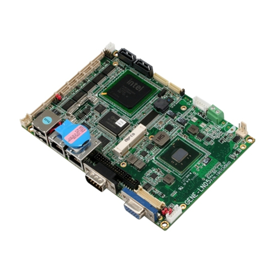
- Page 1 G E N E - L N 0 5 R e v . B GENE-LN05 Rev.B ® Intel Atom™N455/D525 Processors ® Intel 82567V & 82583V for 10/100/1000Mbps 2 SATA 3.0 Gb/s, 1 CompactFlash™ 6 COM, 7 USB2.0, Digital I/O 1 Mini Card/ SMBus/ LPC GENE-LN05 Rev.B Manual 4 July 17, 2015...
- Page 2 AAEON assumes no liabilities resulting from errors or omissions in this document, or from the use of the information contained herein. AAEON reserves the right to make changes in the product design without notice to its users.
- Page 3 S u b C o m p a c t B o a r d G E N E - L N 0 5 R e v . B Acknowledgments All other products’ name or trademarks are properties of their respective owners.
- Page 4 • CD-ROM for manual (in PDF format) and drivers • GENE-LN05 Rev.B with Active Cooler (D525 Version) or with Passive Cooler (N455 Version) If any of these items should be missing or damaged, please contact your distributor or sales representative immediately.
-
Page 5: Table Of Contents
S u b C o m p a c t B o a r d G E N E - L N 0 5 R e v . B Contents Chapter 1 General Information 1.1 Introduction ..............1-2 1.2 Features ..............1-3 1.3 Specifications ............ - Page 6 S u b C o m p a c t B o a r d G E N E - L N 0 5 R e v . B 2.18 SATA Port #2 (CN5) ..........2-13 2.19 SATA Port #1 (CN6) ..........2-13 2.20 LPC Expansion I/F (CN7) ........
- Page 7 S u b C o m p a c t B o a r d G E N E - L N 0 5 R e v . B 2.41 LVDS Inverter Connector (CN28) ......2-22 2.42 LVDS Output (CN29)..........2-22 2.43 USB Port 1 &...
- Page 8 S u b C o m p a c t B o a r d G E N E - L N 0 5 R e v . B Appendix C Mating Connector C.1 List of Mating Connectors and Cables....C-2...
-
Page 9: Chapter 1 General Information
S u b C o m p a c t B o a r d G E N E - L N 0 5 R e v . B Chapter General Information 1- 1 Chapter 1 General Information... -
Page 10: Introduction
Moreover, two SATA 3.0 Gb/s (optional RAID 0 &1) and one Type2 CompactFlash storage is configured on the GENE-LN05 Rev.B. In addition to the diverse storages, GENE-LN05 Rev.B also equips seven USB2.0, six COM, one parallel, and one keyboard/mouse ports for flexible I/O expansions. There are no more worries about installing many necessary devices to complete the functions of your system. -
Page 11: Features
S u b C o m p a c t B o a r d G E N E - L N 0 5 R e v . B 1.2 Features ® Intel Atom™ N455/D525 Processors Up To 1.8 GHz ®... -
Page 12: Specifications
S u b C o m p a c t B o a r d G E N E - L N 0 5 R e v . B 1.3 Specifications System ® Processor Intel Atom™ N455/D525 1.8GHz Processors ... - Page 13 S u b C o m p a c t B o a r d G E N E - L N 0 5 R e v . B Board Size 5.75”(L) x 4”(W) (146mm x 101.6mm) Gross Weight 0.88 lb (0.4 kg) ...
- Page 14 S u b C o m p a c t B o a r d G E N E - L N 0 5 R e v . B RS-232/422/485 (auto flow) x 1 (AAEON recommends for the Serial Port to be at the 9600 baud rate during high temperature operation.)
- Page 15 S u b C o m p a c t B o a r d G E N E - L N 0 5 R e v . B side of a SODIMM is populated, the other side is either identical or empty. Supported DDR3 SODIMM module configurations.
-
Page 16: Chapter 2 Quick Installation Guide
S u b C o m p a c t B o a r d G E N E - L N 0 5 R e v . B Chapter Quick Installation Guide Chapter 2 Quick Installation Guide... -
Page 17: Safety Precautions
S u b C o m p a c t B o a r d G E N E - L N 0 5 R e v . B 2.1 Safety Precautions Always completely disconnect the power cord from your board whenever you are working on it. -
Page 18: Location Of Connectors & Jumpers
S u b C o m p a c t B o a r d G E N E - L N 0 5 R e v . B 2.2 Location of Connectors and Jumpers Component Side Chapter 2 Quick Installation Guide... - Page 19 S u b C o m p a c t B o a r d G E N E - L N 0 5 R e v . B Solder Side Chapter 2 Quick Installation Guide...
-
Page 20: Mechanical Drawing
S u b C o m p a c t B o a r d G E N E - L N 0 5 R e v . B 2.3 Mechanical Drawing Component Side Chapter 2 Quick Installation Guide... - Page 21 S u b C o m p a c t B o a r d G E N E - L N 0 5 R e v . B Solder Side Chapter 2 Quick Installation Guide...
-
Page 22: List Of Jumpers
S u b C o m p a c t B o a r d G E N E - L N 0 5 R e v . B 2.4 List of Jumpers The board has a number of jumpers that allow you to configure your system to suit your application. -
Page 23: List Of Connectors
S u b C o m p a c t B o a r d G E N E - L N 0 5 R e v . B 2.5 List of Connectors The board has a number of connectors that allow you to configure your system to suit your application. - Page 24 S u b C o m p a c t B o a r d G E N E - L N 0 5 R e v . B CN21 COM Port #3 CN22 COM Port #2 CN23 Audio Line-In/Out and MIC Connector CN24 RJ-45 Ethernet #2 CN25...
-
Page 25: Setting Jumpers
S u b C o m p a c t B o a r d G E N E - L N 0 5 R e v . B 2.6 Setting Jumpers You configure your card to match the needs of your application by setting jumpers. -
Page 26: Touch Screen 4/5/8-Wire Mode Selection (Jp1)
S u b C o m p a c t B o a r d G E N E - L N 0 5 R e v . B 2.7 Touch Screen 4/5/8-wire Mode Selection (JP1) Function 1-2 Closed 4/8-wire (Default) 1-2 Open 5-wire 2.8 Auto Power Button Selection (JP2) -
Page 27: Lvds Operating Voltage Selection (Jp6)
S u b C o m p a c t B o a r d G E N E - L N 0 5 R e v . B 2.12 LVDS Operating Voltage Selection (JP6) Function +3.3V (Default) 2.13 LVDS Inverter Voltage Selection (JP7) Function +12V +5V (Default) -
Page 28: External +5Vsb Input (Cn4)
S u b C o m p a c t B o a r d G E N E - L N 0 5 R e v . B PSON# +5 Volt. Standby 2.17 External +5VSB Input (CN4) Signal PSON# Ground +5V Standby 2.18 SATA Port # 2 (CN5) -
Page 29: Lpc Expansion I/F (Cn7)
S u b C o m p a c t B o a r d G E N E - L N 0 5 R e v . B 2.20 LPC Expansion I/F (CN7) Signal LAD0 LAD1 LAD2 LAD3 +3.3 Volt. LFRAME# LRESET# Ground... -
Page 30: Touch Screen Connector (Cn10)
S u b C o m p a c t B o a r d G E N E - L N 0 5 R e v . B 2.23 Touch Screen Connector (CN10) P i n 8 - w i r e 5 - w i r e 4 - w i r e Ground... -
Page 31: Usb Port #7 (Cn14)
S u b C o m p a c t B o a r d G E N E - L N 0 5 R e v . B RTSF CTSF DTRF Ground 2.27 USB Port #7 (CN14) Signal +5V Standby Data6- Data6+ Ground... -
Page 32: Usb Port #5 (Cn17)
S u b C o m p a c t B o a r d G E N E - L N 0 5 R e v . B 2.30 USB Port #5 (CN17) Signal +5V Standby Data4- Data4+ Ground Ground 2.31 COM Port #4 (CN18) S i g n a l... -
Page 33: Com Port #3 (Cn21)
S u b C o m p a c t B o a r d G E N E - L N 0 5 R e v . B Data2+ Ground Ground 2.34 COM Port #3 (CN21) S i g n a l P i n S i g n a l DCDC... -
Page 34: Audio Line-In/Out And Mic Connector (Cn23)
S u b C o m p a c t B o a r d G E N E - L N 0 5 R e v . B RS-485 Mode S i g n a l P i n S i g n a l TXD- TXD+... -
Page 35: Ethernet #1 (Cn25)
S u b C o m p a c t B o a r d G E N E - L N 0 5 R e v . B SPD100_LED SPD1K_LED ACT_LED +3.3V 2.38 RJ-45 Ethernet #1 (CN25) S i g n a l P i n S i g n a l GPHY_MDIO0+... -
Page 36: Parallel Port (Cn27)
S u b C o m p a c t B o a r d G E N E - L N 0 5 R e v . B Address(Register) BIOS Setting Connector F75111 GPIO Setting (I2C address) Definition Output Input Port 1 @6Eh Pin 1... -
Page 37: Lvds Inverter Connector (Cn28)
S u b C o m p a c t B o a r d G E N E - L N 0 5 R e v . B 2.41 LVDS Inverter Connector (CN28) Signal +5V / +12V (1A) Brightness Control Ground Ground Backlight Enable... -
Page 38: Usb Port 1 & 2 (Cn30)
S u b C o m p a c t B o a r d G E N E - L N 0 5 R e v . B 2.43 USB Port 1 & 2 (CN30) P i n S i g n a l P i n S i g n a l +5V Standby... -
Page 39: Sim Card Socket (Cn34)
S u b C o m p a c t B o a r d G E N E - L N 0 5 R e v . B +5 Volt. CRT_PLUG# DDCDATA HSYNC VSYNC DDCCLK 2.47 SIM Card Socket (CN34) Signal P i n S i g n a l... -
Page 40: Mini-Card Slot #1 (Pcie1)
S u b C o m p a c t B o a r d G E N E - L N 0 5 R e v . B Ground IDERST# Ground PIORDY PDA2 PDA1 +3.3V PDA0 DASP# PDD0 PDIAG# PDD1 PDD8 PDD2... - Page 41 S u b C o m p a c t B o a r d G E N E - L N 0 5 R e v . B PCIE_TXN1 SMBDATA PCIE_TXP1 Ground Ground USB_Data8- Ground USB_Data8+ +3.3V Standby Ground +3.3V Standby Ground +1.5V...
- Page 42 S u b C o m p a c t B o a r d G E N E - L N 0 5 R e v . B Below Table for China RoHS Requirements 产品中有毒有害物质或元素名称及含量 AAEON Main Board/ Daughter Board/ Backplane 有毒有害物质或元素 部件名称 铅...
-
Page 43: Chapter 3 Ami Bios Setup
S u b C o m p a c t B o a r d G E N E - L N 0 5 R e v . B Chapter BIOS Setup Chapter 3 AMI BIOS Setup 3-1... -
Page 44: System Test And Initialization
3. The CMOS memory has lost power and the configuration information has been erased. The GENE-LN05 Rev.B CMOS memory has an integral lithium battery backup for data retention. However, you will need to replace the complete unit when it finally runs down. -
Page 45: Ami Bios Setup
S u b C o m p a c t B o a r d G E N E - L N 0 5 R e v . B 3.2 AMI BIOS Setup AMI BIOS ROM has a built-in Setup program that allows users to modify the basic system configuration. -
Page 46: Chapter 4 Driver Installation
S u b C o m p a c t B o a r d G E N E - L N 0 5 R e v . B Chapter Driver Installation 4 -1 Chapter 4 Driver Installation... - Page 47 S u b C o m p a c t B o a r d G E N E - L N 0 5 R e v . B The GENE-LN05 Rev.B comes with an AutoRun CD-ROM that contains all drivers and utilities that can help you to install the driver automatically.
- Page 48 G E N E - L N 0 5 R e v . B 4.1 Installation: Insert the GENE-LN05 Rev.B CD-ROM into the CD-ROM drive. And install the drivers from Step 1 to Step 7 in order. Step 1 – Install Chipset Driver 1.
- Page 49 S u b C o m p a c t B o a r d G E N E - L N 0 5 R e v . B Step 4 –Install Audio Driver 1. Click on the STEP4-AUDIO folder and select the OS folder your system is 2.
-
Page 50: Appendix A Programming The Watchdog Timer
S u b C o m p a c t B o a r d G E N E - L N 0 5 R e v . B Appendix Programming the Watchdog Timer Appendix A Programming the Watchdog Timer... -
Page 51: Programming
GENE-LN05 Rev.B utilizes W83627DHG-P chipset as its watchdog timer controller. Below are the procedures to complete its configuration and the AAEON intial watchdog timer program is also attached based on which you can develop customized program to fit your application. Configuring Sequence Description... - Page 52 S u b C o m p a c t B o a r d G E N E - L N 0 5 R e v . B (3) Exit the W83627DHG config Mode. Undesired result may occur if the config Mode is not exited normally. (1) Enter the W83627DHG config Mode To enter the W83627DHG config Mode, two special I/O write operations are to be performed during Wait for Key state.
- Page 53 S u b C o m p a c t B o a r d G E N E - L N 0 5 R e v . B = 010 Power LED pin is driven low. = 011 Power LED pin outputs 2Hz pulse with 50% duty cycle.
- Page 54 S u b C o m p a c t B o a r d G E N E - L N 0 5 R e v . B WatchDog Timer Register II (Index=F6h, Default=00h) Bit 7-0 = 0 x 00 Time-out Disable = 0 x 01 Time-out occurs after 1 second/minute = 0 x 02 Time-out occurs after 2...
- Page 55 S u b C o m p a c t B o a r d G E N E - L N 0 5 R e v . B Force Watchdog Timer time-out event: this bit is self-clearing Bit 4 : Watchdog Timer Status.
-
Page 56: W83627Dhg Watchdog Timer Initial Program
S u b C o m p a c t B o a r d G E N E - L N 0 5 R e v . B A.2 W83627DHG Watchdog Timer Initial Program Example: Setting 10 sec. as Watchdog timeout interval ;/////////////////////////////////////////////////////////////////////////////////////////////// Mov dx,2eh ;Enter W83627DHG config mode... - Page 57 S u b C o m p a c t B o a r d G E N E - L N 0 5 R e v . B ;/////////////////////////////////////////////////////////////////////////////////////////////// Dec dx Mov al,0f5h ;CRF5 (PLED mode register) Out dx,al Inc dx In al,dx And al,not 08h...
-
Page 58: Appendix B I/O Information
S u b C o m p a c t B o a r d G E N E - L N 0 5 R e v . B Appendix I/O Information B - 1 Appendix B I/O Information... -
Page 59: I/O Address Map
S u b C o m p a c t B o a r d G E N E - L N 0 5 R e v . B B.1 I/O Address Map B - 2 Appendix B I/O Information... - Page 60 S u b C o m p a c t B o a r d G E N E - L N 0 5 R e v . B B - 3 Appendix B I/O Information...
-
Page 61: St Mb Memory Address Map
S u b C o m p a c t B o a r d G E N E - L N 0 5 R e v . B B.2 1 MB Memory Address Map B - 4 Appendix B I/O Information... -
Page 62: Irq Mapping Chart
S u b C o m p a c t B o a r d G E N E - L N 0 5 R e v . B B.3 IRQ Mapping Chart B.4 DMA Channel Assignments B - 5 Appendix B I/O Information... - Page 63 S u b C o m p a c t B o a r d G E N E - L N 0 5 R e v . B Appendix Mating Connector C - 1 Appendix C Mating Connector...
- Page 64 S u b C o m p a c t B o a r d G E N E - L N 0 5 R e v . B C.1 List of Mating Connectors and Cables The table notes mating connectors and available cables. Connector Mating Connector Available...
- Page 65 S u b C o m p a c t B o a r d G E N E - L N 0 5 R e v . B CN16 USB Port #6 Molex 51021-0500 Wafer 1700050207 Cable Wafer CN17 USB Port #5 Molex 51021-0500...
Need help?
Do you have a question about the GENE-LN05 and is the answer not in the manual?
Questions and answers