Table of Contents
Advertisement
Quick Links
Advertisement
Table of Contents

Subscribe to Our Youtube Channel
Related Manuals for Aaeon GENE-9655


Summary of Contents for Aaeon GENE-9655
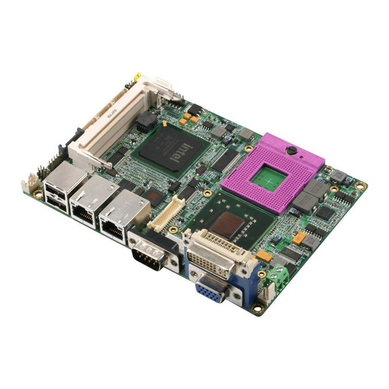
- Page 1 G E N E - 9 6 5 5 GENE-9655 ® ® Intel Core 2 Duo/Celeron M (65nm) Processors ® Intel 82574L for 10/100/1000Mbps Type II CompactFlash 4 COM, 6 USB2.0, Digital I/O Mini PCI/ Mini Card GENE-9655 Manual Rev.A 2nd Ed. June 2010...
-
Page 2: Copyright Notice
AAEON assumes no liabilities resulting from errors or omissions in this document, or from the use of the information contained herein. AAEON reserves the right to make changes in the product design without notice to its users. - Page 3 S u b C o m p a c t B o a r d G E N E - 9 6 5 5 Acknowledgments All other products’ name or trademarks are properties of their respective owners. Award is a trademark of Award Software International, Inc. CompactFlash™...
-
Page 4: Packing List
DVI-I to VGA Adapter • 9657666600 Jumper Cap • Cooler • Quick Installation Guide • CD-ROM for manual (in PDF format) and drivers • GENE-9655 If any of these items should be missing or damaged, please contact your distributor or sales representative immediately. -
Page 5: Table Of Contents
S u b C o m p a c t B o a r d G E N E - 9 6 5 5 Contents Chapter 1 General Information 1.1 Introduction..............1-2 1.2 Features ..............1-3 1.3 Specifications ............1-4 Chapter 2 Quick Installation Guide 2.1 Safety Precautions ............ - Page 6 S u b C o m p a c t B o a r d G E N E - 9 6 5 5 2.17 Digital I/O Connector (CN9) ........2-14 2.18 Fan Connector (CN10) ..........2-15 2.19 COM1 RS-232 Serial Port Connector (CN11) ..2-15 2.20 COM2 RS-232/422/485 Serial Port Connector (CN12) ..................
- Page 7 S u b C o m p a c t B o a r d G E N E - 9 6 5 5 Chapter 4 Driver Installation 4.1 Installation ..............4-3 Appendix A Programming The Watchdog Timer A.1 Programming ............A-2 A.2 ITE8781 Watchdog Timer Initial Program....A-6 Appendix B I/O Information B.1 I/O Address Map ............B-2...
-
Page 8: Chapter 1 General Information
S u b C o m p a c t B o a r d G E N E - 9 6 5 5 Chapter General Information 1- 1 Chapter 1 General Information... -
Page 9: Introduction
Moreover, one SATA II and one Type II CompactFlash storages are configured on the GENE-9655. In addition to the diverse storages, GENE-9655 also equips six USB2.0, four COM, one keyboard/mouse ports for flexible I/O expansions. There are no more worries about installing many necessary devices to complete the functions of your system. -
Page 10: Features
S u b C o m p a c t B o a r d G E N E - 9 6 5 5 1.2 Features ® ® Intel Core™ 2 Duo/ Celeron M (65nm) Processors Up To 2.2 GHz ®... -
Page 11: Specifications
S u b C o m p a c t B o a r d G E N E - 9 6 5 5 1.3 Specifications System Processor Socket 478M or onboard ® ® Intel Core™ 2 Duo/ Celeron (65nm) Processors up to 2.2GHz, FSB 533/667/800MHz System Memory 200-pin DDRII SODIMM x 1,... - Page 12 S u b C o m p a c t B o a r d G E N E - 9 6 5 5 ® Power Consumption Intel Core™ 2 Duo T7500 2.2 GHz, DDRII 667 2 GB, 4.12A @ +12V Board Size 5.75”(L) x 4”(W) (146mm x 101.6mm)
- Page 13 S u b C o m p a c t B o a r d G E N E - 9 6 5 5 Digital I/O Supports 8-bit (Programmable) Audio Line-in, Line-out, Mic-in, CD-in 1- 6 Chapter 1 General Information...
-
Page 14: Chapter 2 Quick Installation Guide
S u b C o m p a c t B o a r d G E N E - 9 6 5 5 Chapter Quick Installation Guide Notice: The Quick Installation Guide is derived from Chapter 2 of user manual. For other chapters further installation... -
Page 15: Safety Precautions
S u b C o m p a c t B o a r d G E N E - 9 6 5 5 2.1 Safety Precautions Always completely disconnect the power cord from your board whenever you are working on it. -
Page 16: Location Of Connectors And Jumpers
S u b C o m p a c t B o a r d G E N E - 9 6 5 5 2.2 Location of Connectors and Jumpers Component Side CN11 CN22 CN26 CN21 CN24 CN35 CN19 Chapter 2 Quick Installation Guide... -
Page 17: Solder Side
S u b C o m p a c t B o a r d G E N E - 9 6 5 5 Solder Side DIMM1 CN13 CFD1 Chapter 2 Quick Installation Guide... -
Page 18: Mechanical Drawing
S u b C o m p a c t B o a r d G E N E - 9 6 5 5 2.3 Mechanical Drawing Component Side 146.05 143.32 142.82 142.75 (10.04) (6.50) 132.84 132.84 121.18 93.43 84.24 (12.55) 80.26 73.92... - Page 19 S u b C o m p a c t B o a r d G E N E - 9 6 5 5 Solder Side 124.97 72.14 65.95 25.77 21.74 0.00 Chapter 2 Quick Installation Guide...
-
Page 20: List Of Jumpers
S u b C o m p a c t B o a r d G E N E - 9 6 5 5 2.4 List of Jumpers The board has a number of jumpers that allow you to configure your system to suit your application. -
Page 21: List Of Connectors
S u b C o m p a c t B o a r d G E N E - 9 6 5 5 2.5 List of Connectors The board has a number of connectors that allow you to configure your system to suit your application. - Page 22 S u b C o m p a c t B o a r d G E N E - 9 6 5 5 CN27 USB Connector CN28 USB Connector CN29 USB Connector CN30 USB Connector CN36 +5V Output Connector for 2.5” SATA Hard Disk CN37 UIM Connector for SIM BAT1...
-
Page 23: Setting Jumpers
S u b C o m p a c t B o a r d G E N E - 9 6 5 5 2.6 Setting Jumpers You configure your card to match the needs of your application by setting jumpers. A jumper is the simplest kind of electric switch. It consists of two metal pins and a small metal clip (often protected by a plastic cover) that slides over the pins to connect them. -
Page 24: Clear Cmos (Jp1)
S u b C o m p a c t B o a r d G E N E - 9 6 5 5 2.7 Clear CMOS (JP1) Function Protected (Default) Clear 2.8 LVDS LCD +5V/+3.3V Selection (JP2) Function +3.3V (Default) 2.9 LCD Backlight +5V/+12V Selection (JP3) Function +12V... -
Page 25: Lcd Backlight Voltage / Pwm Control Selection (Jp7)
S u b C o m p a c t B o a r d G E N E - 9 6 5 5 2.12 LCD Backlight Voltage / PWM Control Selection (JP7) Function Voltage Control (Default) PWM Control 2.13 VGA/ DVI Display Connector (CN2) Signal Signal DVI_TDC2#... -
Page 26: Lvds Lcd Connector (Cn4)
S u b C o m p a c t B o a r d G E N E - 9 6 5 5 GREEN BLUE HSYNC 2.14 LVDS LCD Connector (CN4) Note: For VLCD (pin 3, 7, 27), the max rating of each pin is 5V@0.5A Name Name L_BKLT_EN... -
Page 27: Audio Connector (Cn8)
S u b C o m p a c t B o a r d G E N E - 9 6 5 5 INV_EN 2.16 Audio Connector (CN8) Signal Signal MIC_L MIC_R GNDAUD CD_GND LIN_L CD_L LIN_R CD_GND GNDAUD CD_R LOUT_L LOUT_R... -
Page 28: Fan Connector (Cn10)
S u b C o m p a c t B o a r d G E N E - 9 6 5 5 Port 7 @2A4h Pin 7 GPIO Set 5 / Bit 1 U6 Pin 10 (GPIO 51) Port 6 @2A2h Pin 6 GPIO Set 3 / Bit 7... -
Page 29: Com2 Rs-232/422/485 Serial Port Connector (Cn12)
S u b C o m p a c t B o a r d G E N E - 9 6 5 5 2.20 COM2 RS-232/422/485 Serial Port Connector (CN12) RS-232 Mode Signal Signal DCDB DTRB Ground DSRB RTSB CTSB RIB / +5 Volt. -
Page 30: Ps/2 Keyboard/Mouse Connector (Cn19)
S u b C o m p a c t B o a r d G E N E - 9 6 5 5 RTSC CTSC DTRC 2.22 PS/2 Keyboard/Mouse Connector (CN19) Signal Signal KBDAT KBCLK KB_GND +5V_DUAL MSDAT MSCLK 2.23 COM4 RS-232 Serial Port Connector (CN20) Signal DCDD... -
Page 31: Standby Power Output W/Pson#/Smbus
S u b C o m p a c t B o a r d G E N E - 9 6 5 5 2.24 +5V Standby Power Output w/PSON#/SMBus Connector (CN24) Signal SMBDAT_SBY SMBCLK_SBY PS_ON# +5V_DUAL 2.25 Power Input Connector (CN25) Signal +12V_DUAL 2.26 Front Panel (CN26) -
Page 32: Usb Connector (Cn28)
S u b C o m p a c t B o a r d G E N E - 9 6 5 5 USBD2+ 2.28 USB Connector (CN28) Signal +5V_DUAL USBD3- USBD3+ 2.29 USB Connector (CN29) Signal +5V_DUAL USBD4- USBD4+ 2.30 USB Connector (CN30) Signal... -
Page 33: Output Connector For 2.5" Sata Hard Disk (Cn36)
S u b C o m p a c t B o a r d G E N E - 9 6 5 5 2.31 +5V Output Connector for 2.5” SATA Hard Disk (CN36) Note: The max. rating is 5V@1A Signal 2.32 UIM Connector for SIM (CN37) Signal... - Page 34 S u b C o m p a c t B o a r d G E N E - 9 6 5 5 +3.3V IRQ15 +3.3V +3.3V CSEL# SEC_IDERST# SIORDY SDA2 SDDREQ SDA1 DACK# SDA0 DASP# SDD0 PDIAG# SDD1 SDD8 SDD2 SDD9...
- Page 35 S u b C o m p a c t B o a r d G E N E - 9 6 5 5 Below Table for China RoHS Requirements 产品中有毒有害物质或元素名称及含量 AAEON Main Board/ Daughter Board/ Backplane 有毒有害物质或元素 部件名称 铅...
-
Page 36: Chapter 3 Award Bios Setup
S u b C o m p a c t B o a r d G E N E - 9 6 5 5 Chapter Award BIOS Setup Chapter 3 Award BIOS Setup 3-1... -
Page 37: System Test And Initialization
3. The CMOS memory has lost power and the configuration information has been erased. The GENE-9655 CMOS memory has an integral lithium battery backup for data retention. However, you will need to replace the complete unit when it finally runs down. -
Page 38: Award Bios Setup
S u b C o m p a c t B o a r d G E N E - 9 6 5 5 3.2 Award BIOS Setup Awards BIOS ROM has a built-in Setup program that allows users to modify the basic system configuration. This type of information is stored in battery-backed CMOS RAM so that it retains the Setup information when the power is turned off. - Page 39 Exit Without Saving Abandon all CMOS value changes and exit setup. You can refer to the “ AAEON BIOS Item Description.pdf” file in the CD for the meaning of each setting in this chapter. Chapter 3 Award BIOS Setup 3-4...
-
Page 40: Chapter 4 Driver Installation
S u b C o m p a c t B o a r d G E N E - 9 6 5 5 Chapter Driver Installation 4 -1 Chapter 4 Driver Installation... - Page 41 S u b C o m p a c t B o a r d G E N E - 9 6 5 5 The GENE-9655 comes with an AutoRun CD-ROM that contains all drivers and utilities that can help you to install the driver automatically.
- Page 42 S u b C o m p a c t B o a r d G E N E - 9 6 5 5 4.1 Installation: Insert the GENE-9655 CD-ROM into the CD-ROM drive. And install the drivers from Step 1 to Step 5 in order. Step 1 – Install INF Driver 1.
- Page 43 S u b C o m p a c t B o a r d G E N E - 9 6 5 5 Step 4 –Install Audio Driver 1. Click on the Step 4- ALC888 folder and select the OS folder your system is 2.
-
Page 44: Appendix A Programming The Watchdog Timer
S u b C o m p a c t B o a r d G E N E - 9 6 5 5 Appendix Programming the Watchdog Timer Appendix A Programming the Watchdog Timer A-1... -
Page 45: Programming
S u b C o m p a c t B o a r d G E N E - 9 6 5 5 A.1 Programming GENE-9655 utilizes ITE 8781 chipset as its watchdog timer controller. Below are the procedures to complete its configuration and the AAEON initial watchdog timer program is also attached based on which you can develop customized program to fit your application. - Page 46 S u b C o m p a c t B o a r d G E N E - 9 6 5 5 There are three steps to complete the configuration setup: (1) Enter the MB PnP Mode; (2) Modify the data of configuration registers; (3) Exit the MB PnP Mode.
- Page 47 S u b C o m p a c t B o a r d G E N E - 9 6 5 5 WatchDog Timer Configuration Registers Configure Control (Index=02h) This register is write only. Its values are not sticky; that is to say, a hardware reset will automatically clear the bits, and does not require the software to clear them.
- Page 48 S u b C o m p a c t B o a r d G E N E - 9 6 5 5 Watch Dog Timer 1, 2, 3 Configuration Register (Index=72h, 82h, 92h Default=001s0000b) Watch Dog Timer 1,2,3 Time-Out Value (LSB) Register (Index=73h,83h,93h, Default=38h) Watch Dog Timer 1,2,3 Time-Out Value (MSB) Register (Index=74h,84h,94h Default=00h)
-
Page 49: Ite8781 Watchdog Timer Initial Program
S u b C o m p a c t B o a r d G E N E - 9 6 5 5 A.2 ITE8781 Watchdog Timer Initial Program .MODEL SMALL .CODE Main: CALL Enter_Configuration_mode CALL Check_Chip mov cl, 7 call Set_Logic_Device ;time setting mov cl, 10 ;... - Page 50 S u b C o m p a c t B o a r d G E N E - 9 6 5 5 call Superio_Set_Reg ; game port enable mov cl, 9 call Set_Logic_Device Initial_OK: CALL Exit_Configuration_mode MOV AH,4Ch INT 21h Enter_Configuration_Mode PROC NEAR MOV SI,WORD PTR CS:[Offset Cfg_Port]...
- Page 51 S u b C o m p a c t B o a r d G E N E - 9 6 5 5 CALL Write_Configuration_Data Exit_Configuration_Mode ENDP Check_Chip PROC NEAR MOV AL,20h CALL Read_Configuration_Data CMP AL,87h JNE Not_Initial MOV AL,21h CALL Read_Configuration_Data CMP AL,81h JNE Not_Initial...
- Page 52 S u b C o m p a c t B o a r d G E N E - 9 6 5 5 OUT DX,AL MOV DX,WORD PTR CS:[Cfg_Port+06h] IN AL,DX Read_Configuration_Data ENDP Write_Configuration_Data PROC NEAR MOV DX,WORD PTR CS:[Cfg_Port+04h] OUT DX,AL XCHG AL,AH MOV DX,WORD PTR CS:[Cfg_Port+06h]...
- Page 53 S u b C o m p a c t B o a r d G E N E - 9 6 5 5 Set_Logic_Device proc near push ax push cx xchg al,cl mov cl,07h call Superio_Set_Reg pop cx pop ax Set_Logic_Device endp ;Select 02Eh->Index Port, 02Fh->Data Port Cfg_Port DB 087h,001h,055h,055h...
-
Page 54: Appendix B I/O Information
S u b C o m p a c t B o a r d G E N E - 9 6 5 5 Appendix I/O Information B - 1 Appendix B I/O Information... -
Page 55: I/O Address Map
S u b C o m p a c t B o a r d G E N E - 9 6 5 5 B.1 I/O Address Map B - 2 Appendix B I/O Information... -
Page 56: St Mb Memory Address Map
S u b C o m p a c t B o a r d G E N E - 9 6 5 5 B.2 1 MB Memory Address Map B - 3 Appendix B I/O Information... -
Page 57: Irq Mapping Chart
S u b C o m p a c t B o a r d G E N E - 9 6 5 5 B.3 IRQ Mapping Chart B.4 DMA Channel Assignments B - 4 Appendix B I/O Information... -
Page 58: Appendix C Mating Connector
S u b C o m p a c t B o a r d G E N E - 9 6 5 5 Appendix Mating Connecotor C - 1 Appendix C Mating Connector... -
Page 59: List Of Mating Connectors And Cables
S u b C o m p a c t B o a r d G E N E - 9 6 5 5 C.1 List of Mating Connectors and Cables The table notes mating connectors and available cables. Connector Mating Connector Available Cable P/N... - Page 60 S u b C o m p a c t B o a r d G E N E - 9 6 5 5 External External AUX External AUX Power CN24 Power and Catch 2418HJ-06 5VSB PS_ON# Cable PS_ON# +12V Vin Power CN25 1702002010...
Need help?
Do you have a question about the GENE-9655 and is the answer not in the manual?
Questions and answers