Table of Contents
Advertisement
Quick Links
Advertisement
Table of Contents

Related Manuals for Aaeon GENE-KBU6


Summary of Contents for Aaeon GENE-KBU6
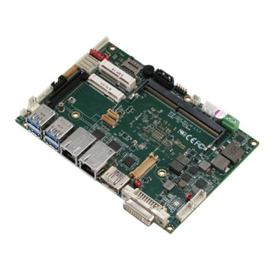
- Page 1 GENE-KBU6 3.5” Subcompact Board User’s Manual 1 Last Updated: June 30, 2017...
- Page 2 AAEON assumes no liabilities resulting from errors or omissions in this document, or from the use of the information contained herein. AAEON reserves the right to make changes in the product design without notice to its users.
- Page 3 Acknowledgement All other products’ name or trademarks are properties of their respective owners. Microsoft Windows is a registered trademark of Microsoft Corp. Intel, Pentium, Celeron, and Xeon are registered trademarks of Intel Corporation Core, Atom are trademarks of Intel Corporation ...
- Page 4 Before setting up your product, please make sure the following items have been shipped: Item Quantity GENE-KBU6 with heat spreader Product DVD with User’s Manual (in pdf) and drivers If any of these items are missing or damaged, please contact your distributor or sales representative immediately.
- Page 5 (if any), its specifications, dimensions, jumper/connector settings/definitions, and driver installation instructions (if any), to facilitate users in setting up their product. Users may refer to the AAEON.com for the latest version of this document. Preface...
- Page 6 Safety Precautions Please read the following safety instructions carefully. It is advised that you keep this manual for future references All cautions and warnings on the device should be noted. Make sure the power source matches the power rating of the device. Position the power cord so that people cannot step on it.
- Page 7 If any of the following situations arises, please the contact our service personnel: Damaged power cord or plug Liquid intrusion to the device iii. Exposure to moisture Device is not working as expected or in a manner as described in this manual The device is dropped or damaged Any obvious signs of damage displayed on the device...
- Page 8 FCC Statement This device complies with Part 15 FCC Rules. Operation is subject to the following two conditions: (1) this device may not cause harmful interference, and (2) this device must accept any interference received including interference that may cause undesired operation.
- Page 9 China RoHS Requirements (CN) 产品中有毒有害物质或元素名称及含量 AAEON Main Board/ Daughter Board/ Backplane 有毒有害物质或元素 部件名称 铅 汞 镉 六价铬 多溴联苯 多溴二苯醚 (Pb) (Hg) (Cd) (Cr(VI)) (PBB) (PBDE) 印刷电路板 ○ ○ ○ ○ ○ ○ 及其电子组件 外部信号 ○ ○ ○ ○ ○ ○...
- Page 10 China RoHS Requirement (EN) Poisonous or Hazardous Substances or Elements in Products AAEON Main Board/ Daughter Board/ Backplane Poisonous or Hazardous Substances or Elements Hexavalent Polybrominated Polybrominated Component Lead Mercury Cadmium Chromium Biphenyls Diphenyl Ethers (Pb) (Hg) (Cd) (Cr(VI)) (PBB) (PBDE) PCB &...
- Page 11 Table of Contents Chapter 1 - Product Specifications..................1 Specifications ......................2 Chapter 2 – Hardware Information ..................4 Dimensions ....................... 5 Jumpers and Connectors ..................8 Assembly Options ....................9 Block Diagram ......................11 List of Jumpers ......................12 2.5.1 Clear CMOS Jumper (JP1) ..............
- Page 12 2.6.7 LAN (RJ-45) Port1 (CN9) ..............22 2.6.8 LAN (RJ-45) Port2 (CN10) ..............23 2.6.9 Mini-Card Slot (Full-Mini Card) (CN11) ..........23 2.6.10 Micro SIM Card Socket (CN12) ............26 2.6.11 Mini-Card Slot (Half-Mini Card) (CN13) .......... 26 2.6.12 SATA Port 1 (CN14) ................28 2.6.13 +5V Output for SATA HDD (CN15) ..........
- Page 13 Setup submenu: Main ................... 51 Setup submenu: Advanced ................. 52 3.4.1 Advanced: CPU Configuration ............53 3.4.2 Trusted Computing ................55 SATA Configuration ....................57 Hardware Monitor ....................58 Smart Fan Mode Configuration ................59 SIO Configuration ....................63 Serial Port Configuration..................64 3.10 Serial Port Configuration..................
- Page 14 3.242 Setup Submenu: Exit ....................81 Chapter 4 – Drivers Installation .................... 83 Product CD/DVD ....................84 Note on EHCI ......................88 Appendix A - Watchdog Timer Programming ..............89 Watchdog Timer Registers .................. 90 Watchdog Sample Program ................. 91 Appendix B - I/O Information ....................
- Page 15 DI/O Programming ..................... 106 Digital I/O Register ....................107 Digital I/O Sample Program ................108 Appendix E – List of Mating Connectors and Cables ............111 Electrical Specifications for I/O Ports ..............112 Preface...
-
Page 16: Chapter 1 - Product Specifications
Chapter 1 Chapter 1 - Product Specifications... -
Page 17: Specifications
Specifications System 3.5'' SubCompact Board Form Factor Intel® Skylake-U i7-7600U/i5-7300U SoC Processor up to 3.4GHz CPU Frequency Intel® Skylake-U SoC Processor Chipset DDR4 1866/2133, SODIMM x1 Memory Type Up to 16 GB Max Memory Capacity ... - Page 18 Certification CE/FCC Display VGA/LCD Controller Intel® Skylake-U SoC Processor DVI, CRT/DP , LVDS Video Output (CRT is shared with DP , and default is DP) Backlight Inverter Supply Intel I210, 10/100/1000Base , RJ-45 x 2 (supports Ethernet ...
-
Page 19: Chapter 2 – Hardware Information
Chapter 2 Chapter 2 – Hardware Information... -
Page 20: Dimensions
Dimensions Component Side Component Side Chapter 2 – Hardware Information... -
Page 21: Solder Side
Solder Side (with heat spreader) Solder Side unit mm Chapter 2 – Hardware Information... - Page 22 Cooler Option (Part Number: 17592SKU60) Chapter 2 – Hardware Information...
-
Page 23: Jumpers And Connectors
Jumpers and Connectors Component Side Chapter 2 – Hardware Information... -
Page 24: Assembly Options
Assembly Options Option 1 Chapter 2 – Hardware Information... - Page 25 Option 2 Chapter 2 – Hardware Information...
-
Page 26: Block Diagram
Block Diagram Chapter 2 – Hardware Information... -
Page 27: List Of Jumpers
List of Jumpers Please refer to the table below for all of the board’s jumpers that you can configure for your application Label Function Clear CMOS Jumper LVDS Port Backlight Inverter VCC Selection LVDS Port Backlight Lightness Control Mode Selection LVDS Port Operating VDD Selection mSATA/Mini-Card Operating VCC Selection Touch Screen 4/5/8-wire Mode Selection... -
Page 28: Clear Cmos Jumper (Jp1)
2.5.1 Clear CMOS Jumper (JP1) Normal (Default) Clear CMOS 2.5.2 LVDS Port Backlight Inverter VCC Selection (JP2) +12V +5V (Default) 2.5.3 LVDS Port Backlight Lightness Control Mode Selection (JP3) 1 2 3 VR Mode (Default) PWM Mode 2.5.4 LVDS Port Operating VDD Selection (JP4) 1 2 3 +3.3V (Default) Chapter 2 –... -
Page 29: Msata/ Mini-Card Operating Vcc Selection (Jp5)
2.5.5 mSATA/ Mini-Card Operating VCC Selection (JP5) 1 2 3 mSATA (Default) Mini-Card 2.5.6 Touch Screen 4,5,8 Wire Selection (JP6) 1 2 3 4/8 WireS Mode (Default) 5 Wires Mode 2.5.7 Auto Power Button Enable/Disable Selection (JP7) 1 2 3 Disable Enable (Default) * When disabled, use power button JP10(1-2) to power on the system. -
Page 30: Com3 Pin8 Function Selection (Jp9)
2.5.9 COM3 Pin8 Function Selection (JP9) Ring (Default) +12V 2.5.10 Front Panel Connector (JP10) Pin Name Pin Name PWR_BTN- PWR_BTN+ HDD_LED- HDD_LED+ SPEAKER- SPEAKER+ PWR_LED- PWR_LED+ H/W RESET- H/W RESET+ 2.5.11 COM4 Pin8 Function Selection (JP11) Ring (Default) +12V Chapter 2 – Hardware Information... -
Page 31: List Of Connectors
List of Connectors Please refer to the table below for all of the board’s connectors that you can configure for your application. Label Function Battery DVI-I (Digital and Analog) DP Port LVDS Port LVDS Port Inverter / Backlight Connector SPI Debug Port LAN (RJ-45) Port1 CN10 LAN (RJ-45) Port2... - Page 32 CN28 COM Port 3 CN29 LPC Port CN30 External Power Input CN32 +5VSB Output w/SMBus CN33 External +5VSB Input CN35 BIO Connector CN36 CPU FAN Chapter 2 – Hardware Information...
-
Page 33: Battery (Cn1)
2.6.1 Battery (CN1) Pin Name Signal Type Signal level +3.3V 3.3V 2.6.2 DVI-I (Digital and Analog) (CN3) Pin Name Signal Type Signal Level DVI_D2- DVI_D2+ VGA_DDC_CLK VGA_DDC_DAT VGA_VSYNC DVI_D1- DVI_D1+ DVI_D0- DVI_D0+ Chapter 2 – Hardware Information... -
Page 34: Dp Port (Cn5)
DVI_CLK+ DVI_CLK- VGA_RED VGA_GREEN VGA_BLUE VGA_HSYNC 2.6.3 DP Port (CN5) Pin Name Signal Type Signal Level DP_D0+ DIFF DP_D0- DIFF DP_D1+ DIFF DP_D1- DIFF DP_D2+ DIFF DP_D2- DIFF DP_D3+ DIFF DP_D3- DIFF DP_AUX+ DIFF Chapter 2 – Hardware Information... -
Page 35: Lvds Port (Cn6)
DP_AUX- DIFF HPLG_DETECT 2.6.4 LVDS Port (CN6) *LVDS LCD_PWR can be set to +3.3V or +5V by JP4 Pin Name Signal Type Signal Level BKL_ENABLE BKL_CONTROL LCD_PWR +3.3V/+5V LVDS_A_CLK- DIFF LVDS_A_CLK+ DIFF LCD_PWR +3.3V/+5V LVDS_DA0- DIFF LVDS_DA0+ DIFF Chapter 2 – Hardware Information... -
Page 36: Lvds Port Inverter / Backlight Connector (Cn7)
LVDS_DA1- DIFF LVDS_DA1+ DIFF LVDS_DA2- DIFF LVDS_DA2+ DIFF LVDS_DA3- DIFF LVDS_DA3+ DIFF DDC_DATA +3.3V DDC_CLK +3.3V LVDS_DB0- DIFF LVDS_DB0+ DIFF LVDS_DB1- DIFF LVDS_DB1+ DIFF LVDS_DB2- DIFF LVDS_DB2+ DIFF LVDS_DB3- DIFF LVDS_DB3+ DIFF LCD_PWR +3.3V/+5V LVDS_B_CLK- DIFF LVDS_B_CLK+ DIFF 2.6.5 LVDS Port Inverter / Backlight Connector (CN7) BLK_PWR BKL_CONTROL BKL_ENABLE... -
Page 37: Spi Debug Port (Cn8)
Pin Name Signal Type Signal level BKL_PWR +5V / +12V BKL_CONTROL BKL_ENABLE * LVDS BKL_PWR can be set to +5V or +12V by JP2 * LVDS BKL_CONTROL can be set by JP3 2.6.6 SPI Debug Port (CN8) Pin Name Signal Type Signal Level SPI_MISO SPI_CLK... -
Page 38: Lan (Rj-45) Port2 (Cn10)
MDI0- DIFF MDI1+ DIFF MDI2+ DIFF MDI2- DIFF MDI1- DIFF MDI3+ DIFF MDI3- DIFF 2.6.8 LAN (RJ-45) Port2 (CN10) Pin Name Signal Type Signal level MDI0+ DIFF MDI0- DIFF MDI1+ DIFF MDI2+ DIFF MDI2- DIFF MDI1- DIFF MDI3+ DIFF MDI3- DIFF 2.6.9 Mini-Card Slot (Full-Mini Card) (CN11) Pin Name... - Page 39 +3.3VSB +3.3V +1.5V +1.5V PCIE_CLK_REQ# UIM_PWR UIM_DATA PCIE_REF_CLK- DIFF UIM_CLK PCIE_REF_CLK+ DIFF UIM_RST UIM_VPP W_DISABLE# +3.3V PCIE_RST# +3.3V PCIE_RX- DIFF +3.3VSB +3.3V PCIE_RX+ DIFF +1.5V +1.5V Chapter 2 – Hardware Information...
- Page 40 SMB_CLK +3.3V PCIE_TX- DIFF SMB_DATA +3.3V PCIE_TX+ DIFF USB_D- DIFF USB_D+ DIFF +3.3VSB +3.3V +3.3VSB +3.3V +1.5V +1.5V +3.3VSB +3.3V Chapter 2 – Hardware Information...
-
Page 41: Micro Sim Card Socket (Cn12)
2.6.10 Micro SIM Card Socket (CN12) Pin Name Signal Type Signal Level UIM_PWR UIM_RST UIM_CLK UIM_VPP UIM_DATA 2.6.11 Mini-Card Slot (Half-Mini Card) (CN13) Pin Name Signal Type Signal Level PCIE_WAKE# +3.3VSB +3.3V +1.5V +1.5V PCIE_CLK_REQ# PCIE_REF_CLK- DIFF Chapter 2 – Hardware Information... - Page 42 PCIE_REF_CLK+ DIFF W_DISABLE# +3.3V PCIE_RST# +3.3V PCIE_RX-/mSATA_RX+ DIFF +3.3VSB +3.3V PCIE_RX+/mSATA_RX- DIFF +1.5V +1.5V SMB_CLK +3.3V PCIE_TX-/mSATA_TX- DIFF SMB_DATA +3.3V PCIE_TX+/mSATA_TX+ DIFF USB_D- DIFF USB_D+ DIFF +3.3VSB +3.3V Chapter 2 – Hardware Information...
-
Page 43: Sata Port 1 (Cn14)
+3.3VSB +3.3V +1.5V +1.5V +3.3VSB +3.3V * CN13 can be selected for Mini-Card or mSATA by changing BIOS 2.6.12 SATA Port 1 (CN14) Pin 1 Pin 7 Pin Name Signal Type Signal Level SATA_TX+ DIFF SATA_TX- DIFF SATA_RX- DIFF SATA_RX+ DIFF Chapter 2 –... -
Page 44: V Output For Sata Hdd (Cn15)
2.6.13 +5V Output for SATA HDD (CN15) Pin Name Signal Type Signal Level 2.6.14 USB 3.0 Ports (CN18) Pin Name Signal Type Signal Level +5VSB USB_D- DIFF USB_D+ DIFF USB_SSRX− DIFF USB_SSRX+ DIFF USB_SSTX− DIFF USB_SSTX+ DIFF +5VSB USB_D- DIFF USB_D+ DIFF Chapter 2 –... -
Page 45: Usb 3.0 Ports (Cn19)
USB_SSRX− DIFF USB_SSRX+ DIFF USB_SSTX− DIFF USB_SSTX+ DIFF 2.6.15 USB 3.0 Ports (CN19) Pin Name Signal Type Signal Level +5VSB USB_D- DIFF USB_D+ DIFF USB_SSRX− DIFF USB_SSRX+ DIFF USB_SSTX− DIFF USB_SSTX+ DIFF +5VSB USB_D- DIFF USB_D+ DIFF Chapter 2 – Hardware Information... -
Page 46: Usb 2.0 Port (Cn20)
USB_SSRX− DIFF USB_SSRX+ DIFF USB_SSTX− DIFF USB_SSTX+ DIFF 2.6.16 USB 2.0 Port (CN20) +5VSB USB3_D- USB3_D+ Pin Name Signal Type Signal Level +5VSB USB_D- DIFF USB_D+ DIFF 2.6.17 USB 2.0 Port (CN21) +5VSB USB2_D- USB2_D+ Pin Name Signal Type Signal Level +5VSB Chapter 2 –... -
Page 47: Audio I/O Port (Cn22)
USB_D- DIFF USB_D+ DIFF G ND 2.6.18 Audio I/O Port (CN22) Pin Name Signal Type Signal Level MIC_L MIC_R GND_AUDIO LINE_L_IN LINE_R_IN GND_AUDIO LEFT_OUT GND_AUDIO RIGHT_OUT +5V_AUDIO Chapter 2 – Hardware Information... -
Page 48: Touchscreen Connector (Cn23)
2.6.19 Touchscreen Connector (CN23) * Touch mode can be set by JP6 4-Wire Pin Name Signal Type Signal Level BOTTOM LEFT RIGHT 4 Wires 5 Wires UL(Y) BOTTOM UR(H) LEFT LL(L) RIGHT LR(X) SENSE(S) 5-Wire Pin Name Signal Type Signal Level Chapter 2 –... - Page 49 UL(Y) UR(H) LL(L) LR(X) SENSE(S) 8-Wire Pin Name Signal Type Signal Level TOP EXCITE BOTTOM EXCITE LEFT EXCITE RIGHT EXCITE TOP SENSE BOTTOM SENSE LEFT SENSE RIGHT SENSE Chapter 2 – Hardware Information...
-
Page 50: Digital I/O Port (Cn24)
2.6.20 Digital I/O Port (CN24) Pin Name Signal Type Signal Level DIO0 DIO1 DIO2 DIO3 DIO4 DIO5 DIO6 DIO7 2.6.21 COM Port 1 (CN25) Pin Name Signal Type Signal Level Chapter 2 – Hardware Information... -
Page 51: Com Port 4 (Cn26)
±9V ±9V ±9V 2.6.22 COM Port 4 (CN26) RS-232 Pin Name Signal Type Signal Level ±5V ±5V ±5V RI/+5V/+12V IN/ PWR +5V/+12V Chapter 2 – Hardware Information... - Page 52 RS422_TX- RS422_TX+ RS422_RX+ RS422_RX- NC/+5V/+12V RS-422 Pin Name Signal Type Signal Level RS422_TX- ±5V RS422_TX+ ±5V RS422_RX+ RS422_RX- NC/+5V/+12V +5V/+12V RS-485 Pin Name Signal Type Signal Level RS485_D- ±5V Chapter 2 – Hardware Information...
-
Page 53: Com Port 2 (Cn27)
RS485_D+ ±5V NC/+5V/+12V +5V/+12V * COM4 RS-232/422/485 can be set by BIOS setting. Default is RS-232. * Pin 8 function can be set by JP11. 2.6.23 COM Port 2 (CN27) RS-232 Pin Name Signal Type Signal Level ±5V ±5V ±5V Chapter 2 –... - Page 54 RI/+5V/+12V IN/ PWR +5V/+12V RS-422 Pin Name Signal Type Signal Level RS422_TX- ±5V RS422_TX+ ±5V RS422_RX+ RS422_RX- NC/+5V/+12V +5V/+12V RS485_D- RS485_D+ NC/+5V/+12V RS-485 Chapter 2 – Hardware Information...
-
Page 55: Com Port 3 (Cn28)
Pin Name Signal Type Signal Level RS485_D- ±5V RS485_D+ ±5V NC/+5V/+12V +5V/+12V * COM2 RS-232/422/485 can be set by BIOS setting. Default is RS-232. * Pin 8 function can be set by JP9. 2.6.24 COM Port 3 (CN28) RS-232 Pin Name Signal Type Signal Level ±5V... - Page 56 ±5V ±5V RI/+5V/+12V IN/ PWR +5V/+12V RS-422 Pin Name Signal Type Signal Level RS422_TX- ±5V RS422_TX+ ±5V RS422_RX+ RS422_RX- NC/+5V/+12V +5V/+12V RS485_D- RS485_D+ NC/+5V/+12V Chapter 2 – Hardware Information...
-
Page 57: Lpc Port (Cn29)
RS-485 Pin Name Signal Type Signal Level RS485_D- ±5V RS485_D+ ±5V NC/+5V/+12V +5V/+12V * COM3 RS-232/422/485 can be set by BIOS setting. Default is RS-232. * Pin 8 function can be set by JP8. 2.6.25 LPC Port (CN29) Pin Name Signal Type Signal Level LAD0... -
Page 58: External Power Input (Cn30)
LFRAME# LRESET# +3.3V LCLK LDRQ0 LDRQ1 SERIRQ +3.3V 2.6.26 External Power Input (CN30) Pin Name Signal Type Signal Level +12V +9~+36V (or +12V) 2.6.27 +5VSB Output w/SMBus (CN32) Pin Name Signal Type Signal Level SMB_DATA +3.3V SMB_CLK +3.3V Chapter 2 – Hardware Information... -
Page 59: External +5Vsb Input (Cn33)
PS_ON# +3.3V +5VSB 2.6.28 External +5VSB Input (CN33) Pin Name Signal Type Signal Level PS_ON# +3.3V +5VSB 2.6.29 BIO Connector (CN35) Pin Name Signal Type Signal Level +12V_Dual +12V PCIE1_TX- PCIE1_RX- PCIE1_TX+ PCIE1_RX+ PCIE2_TX- Chapter 2 – Hardware Information... - Page 60 PCIE2_RX- PCIE2_TX+ PCIE2_RX+ PS_ON# +5V_Dual +5V_Dual +5V_Dual +5V_Dual PCIE_CLK+ PLT_RST# PCIE_CLK- Chapter 2 – Hardware Information...
- Page 61 USB 3.0_TX- USB 3.0_TX+ USB 2.0_D- USB 2.0_D+ USB 3.0_RX- USB 3.0_RX+ SMB_CLK SMB_DATA PCIE_WAKE# USB 2.0_OC# USB 2.0_OC# Chapter 2 – Hardware Information...
-
Page 62: Cpu Fan (Cn36)
LPC_AD0 LPC_FRAME# LPC_AD1 SERIRQ# LPC_AD2 LPC_AD3 GPIO Audio_GND LPC_CLK Audio_OUT_L PME# Audio_OUT_R 2.6.30 CPU Fan (CN36) Pin Name Signal Type Signal Level FAN_POWER +12V FAN_TAC Chapter 2 – Hardware Information... -
Page 63: Chapter 3 - Ami Bios Setup
Chapter 3 Chapter 3 - AMI BIOS Setup... -
Page 64: System Configuration Verification
System Test and Initialization These routines test and initialize board hardware. If the routines encounter an error during the tests, you will either hear a few short beeps or see an error message on the screen. There are two kinds of errors: fatal and non-fatal. The system can usually continue the boot up sequence with non-fatal errors. -
Page 65: Ami Bios Setup
AMI BIOS Setup AMI BIOS ROM has a built-in Setup program that allows users to modify the basic system configuration. This type of information is stored in battery-backed CMOS RAM and BIOS NVRAM so that it retains the Setup information when the power is turned off. Entering Setup Power on the computer and press <Del>or <ESC>... -
Page 66: Setup Submenu: Main
Setup submenu: Main Chapter 3 – AMI BIOS Setup... -
Page 67: Setup Submenu: Advanced
Setup submenu: Advanced Chapter 3 – AMI BIOS Setup... -
Page 68: Advanced: Cpu Configuration
3.4.1 Advanced: CPU Configuration Options summary: (default setting) Hyper-Threading Disabled Enabled Optimal Default, Failsafe Default Enabled for Windows XP and Linux (OS optimized for Hyper-Threading Technology) and Disabled for other OS (OS not optimized for Hyper-Threading Technology). Active Processor Optimal Default, Failsafe Default Cores Number of cores to enable in each processor package. - Page 69 Intel(R) SpeedStep(tm) Disabled Enabled Optimal Default, Failsafe Default Allows more than two frequency ranges to be supported. Turbo Mode Disabled Enabled Optimal Default, Failsafe Default Enable/Disable processor Turbo Mode (requires EMTTM enabled too). AUTO means enabled, unless max turbo ratio is bigger than 16 - SKL A0 W/A Chapter 3 –...
-
Page 70: Trusted Computing
3.4.2 Trusted Computing Options summary: (default setting) Security Device Disable Support Enable Optimal Default, Failsafe Default Enables or Disables BIOS support for security device. O.S. will not show Security Device. TCG EFI protocol and INT1A interface will not be available. SHA-1 PCR Bank Disable Enable... - Page 71 Platform Hierarchy Disable Enable Optimal Default, Failsafe Default Enable or Disable Platform Hierarchy Storage Hierarchy Disable Enable Optimal Default, Failsafe Default Enable or Disable Storage Hierarchy Endorsement Disable Hierarchy Enable Optimal Default, Failsafe Default Enable or Disable Endorsement Hierarchy TPM2.0 UEFI Spec TCG_2 Optimal Default, Failsafe Default Version...
-
Page 72: Sata Configuration
SATA Configuration Options summary: SATA Controller(s) Enabled Optimal Default, Failsafe Default Disabled Enable or disable SATA Device. SATA Mode AHCI Mode Optimal Default, Failsafe Default RAID Mode Determines how SATA controller(s) operate. Port 0 Disabled Enabled Optimal Default, Failsafe Default Enable or Disable SATA Port. -
Page 73: Hardware Monitor
Hardware Monitor Smart Fan Enabled Enable or Disable Smart Fan Disabled Chapter 3 – AMI BIOS Setup... -
Page 74: Smart Fan Mode Configuration
Smart Fan Mode Configuration Options summary: Fan Mode Manual Duty Auto Duty Optimal Default, Failsafe Default Smart Fan Mode Select Duty Cycle Auto fan speed control. Fan speed will follow different temperature by different Temoerature duty cycle 1-100 Chapter 3 – AMI BIOS Setup... - Page 75 Options summary: Manual Duty Mode 60 Optimal Default, Failsafe Default Manual mode fan control, user can write expected duty cycle (PWM fan type) 1-100 Chapter 3 – AMI BIOS Setup...
- Page 76 Options summary: Monitor Thermal CPU Temperature(DTS) Optimal Default, Failsafe Default Chassis Temperature(CPU) Chassis Temperature(PCH) Select monitor thermal source Temperature of Optimal Default, Failsafe Default Start Temperature Of Start Temperature Of Off 20 Optimal Default, Failsafe Default Temperature Of Off Start PWM Optimal Default, Failsafe Default Start PWM Chapter 3 –...
- Page 77 Slope (PWM) 0 (PWM) 1 (PWM) Optimal Default, Failsafe Default 2 (PWM) 4 (PWM) 8 (PWM) 16 (PWM) 32 (PWM) 64 (PWM) Slope (PWM) Chapter 3 – AMI BIOS Setup...
-
Page 78: Sio Configuration
SIO Configuration Chapter 3 – AMI BIOS Setup... -
Page 79: Serial Port Configuration
Serial Port Configuration Options summary: Use This Device Disabled Enabled Optimal Default, Failsafe Default En/Disable Serial Port (COM) Possible: Use Automatic Settings Optimal Default, Failsafe Default IO=3F8; IRQ=4; IO=2F8; IRQ=3; Select an optimal setting for IO device Chapter 3 – AMI BIOS Setup... -
Page 80: Serial Port Configuration
3.10 Serial Port Configuration Options summary: Use This Device Disabled Enabled Optimal Default, Failsafe Default En/Disable Serial Port (COM) Possible: Use Automatic Settings Optimal Default, Failsafe Default IO=2F8; IRQ=3; IO=3F8; IRQ=4; Mode: RS232 UART RS232, 422, 485 selection RS422 RS485 Select an optimal setting for IO device Chapter 3 –... -
Page 81: Serial Port Configuration
3.11 Serial Port Configuration Options summary: Use This Device Disabled Enabled Optimal Default, Failsafe Default En/Disable Serial Port (COM) Possible: Use Automatic Settings Optimal Default, Failsafe Default IO=3E8; IRQ=11; IO=2E8; IRQ=11; Mode: RS232 UART RS232, 422, 485 selection RS422 RS485 Select an optimal setting for IO device Chapter 3 –... -
Page 82: Serial Port Configuration
3.12 Serial Port Configuration Options summary: Use This Device Disabled Enabled Optimal Default, Failsafe Default En/Disable Serial Port (COM) Possible: Use Automatic Settings Optimal Default, Failsafe Default IO=2E8; IRQ=11; IO=3E8; IRQ=11; Mode: RS232 UART RS232, 422, 485 selection RS422 RS485 Select an optimal setting for IO device Chapter 3 –... -
Page 83: Usb Configuration
3.13 USB Configuration Options summary: Legacy USB Support Enabled Optimal Default, Failsafe Default Disabled Auto Enables BIOS Support for Legacy USB Support. When enabled, USB can be functional in legacy environment like DOS. AUTO option disables legacy support if no USB devices are connected Chapter 3 –... -
Page 84: Digital Io Port Configuration
3.14 Digital IO Port Configuration Options summary: DIO Port* Output Input Set DIO as Input or Output Output Level High Optimal Default, Failsafe Default Set output level when DIO pin is output Chapter 3 – AMI BIOS Setup... -
Page 85: Power Management
3.15 Power Management Options summary: Power Mode ATX Type Optimal Default, Failsafe Default AT Type Select system power mode. Power Saving(ERP) Disabled Optimal Default, Failsafe Default Control Enabled Configure power mode for power saving function. Restore on Power Last State Optimal Default, Failsafe Default Loss Power On... - Page 86 Resume from PCIE Disabled Enabled Optimal Default, Failsafe Default Enable/Disable Resume from PCIE Resume from Disabled LAN/RI Enabled Optimal Default, Failsafe Default Enable/Disable Resume from LAN/RI Chapter 3 – AMI BIOS Setup...
-
Page 87: Compatibility Support Module Configuration
3.16 Compatibility Support Module Configuration Boot option filter UEFI and Legacy Optimal Default, Failsafe Default Legacy only UEFI only This option controls Legacy/UEFI ROMs priority Storage Do not launch UEFI Legacy Optimal Default, Failsafe Default Controls the execution of UEFI and Legacy Storage OpROM Video Do not launch UEFI... -
Page 88: Setup Submenu: Chipset
3.17 Setup submenu: Chipset Chapter 3 – AMI BIOS Setup... -
Page 89: System Agent (Sa) Configuration
3.18 System Agent (SA) Configuration Options summary: Max TOLUD Dynamic Optimal Default, Failsafe Default 1 GB 1.25 GB 1.5 GB 1.75 GB 2 GB 2.25 GB 2.5 GB 2.75 GB 3 GB 3.25 GB 3.5 GB Maximum Value of TOLUD Dynamic assignment would adjust TOLUD automatically based on largest MMIO length of installed graphic controller. -
Page 90: Graphics Configuration
3.19 Graphics Configuration Options summary: Primary IGFX Boot VBIOS Default Optimal Default, Failsafe Default Display CRT/DP LVDS Select the Video Device which will be activated during POST. This has no effect if external graphic present. Secondary boot display selection will appear based on your selection. Secondary IGFX Boot Disabled Optimal Default, Failsafe Default... -
Page 91: Lvds Panel Configuration
3.20 LVDS Panel Configuration LVDS Disabled Enabled Optimal Default, Failsafe Default Enable/Disabled this panel. LVDS Panel Type 640x480,18bit,60Hz 800x480,18bit,60Hz 800x600,18bit,60Hz 1024x600,18bit,60Hz 1024x768,18bit,60Hz Optimal Default, Failsafe Default 1024x768,24bit,60Hz 1280x768,24bit,60Hz 1280x1024,48bit,60Hz 1366x768,24bit,60Hz 1440x900,48bit,60Hz 1600x1200,48bit,60Hz 1920x1080,48bit,60Hz 1920x1200,48bit,60Hz Select LCD panel used by Internal Graphics Device by selecting the appropriate setup item. - Page 92 Color Depth 18-bit Optimal Default, Failsafe Default 24-bit 36-bit 48-bit Select panel type Backlight Type Normal Optimal Default, Failsafe Default Inverted Select backlight control signal type Backlight Level Optimal Default, Failsafe Default 100% Select backlight control level Backlight PWM Freq 100Hz 200Hz 220Hz...
-
Page 93: Pch-Io Configuration
3.21 PCH-IO Configuration Options summary: HD Audio Disabled Enabled Optimal Default, Failsafe Default Control Detection of the HD-Audio device. Disabled = HDA will be unconditionally disabled Enabled = HDA will be unconditionally enabled Auto = HDA will be enabled if present, disabled otherwise. PCI Express Root Enabled Optimal Default, Failsafe Default... -
Page 94: Security
3.22 Security Change User/Supervisor Password You can install a Supervisor password, and if you install a supervisor password, you can then install a user password. A user password does not provide access to many of the features in the Setup utility. If you highlight these items and press Enter, a dialog box appears which lets you enter a password. - Page 95 3.23 Setup Submenu: Boot Options summary: Quiet Boot Disabled Enabled Optimal Default, Failsafe Default En/Disable showing boot logo. Launch PXE OpROM Disabled Optimal Default, Failsafe Default Enabled Controls the execution of UEFI and Legacy PXE OpROm Chapter 3 – AMI BIOS Setup...
-
Page 96: Bbs Priorities
BBS Priorities Chapter 3 – AMI BIOS Setup... -
Page 97: Setup Submenu: Exit
3.242 Setup Submenu: Exit Chapter 3 – AMI BIOS Setup... -
Page 98: Chapter 4 – Drivers Installation
Chapter 4 Chapter 4 – Drivers Installation... -
Page 99: Product Cd/Dvd
Product CD/DVD The GENE-SKU6 comes with a product DVD that contains all the drivers and utilities you need to setup your product. Insert the DVD and follow the steps in the autorun program to install the drivers. In case the program does not start, follow the sequence below to install the drivers. Step 1 –... - Page 100 Follow the instructions Drivers will be installed automatically Step 5 – Install USB 3.0 Driver (Windows 7 only) Open the Step5 - USB3.0 folder followed by Setup.exe Follow the instructions Drivers will be installed automatically Step 6 – Install TPM 2.0 Driver (Windows 7 only) Open the Step6 TPM 2.0 folder followed by the .msu file Follow the instructions Drivers will be installed automatically...
- Page 101 Step 8 – Install Serial Port Drivers For Windows 7: Change User Account Control settings to Never notify Reboot and log in as administrator Chapter 4 – Driver Installation...
- Page 102 Run patch.bat as administrator For Windows 8/10: Click on the Step8 - Serial Port Driver (Optional) folder and select your OS Open the setup.exe file in the folder Follow the instructions Drivers will be installed automatically Chapter 4 – Driver Installation...
-
Page 103: Note On Ehci
Note on EHCI With the EHCI controller no longer available on the 6th Gen Intel Core™ ® platforms, it is recommended to install Windows 7 through a SATA bus, eg SATA DVD-ROM, or patch the xHCI driver onto an installation media for Windows 7. -
Page 104: Appendix A - Watchdog Timer Programming
Appendix A Appendix A - Watchdog Timer Programming... -
Page 105: A.1 Watchdog Timer Registers
Watchdog Timer Registers Table 1 : Watch dog relative IO address Default Value Note I/O Base I/O Base address for Watchdog operation. 0xA10 Address This address is assigned by SIO LDN7, register 0x60-0x61. Table 2 : Watchdog relative register table Register Offset BitNum... -
Page 106: A.2 Watchdog Sample Program
A.2 Watchdog Sample Program ****************************************************************************** // WDT I/O operation relative definition (Please reference to Table 1) #define WDTAddr 0x510 // WDT I/O base address Void WDTWriteByte(byte Register, byte Value); byte WDTReadByte(byte Register); Void WDTSetReg(byte Register, byte Bit, byte Val); // Watch Dog relative definition (Please reference to Table 2) #define DevReg 0x00 // Device configuration register #define WDTRstBit 0x80 // Watchdog WDTRST# (Bit7) - Page 107 VOID AaeonWDTEnable (){ WDTEnableDisable(1); // Procedure : AaeonWDTConfig VOID AaeonWDTConfig (byte Counter, BOOLEAN Unit){ // Disable WDT counting WDTEnableDisable(0); // Clear Watchdog Timeout Status WDTClearTimeoutStatus(); // WDT relative parameter setting WDTParameterSetting(Timer, Unit); VOID WDTEnableDisable(byte Value){ If (Value == 1) WDTSetBit(TimerReg, EnableBit, 1); else WDTSetBit(TimerReg, EnableBit, 0);...
- Page 108 VOID WDTWriteByte(byte Register, byte Value){ IOWriteByte(WDTAddr+Register, Value); byte WDTReadByte(byte Register){ return IOReadByte(WDTAddr+Register); VOID WDTSetBit(byte Register, byte Bit, byte Val){ byte TmpValue; TmpValue = WDTReadByte(Register); TmpValue &= ~(1 << Bit); TmpValue |= Val << Bit; WDTWriteByte(Register, TmpValue); ******************************************************************************* Appendix A – Watchdog Timer Programming...
-
Page 109: Appendix B - I/O Information
Appendix B Appendix B - I/O Information... -
Page 110: B.1 I/O Address Map
I/O Address Map Appendix B – I/O Information... - Page 111 Appendix B – I/O Information...
-
Page 112: B.2 Memory Address Map
Memory Address Map Appendix B – I/O Information... - Page 113 Appendix B – I/O Information...
-
Page 114: B.3 Irq Mapping Chart
IRQ Mapping Chart Appendix B – I/O Information... - Page 115 Appendix B – I/O Information...
-
Page 116: Appendix C – Electrical Specifications For I/O Ports
Appendix C Appendix C – Electrical Specifications for I/O Ports... -
Page 117: C.1 Electrical Specifications For I/O Ports
Electrical Specifications for I/O Ports Reference Signal Name Rate Output DVI Port +5V/1A (reserved) DP port +3.3V +3.3V/1A +3.3V/2A or LVDS Port +3.3V/+5V +5V/2A LVDS Port Inverter / +5V/1.5A or +5V/+12V Backlight Connector +12V/1.5A Mini-Card Slot +3.3VSB +3.3V/1.1A CN11 (Full-Mini Card) +1.5V +1.5V/0.375A Mini-Card Slot... - Page 118 Audio I/O Port CN22 +5V/1A Digital IO Port CN24 +5V/1A +5V/0.5A or COM Port 4 CN26 +5V/+12V +12V/0.5A +5V/0.5A or COM Port 2 CN27 +5V/+12V +12V/0.5A +5V/0.5A or COM Port 3 CN28 +5V/+12V +12V/0.5A LPC Port CN29 +3.3V +3.3V/0.5A CPU FAN CN36 +12V +12V/0.5A...
-
Page 119: Appendix D – Digital I/O Ports
Appendix D Appendix D – Digital I/O Ports... -
Page 120: D.1 Electrical Specifications For Digital I/O Ports
Electrical Specifications for Digital I/O Ports Table 1 : Digital Input/Output Pin Electrical Specification Input Threshold Output Voltage Voltage Type Note High High DIO0 DIO1 DIO2 DIO3 DIO4 DIO5 DIO6 DIO7 Note: All DIO pins are 5V tolerant in input mode. Appendix D –... -
Page 121: D.2 Di/O Programming
DI/O Programming GENE-SKU6 utilizes FINTEK F81866D chipset as its Digital I/O controller. Below are the procedures to complete its configuration and the AAEON initial DI/O program is also attached, based on which you can develop customized program to fit your application. -
Page 122: D.3 Digital I/O Register
Digital I/O Register Table 2 : SuperIO relative register table Default Value Note SIO MB PnP Mode Index Register Index 0x2E 0x2E or 0x4E SIO MB PnP Mode Data Register Data 0x2F) 0x2F or 0x4F Table 3 : Digital Input/Output relative register table Register Note DIO0 Direction... -
Page 123: D.4 Digital I/O Sample Program
Digital I/O Sample Program ************************************************************************** // SuperIO relative definition (Please reference to Table 2) #define SIOIndex 0x2E #define SIOData 0x2F #define DIOLDN 0x06 IOWriteByte(byte IOPort, byte Value); IOReadByte(byte IOPort); // DIO relative definition (Please reference to Table 3) #define DirReg 0xA0 // 0:input, 1: output #define InputPin... - Page 124 // Input : Example, Set Digital I/O Pin 2 to high level AaeonSetOutputLevel(Pin2Bit, PinHigh); ************************************************************************** ************************************************************************** Boolean AaeonReadPinStatus(byte PinBit){ Boolean PinStatus ; PinStatus = SIOBitRead(DIOLDN, StatusReg, PinBit); Return PinStatus ; VOID AaeonSetOutputLevel(byte PinBit, byte Value){ ConfigDioMode(PinBit, OutputPin); SIOBitSet(DIOLDN, OutputReg, PinBit, Value); ******************************************************************************** ********************************************************************************VOID SIOEnterMBPnPMode(){...
- Page 125 IOWriteByte(SIOData, TmpValue); SIOExitMBPnPMode(); VOID SIOByteSet(byte LDN, byte Register, byte Value){ SIOEnterMBPnPMode(); SIOSelectLDN(LDN); IOWriteByte(SIOIndex, Register); IOWriteByte(SIOData, Value); SIOExitMBPnPMode(); ******************************************************************************** ******************************************************************************** Boolean SIOBitRead(byte LDN, byte Register, byte BitNum){ Byte TmpValue; SIOEnterMBPnPMode(); SIOSelectLDN(LDN); IOWriteByte(SIOIndex, Register); TmpValue = IOReadByte(SIOData); TmpValue &= (1 << BitNum); SIOExitMBPnPMode();...
-
Page 126: Appendix E – List Of Mating Connectors And Cables
Appendix E Appendix E – List of Mating Connectors and Cables... -
Page 127: E.1 Electrical Specifications For I/O Ports
Electrical Specifications for I/O Ports Mating Connector Connector Available Function Cable P/N Label Vendor Model no. Cable External Battery Molex 51021-0200 175011901C Cable Connector LVDS HIROSE DF13-30DS-1.25C Connector LVDS Inverter PHR-5 Connector SATA SATA CN14 Molex 88750-5318 1709070500 Connector Cable 2 Pins +5Vout CN15... - Page 128 Digital I/O CN24 Neltron 2026B-10 Connector COM Port Serial CN25 Molex 51021-0900 Port 1701090150 Connector Cable COM Port Serial CN26 Molex 51021-0900 Port 1701090150 Connector Cable COM Port Serial CN27 Molex 51021-0900 Port 1701090150 Connector Cable COM Port Serial CN28 Molex 51021-0900 Port...
- Page 129 CPU Fan CN36 Molex 22-01-2035 Connector Appendix E – Mating Connectors and Cables...
Need help?
Do you have a question about the GENE-KBU6 and is the answer not in the manual?
Questions and answers