
Subscribe to Our Youtube Channel
Related Manuals for Aaeon GENE-9310


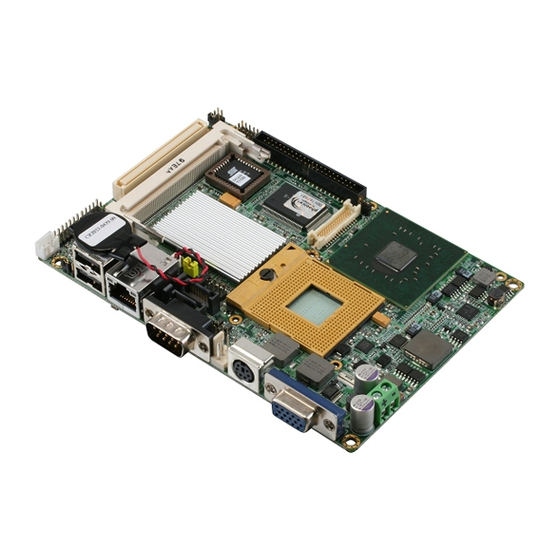
Summary of Contents for Aaeon GENE-9310
- Page 1 G E N E - 9 3 1 0 GENE-9310 ® Intel Core 2 Duo/ Core Duo/ ® Core Solo/ Celeron M (Yonah) Processors With LVDS, Ethernet, 2 Channel Audio & Mini PCI GENE-9310 Rev. A Manual 1st Ed. Jan. 2007...
-
Page 2: Copyright Notice
AAEON assumes no liabilities resulting from errors or omissions in this document, or from the use of the information contained herein. AAEON reserves the right to make changes in the product design without notice to its users. - Page 3 S u b C o m p a c t B o a r d G E N E - 9 3 1 0 Acknowledgments All other products’ name or trademarks are properties of their respective owners. Award is a trademark of Award Software International, Inc. CompactFlash™...
-
Page 4: Packing List
Quick Installation Guide • CD-ROM for manual (in PDF format) and drivers • 9681931000 Cable Kit for GENE-9310 • 9657666600 Jumper Cap If any of these items should be missing or damaged, please contact your distributor or sales representative immediately. -
Page 5: Table Of Contents
S u b C o m p a c t B o a r d G E N E - 9 3 1 0 Contents Chapter 1 General Information 1.1 Introduction..............1-2 1.2 Features ..............1-4 1.3 Specifications ............1-5 Chapter 2 Quick Installation Guide 2.1 Safety Precautions ............ - Page 6 S u b C o m p a c t B o a r d G E N E - 9 3 1 0 2.18 Fan Connector (CN15) ..........2-16 2.19 DC 12V Power Connector (CN19) ......2-16 2.20 USB Connector (CN20)........... 2-16 2.21 PS2 Keyboard/ Mouse Connector (CN21)....
- Page 7 S u b C o m p a c t B o a r d G E N E - 9 3 1 0 B.4 DMA Channel Assignments........B-4 Appendix C Mating Connector C.1 List of Mating Connectors and Cables....C-2...
-
Page 8: Chapter 1 General Information
S u b C o m p a c t B o a r d G E N E - 9 3 1 0 Chapter General Information 1- 1 Chapter 1 General Information... -
Page 9: Introduction
Furthermore, through expansion interface, customers can get four additional COM ports. Concerning the USB ports, GENE-9310 features a total of five USB 2.0 ports. Two are standard ports, and two are internal pin headers with the last one is extended from the extension card. - Page 10 In addition to making use of Intel’s revolutionary platform, GENE-9310 also offers flexibility of expansion requirements in terms of the above characteristics. Chapter 1 General Information...
-
Page 11: Features
S u b C o m p a c t B o a r d G E N E - 9 3 1 0 1.2 Features ® ® Intel Core 2 Duo/ Core Duo/ Core Solo/ Celeron (Yonah) Processors Supports 36-bit Dual Channel LVDS TFT Panel Supports TV-Out Supports DDRII 400/533/667 SODIMM Memory up to 2 CH AC97 2.3 Audio Codec... -
Page 12: Specifications
S u b C o m p a c t B o a r d G E N E - 9 3 1 0 1.3 Specifications System • CPU: ® Intel Core 2 Duo/ Core Duo/ ® Core Solo/ Celeron M (Yonah) Processors, FSB 533/667MHz Memory:... - Page 13 S u b C o m p a c t B o a r d G E N E - 9 3 1 0 101.6mm) Gross Weight: 0.88lb (0.4kg) Operating Temperature: 32°F~140°F (0°C~60°C) Storage Temperature: -40°F~176°F (-40°C~80°C) Operating Humidity: 0%~90% relative humidity, non-condensing Display: Supports CRT/LCD, CRT/TV, LCD/TV, simultaneous/dual view displays...
- Page 14 S u b C o m p a c t B o a r d G E N E - 9 3 1 0 RS-232/422/485 x 1 Audio: MIC-in, Line-in, Line-out, CD-in & S/P DIF in/out USB: 4 USB 2.0 Ports, Tow onboard and one 5x2 box header supports two USB ports Digital I/O:...
-
Page 15: Chapter 2 Quick Installation Guide
S u b C o m p a c t B o a r d G E N E - 9 3 1 0 Chapter Quick Installation Guide Notice: The Quick Installation Guide is derived from Chapter 2 of user manual. For other chapters further installation... -
Page 16: Safety Precautions
S u b C o m p a c t B o a r d G E N E - 9 3 1 0 2.1 Safety Precautions Always completely disconnect the power cord from your board whenever you are working on it. -
Page 17: Location Of Connectors And Jumpers
S u b C o m p a c t B o a r d G E N E - 9 3 1 0 2.2 Location of Connectors and Jumpers Component Side CN26 CN21 CN15 CN20 CN11 CN12 SATA1 CN22 SATA2 BAT1 LAN1... - Page 18 S u b C o m p a c t B o a r d G E N E - 9 3 1 0 Solder Side Chapter 2 Quick Installation Guide...
-
Page 19: Mechanical Drawing
S u b C o m p a c t B o a r d G E N E - 9 3 1 0 2.3 Mechanical Drawing Component Side 137.16 133.93 133.93 129.91 128.02 114.94 114.17 108.71 90.17 77.72 72.14 69.09 68.20 68.33... - Page 20 S u b C o m p a c t B o a r d G E N E - 9 3 1 0 (39.60) (14.20) (8.40) (7.90) DC FAN (1.60) (12.90) HEATSINK (12.55) (13.35) (17.30) Chapter 2 Quick Installation Guide...
- Page 21 S u b C o m p a c t B o a r d G E N E - 9 3 1 0 Solder Side Chapter 2 Quick Installation Guide...
-
Page 22: List Of Jumpers
S u b C o m p a c t B o a r d G E N E - 9 3 1 0 2.4 List of Jumpers The board has a number of jumpers that allow you to configure your system to suit your application. -
Page 23: List Of Connectors
S u b C o m p a c t B o a r d G E N E - 9 3 1 0 2.5 List of Connectors The board has a number of connectors that allow you to configure your system to suit your application. - Page 24 S u b C o m p a c t B o a r d G E N E - 9 3 1 0 USB1 USB Connector BAT1 RTC BATTERY Connector MPCI1 Mini PCI Slot SATA1 Primary Serial ATA Connector SATA2 Secondary Serial ATA Connector DIMM1...
-
Page 25: Setting Jumpers
S u b C o m p a c t B o a r d G E N E - 9 3 1 0 2.6 Setting Jumpers You configure your card to match the needs of your application by setting jumpers. A jumper is the simplest kind of electric switch. It consists of two metal pins and a small metal clip (often protected by a plastic cover) that slides over the pins to connect them. -
Page 26: Lvds(1)-Lcd(Cn12) Voltage Selection (Jp1)
S u b C o m p a c t B o a r d G E N E - 9 3 1 0 2.7 LVDS(1)-LCD(CN12) Voltage Selection (JP1) Function +3.3V (Default) 2.8 COM2 Ring/+5V/+12V Selection (JP3) Function +12V Ring (Default) 2.9 Clear CMOS (JP6) Function Protected (Default) -
Page 27: Digital I/O Connector (Cn2)
S u b C o m p a c t B o a r d G E N E - 9 3 1 0 2.12 Digital I/O Connector (CN2) This connector offers 4-pair of digital I/O functions and address is 801H. -
Page 28: Tv_Out Connector (Cn3)
S u b C o m p a c t B o a r d G E N E - 9 3 1 0 2.13 TV_Out Connector (CN3) Name Name CVBS N.C. N.C. 2.14 AC97 Audio Connector (CN6) Signal Signal First MIC IN Secondary MIC IN LINE_IN_GND... -
Page 29: Com1 Rs-232 Serial Port Connector (Cn11)
S u b C o m p a c t B o a r d G E N E - 9 3 1 0 2.16 COM1 RS-232 Serial Port Connector (CN11) Signal Signal 10.11 2.17 LVDS (1)-LCD Connector (CN12) Signal Signal BKLTEN BKLTCTL... -
Page 30: Fan Connector (Cn15)
S u b C o m p a c t B o a r d G E N E - 9 3 1 0 2.18 Fan Connector (CN15) Signal Speed Control +12V or +5V (Default) Speed Sense 2.19 DC12V Power Connector (CN19) Signal Signal +12V... -
Page 31: Eide Connector (Cn22)
S u b C o m p a c t B o a r d G E N E - 9 3 1 0 2.22 EIDE Connector (CN22) Signal Signal IDE RESET DATA7 DATA8 DATA6 DATA9 DATA5 DATA10 DATA4 DATA11 DATA3 DATA12 DATA2... -
Page 32: Front Panel Connector (Cn23)
S u b C o m p a c t B o a r d G E N E - 9 3 1 0 2.23 Front Panel Connector (CN23) Signal Signal Power On Button (-) Power On Button (+) IDE LED (-) IDE LED (+) External Buzzer (-) External Buzzer (+) -
Page 33: Expansion Board 140-Pin Slot (Cn25)
S u b C o m p a c t B o a r d G E N E - 9 3 1 0 IO WRITE +5V/+3.3V IRQ14 +5V/+3.3V N.C. CFDRST IO READY DACK UDMA DETECT DATA8 DATA9 DATA10 2.25 Expansion Board 140-pin Slot (CN25) Signal Signal +2.5V... - Page 34 S u b C o m p a c t B o a r d G E N E - 9 3 1 0 PCI_REQ#1 SDVO_FLDSTALL PCI_AD22 PCI_PAR INT_PIRQD# PCI_SLOT2_CLK33 PCI_SLOT1_CLK33 PCI_AD16 SMBCLK_SBY PCI_REQ#2 SMBDAT_SBY PCI_AD26 PCI_AD30 PCIE_WAKE# PCI_AD31 PCIE_RST# PCI_AD29 PCI_STOP# PCIE_TXP...
- Page 35 S u b C o m p a c t B o a r d G E N E - 9 3 1 0 PCI_AD4 +3.3V_DUAL PCI_AD9 +3.3V_DUAL PCI_AD15 PM_CLKRUN# PM_SLP_S3# PCI_SERR# PM_SLP_S4# PCI_AD6 PM_SLP_S5# PCI_PERR# INT_BAT# PCI_C/BE#1 +5V_DUAL PCI_AD0 +5V_DUAL PCI_AD2 +5V_DUAL...
-
Page 36: Vga Display Connector (Cn26)
S u b C o m p a c t B o a r d G E N E - 9 3 1 0 2.26 VGA Display Connector (CN26) Signal Signal GREEN BLUE N.C. CRT_PLUG N.C. DDCDAT HSYNC VSYNC DDCCLK H1, H2 N.C. -
Page 37: Chapter 3 Award Bios Setup
S u b C o m p a c t B o a r d G E N E - 9 3 1 0 Chapter Award BIOS Setup Chapter 3 Award BIOS Setup... -
Page 38: System Test And Initialization
3. The CMOS memory has lost power and the configuration information has been erased. The GENE-9310 CMOS memory has an integral lithium battery backup for data retention. However, you will need to replace the complete unit when it finally runs down. -
Page 39: Award Bios Setup
S u b C o m p a c t B o a r d G E N E - 9 3 1 0 3.2 Award BIOS Setup Awards BIOS ROM has a built-in Setup program that allows users to modify the basic system configuration. This type of information is stored in battery-backed CMOS RAM so that it retains the Setup information when the power is turned off. - Page 40 S u b C o m p a c t B o a r d G E N E - 9 3 1 0 Integrated Peripherals Use this menu to specify your settings for integrated peripherals. (Primary slave, secondary slave, keyboard, mouse etc.) Power Management Setup Use this menu to specify your settings for power...
-
Page 41: Save And Exit Setup
Save CMOS value changes to CMOS and exit setup. Exit Without Saving Abandon all CMOS value changes and exit setup. You can refer to the "AAEON BIOS Item Description.pdf" file in the CD for the meaning of each setting in this chapter. -
Page 42: Chapter 4 Driver Installation
S u b C o m p a c t B o a r d G E N E - 9 3 1 0 Chapter Driver Installation Chapter 4 Driver Installation... - Page 43 S u b C o m p a c t B o a r d G E N E - 9 3 1 0 The GENE-9310 comes with a CD-ROM that contains all drivers and utilities that meet your needs.
- Page 44 S u b C o m p a c t B o a r d G E N E - 9 3 1 0 4.1 Installation: Insert the GENE-9310 CD-ROM into the CD-ROM Drive. And install the drivers from Step 1 to Step 5 in order. Step 1 – Install Intel INF Driver 1.
- Page 45 S u b C o m p a c t B o a r d G E N E - 9 3 1 0 2. Double click on the WDM_A394.exe 3. Follow the instructions that the window shows 4. The system will help you install the driver automatically Step 5 –...
-
Page 46: Appendix A Programming The Watchdog Timer
S u b C o m p a c t B o a r d G E N E - 9 3 1 0 Appendix Programming the Watchdog Timer Appendix A Programming the Watchdog Timer... -
Page 47: Programming
S u b C o m p a c t B o a r d G E N E - 9 3 1 0 A.1 Programming GENE-9310 utilizes ITE 8712 chipset as its watchdog timer controller. Below are the procedures to complete its configuration and the... - Page 48 S u b C o m p a c t B o a r d G E N E - 9 3 1 0 registers; (3) Exit the MB PnP Mode. Undesired result may occur if the MB PnP Mode is not exited normally. (1) Enter the MB PnP Mode To enter the MB PnP Mode, four special I/O write operations are to be performed during Wait for Key state.
- Page 49 S u b C o m p a c t B o a r d G E N E - 9 3 1 0 WatchDog Timer Configuration Registers Configure Control (Index=02h) This register is write only. Its values are not sticky; that is to say, a hardware reset will automatically clear the bits, and does not require the software to clear them.
- Page 50 S u b C o m p a c t B o a r d G E N E - 9 3 1 0 WatchDog Timer Control Register (Index=71h, Default=00h) WatchDog Timer Configuration Register (Index=72h, Default=00h) WatchDog Timer Time-out Value Register (Index=73h, Default=00h) Appendix A Programming the Watchdog Timer...
-
Page 51: It8712 Watchdog Timer Initial Program
S u b C o m p a c t B o a r d G E N E - 9 3 1 0 A.2 IT8712 Watchdog Timer Initial Program .MODEL SMALL .CODE Main: CALL Enter_Configuration_mode CALL Check_Chip mov cl, 7 call Set_Logic_Device ;time setting mov cl, 10 ;... - Page 52 S u b C o m p a c t B o a r d G E N E - 9 3 1 0 ; game port enable mov cl, 9 call Set_Logic_Device Initial_OK: CALL Exit_Configuration_mode MOV AH,4Ch INT 21h Enter_Configuration_Mode PROC NEAR MOV SI,WORD PTR CS:[Offset Cfg_Port] MOV DX,02Eh...
- Page 53 S u b C o m p a c t B o a r d G E N E - 9 3 1 0 Exit_Configuration_Mode ENDP Check_Chip PROC NEAR MOV AL,20h CALL Read_Configuration_Data CMP AL,87h JNE Not_Initial MOV AL,21h CALL Read_Configuration_Data CMP AL,12h JNE Not_Initial Need_Initial:...
- Page 54 S u b C o m p a c t B o a r d G E N E - 9 3 1 0 MOV DX,WORD PTR CS:[Cfg_Port+06h] IN AL,DX Read_Configuration_Data ENDP Write_Configuration_Data PROC NEAR MOV DX,WORD PTR CS:[Cfg_Port+04h] OUT DX,AL XCHG AL,AH MOV DX,WORD PTR CS:[Cfg_Port+06h] OUT DX,AL...
- Page 55 S u b C o m p a c t B o a r d G E N E - 9 3 1 0 push ax push cx xchg al,cl mov cl,07h call Superio_Set_Reg pop cx pop ax Set_Logic_Device endp ;Select 02Eh->Index Port, 02Fh->Data Port Cfg_Port DB 087h,001h,055h,055h DW 02Eh,02Fh...
-
Page 56: Appendix B I/O Information
S u b C o m p a c t B o a r d G E N E - 9 3 1 0 Appendix I/O Information Appendix B I/O Information... -
Page 57: I/O Address Map
S u b C o m p a c t B o a r d G E N E - 9 3 1 0 B.1 I/O Address Map Appendix B I/O Information... -
Page 58: St Mb Memory Address Map
S u b C o m p a c t B o a r d G E N E - 9 3 1 0 B.2 1 MB Memory Address Map Appendix B I/O Informaion... -
Page 59: Irq Mapping Chart
S u b C o m p a c t B o a r d G E N E - 9 3 1 0 B.3 IRQ Mapping Chart B.4 DMA Channel Assignments Appendix B I/O Information... - Page 60 S u b C o m p a c t B o a r d G E N E - 9 3 1 0 Appendi Mating Connecotor C - 1 Appendix C Mating Connector...
-
Page 61: C.1 List Of Mating Connectors And Cables
S u b C o m p a c t B o a r d G E N E - 9 3 1 0 C.1 List of Mating Connectors and Cables The table notes mating connectors and available cables. Connect Mating Connector Available Cable P/N... - Page 62 S u b C o m p a c t B o a r d G E N E - 9 3 1 0 compatible) CN20 CATCH 2.00mm Pitch 10 1709100201 Connector pins ( CATCH Cable H754-2x5 or compatible) CN21 CATCH ( CATCH MD-6PS Keyboard /...
- Page 63 S u b C o m p a c t B o a r d G E N E - 9 3 1 0 compatible) SATA1 Primary CATCH 1.27mm Pitch 7 SATA 1709070500 Serial ATA pins ( CATCH Cable Connector SA07FGP002X or compatible) SATA2...
Need help?
Do you have a question about the GENE-9310 and is the answer not in the manual?
Questions and answers