Table of Contents
Advertisement
Quick Links
Advertisement
Table of Contents

Related Manuals for Aaeon GENE-CV05


Summary of Contents for Aaeon GENE-CV05
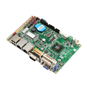
- Page 1 G E N E - C V 0 5 GENE-CV05 ® Intel Atom D2550/N2800/N2600 Processor With LVDS 10/100/1000Base-TXEthernet 1 Mini Card, LPC 6 USB2.0, 6 COM 2CH HD Audio + 2W Amplifier GENE-CV05 Manual Rev. A 7 January 16 , 2014...
-
Page 2: Copyright Notice
AAEON assumes no liabilities resulting from errors or omissions in this document, or from the use of the information contained herein. AAEON reserves the right to make changes in the product design without notice to its users. - Page 3 S u b C o m p a c t B o a r d G E N E - C V 0 5 Acknowledgments All other products’ name or trademarks are properties of their respective owners. AMI is a trademark of American Megatrends Inc. ...
-
Page 4: Packing List
Packing List Before you begin installing your card, please make sure that the following materials have been shipped: ® GENE-CV05 CPU Card with Active Cooler (Intel ® Atom™ D2550 version) or Passive Heatsink (Intel Atom™ N2800/N2600 version) DVD-ROM for manual (in PDF format) and drivers If any of these items should be missing or damaged, please contact your distributor or sales representative immediately. -
Page 5: Table Of Contents
S u b C o m p a c t B o a r d G E N E - C V 0 5 Contents Chapter 1 General Information 1.1 Introduction ..............1-2 1.2 Features ..............1-3 1.3 Specifications ............1-4 Chapter 2 Quick Installation Guide 2.1 Safety Precautions ............ - Page 6 S u b C o m p a c t B o a r d G E N E - C V 0 5 2.17 1st LVDS Operating Voltage Selection (JP11) ..2-13 2.18 Front Panel (CN1) ........... 2-13 2.19 External +5VSB Input (CN2) ........2-13 2.20 CPU Fan Connector (CN3) ........
- Page 7 S u b C o m p a c t B o a r d G E N E - C V 0 5 2.42 Stereo-L Channel (CN25) ........2-22 2.43 1st LVDS Inverter (CN26) ........2-22 2.44 1st LVDS Output-Single Channel 18/24-bit (CN27) 2-22 2.45 2nd RJ-45 Ethernet Connector (CN28) ....
- Page 8 S u b C o m p a c t B o a r d G E N E - C V 0 5 Appendix B I/O Information B.1 I/O Address Map ............ B-2 B.2 1 MB Memory Address Map ........ B-4 B.3 IRQ Mapping Chart ..........
-
Page 9: Chapter 1 General Information
S u b C o m p a c t B o a r d G E N E - C V 0 5 Chapter General Information 1- 1 Chapter 1 General Information... -
Page 10: Introduction
Six USB2.0, six COM Ports (five RS-232, one RS-232/422/485) and 8-bit digital I/O are configured on the GENE-CV05 as well. Full functions make GENE-CV05 user friendly. This brand new SubCompact board is developed to cater to the requirements of Automation, Medical, ticket machine, transportation, gaming, KIOSK, and POS/POI applications. -
Page 11: Features
S u b C o m p a c t B o a r d G E N E - C V 0 5 1.2 Features ® Onboard Intel Atom™ D2550/N2800/N2600 Processor ® Intel NM10 ® DDR3 800/1066 SODIMM , Max. 4 GB for Intel Atom™... -
Page 12: Specifications
S u b C o m p a c t B o a r d G E N E - C V 0 5 1.3 Specifications System ® Processor Intel Atom™ D2550/N2800/N2600 Processor System Memory 204-pin DDR3 SODIMM x 1, Max. - Page 13 S u b C o m p a c t B o a r d G E N E - C V 0 5 Battery Lithium battery Board Size 5.75”(L) x 4”(W) (146mm x 101.6mm) Gross Weight 0.88 lb (0.4 Kg) ...
- Page 14 Supports 4/5/8-wire resistive touch screen Note: (1) If you choose Parallel Port, the COM6 will be removed from the GENE-CV05. (2) Dose not support RC-D (2Rx16 dual die), and RC-E(2Rx16) DDR3 SODIMM momery. (3) Max memory size by sku: N2600 series 2GB; N2800,...
- Page 15 S u b C o m p a c t B o a r d G E N E - C V 0 5 D2550 series 4GB. 1 - 7 Chapter 1 General Information...
-
Page 16: Chapter 2 Quick Installation Guide
S u b C o m p a c t B o a r d G E N E - C V 0 5 Chapter Quick Installation Guide Chapter 2 Quick Installation Guide... -
Page 17: Safety Precautions
S u b C o m p a c t B o a r d G E N E - C V 0 5 2.1 Safety Precautions Always completely disconnect the power cord from your board whenever you are working on it. -
Page 18: Location Of Connectors And Jumpers
S u b C o m p a c t B o a r d G E N E - C V 0 5 2.2 Location of Connectors and Jumpers Component Side Chapter 2 Quick Installation Guide... -
Page 19: Solder Side
S u b C o m p a c t B o a r d G E N E - C V 0 5 Solder Side Chapter 2 Quick Installation Guide... -
Page 20: Mechanical Drawing
S u b C o m p a c t B o a r d G E N E - C V 0 5 2.3 Mechanical Drawing Component Side Chapter 2 Quick Installation Guide... - Page 21 S u b C o m p a c t B o a r d G E N E - C V 0 5 Solder Side Chapter 2 Quick Installation Guide...
-
Page 22: List Of Jumpers
S u b C o m p a c t B o a r d G E N E - C V 0 5 2.4 List of Jumpers The board has a number of jumpers that allow you to configure your system to suit your application. -
Page 23: List Of Connectors
S u b C o m p a c t B o a r d G E N E - C V 0 5 2.5 List of Connectors The board has a number of connectors that allow you to configure your system to suit your application. - Page 24 S u b C o m p a c t B o a r d G E N E - C V 0 5 CN19 COM Port #2 CN20 Touch Screen CN21 Stereo-R Channel CN22 LVDS (Dual channel 18/24bit) CN23 PS/2 Keyboard &...
-
Page 25: Setting Jumpers
S u b C o m p a c t B o a r d G E N E - C V 0 5 2.6 Setting Jumpers You configure your card to match the needs of your application by setting jumpers. A jumper is the simplest kind of electric switch. It consists of two metal pins and a small metal clip (often protected by a plastic cover) that slides over the pins to connect them. -
Page 26: Auto Power Button Selection (Jp1)
S u b C o m p a c t B o a r d G E N E - C V 0 5 2.7 Auto Power Button Selection (JP1) Function Enable(Default) Disable 2.8 Clear CMOS (JP2) Function Normal (Default) Clear CMOS 2.9 COM2 RI/+5V/+12V Selection (JP3) Function... -
Page 27: 2Nd Lvds Backlight Bias/Pwm Mode Selection (Jp6)
S u b C o m p a c t B o a r d G E N E - C V 0 5 2.12 2 LVDS Backlight Bias/PWM Mode Selection (JP6) Function Bias (Default) PWM Control 2.13 2 LVDS Operating Voltage Selection (JP7) Function +3.3V (Default) Note: Max. -
Page 28: 1St Lvds Operating Voltage Selection (Jp11)
S u b C o m p a c t B o a r d G E N E - C V 0 5 2.17 1 LVDS Operating Voltage Selection (JP11) JP11 Function +3.3V (Default) Note: Max. Current rating is 2A. 2.18 Front Panel (CN1) Signal (-) 1-2 (+) -
Page 29: 5Vsb Output W/Smbus (Cn4)
S u b C o m p a c t B o a r d G E N E - C V 0 5 2.21 +5VSB Output w/SMBUS (CN4) Signal SMBDATA Ground SMBCLK Ground PSON# +5 Volt. Standby 2.22 SATA Port (CN5) Signal Ground TX0+... -
Page 30: Digital I/O Connector (Cn7)
S u b C o m p a c t B o a r d G E N E - C V 0 5 2.24 Digital I/O Connector (CN7) I2C Address: 0x6Eh Signal Signal Port 1 Port 2 Port 3 Port 4 Port 5 Port 6... -
Page 31: Output For Sata Hdd Usage (Cn9)
S u b C o m p a c t B o a r d G E N E - C V 0 5 Ground Ground Ground Ground Ground ACK# Ground BUSY Ground Ground SLCT 2.26 +5V Output for SATA HDD Usage (CN9) Signal +5 Volt. -
Page 32: Usb Port #5 (Cn12)
S u b C o m p a c t B o a r d G E N E - C V 0 5 CTSF DTRF Ground 2.29 USB Port #5 (CN12) Signal +5 Volt. Standby Data4- Data4+ Ground Ground 2.30 COM Port #5 (CN13) Signal Signal... -
Page 33: Usb Port #3 (Cn15)
S u b C o m p a c t B o a r d G E N E - C V 0 5 2.32 USB Port #3 (CN15) Signal +5 Volt. Standby Data2- Data2+ Ground Ground 2.33 COM Port #4 (CN16) Signal Signal DCDD... -
Page 34: Com Port #3 (Cn18)
S u b C o m p a c t B o a r d G E N E - C V 0 5 LDRQ#0 LDRQ#1 SERIRQ 2.35 COM Port #3 (CN18) Signal Signal DCDC DSRC RTSC CTSC DTRC Ground 2.36 COM Port #2 (CN19) RS-232 Mode Signal... -
Page 35: Touch Screen (Cn20)
S u b C o m p a c t B o a r d G E N E - C V 0 5 RS-485 Mode Signal Signal TXD- TXD+ N/C / +5 Volt. / (+12 Volt.) Ground 2.37 Touch Screen (CN20) 8-wire Signal 4-wire Signal 5-wire Signal... -
Page 36: Ps/2 Keyboard And Mouse Connector (Cn23)
S u b C o m p a c t B o a r d G E N E - C V 0 5 LCD Volt. Ground LB_CLK# LB_CLK LCD Volt. Ground LB_DATA#_0 LB_DATA_0 LB_DATA#_1 LB_DATA_1 LB_DATA#_2 LB_DATA_2 LB_DATA#_3 LB_DATA_3 LVD_DDCDAT LVD_DDCCLK LC_DATA#_0... -
Page 37: Stereo-L Channel (Cn25)
S u b C o m p a c t B o a r d G E N E - C V 0 5 2.42 Stereo-L Channel Inverter (CN25) Signal 2.43 1 LVDS Inverter (CN26) Signal +5 Volt. / +12 Volt. Brightness Control (Controlled by Cedarview) Ground Ground... -
Page 38: Usb Port #1 And #2 (Cn30)
S u b C o m p a c t B o a r d G E N E - C V 0 5 LCD Volt. Ground 2.45 2 RJ-45 Ethernet Connector (CN28) Signal Signal LAN2_MDIO0+ LAN2_MDIO0- LAN2_MDIO1+ LAN2_MDIO1- LAN2_TCD0 LAN2_TCD1 LAN2_MDIO2+ LAN2_MDIO2-... -
Page 39: Audio Line In/Out And Mic (Cn31)
S u b C o m p a c t B o a r d G E N E - C V 0 5 Data0+ Data1+ Ground Ground 2.48 Audio Line In/Out and MIC (CN31) Signal MIC_L MIC_R Ground Line IN_L Line IN_R Ground Line OUT_L... -
Page 40: Com Port #1 (Cn33)
S u b C o m p a c t B o a r d G E N E - C V 0 5 Ground +5 Volt. Ground DVI_DET DVI_TDC0# DVI_TDC0 Ground Ground DVI_TLC DVI_TLC# Ground Ground CRT Display Signal Signal DDCCLK +5 Volt. -
Page 41: Sim Card Socket (Cn34)
S u b C o m p a c t B o a r d G E N E - C V 0 5 2.51 SIM Card Socket (CN34) Signal Signal UIM_PWR UIM_RST UIM_CLK Ground UIM_VPP UIM_DATA 2.52 CFast™ Disk (CFD1) Signal Ground SATA_TX+... -
Page 42: Mini Card/ Msata (Pcie1)
S u b C o m p a c t B o a r d G E N E - C V 0 5 +3.3 Volt. +3.3 Volt. Ground Ground 2.53 Mini Card/ mSATA (PCIE1) Signal Signal +3.3 Volt. Standby/+3.3 PCIE_WAKE# Volt. -
Page 43: Ddr3 Sodimm Slot (Dimm1)
S u b C o m p a c t B o a r d G E N E - C V 0 5 +3.3 Volt. Standby/+3.3 Ground Volt. +3.3 Volt. Standby/+3.3 Volt. Ground +1.5 Volt. Ground +3.3 Volt. Standby/+3.3 Volt. - Page 44 S u b C o m p a c t B o a r d G E N E - C V 0 5 Below Table for China RoHS Requirements 产品中有毒有害物质或元素名称及含量 AAEON Main Board/ Daughter Board/ Backplane 有毒有害物质或元素 部件名称 铅...
-
Page 45: Chapter 3 Ami Bios Setup
S u b C o m p a c t B o a r d G E N E - C V 0 5 Chapter BIOS Setup Chapter 3 AMI BIOS Setup 3-1... -
Page 46: System Test And Initialization
3. The CMOS memory has lost power and the configuration information has been erased. The GENE-CV05 CMOS memory has an integral lithium battery backup for data retention. However, you will need to replace the complete unit when it runs down. -
Page 47: Ami Bios Setup
S u b C o m p a c t B o a r d G E N E - C V 0 5 3.2 AMI BIOS Setup AMI BIOS ROM has a built-in Setup program that allows users to modify the basic system configuration. - Page 48 S u b C o m p a c t B o a r d G E N E - C V 0 5 2. If the "Control LVDS2 (CH7511)" has been set "Enable," and then, the screen can be switched to LVDS2 under the OS. 3.
-
Page 49: Setup Menu
S u b C o m p a c t B o a r d G E N E - C V 0 5 Setup Menu Setup submenu: Main Options summary: (default setting) System Date Day MM:DD:YYYY Change the month, year and century. The ‘Day’ is changed automatically. System Time HH : MM : SS Change the clock of the system. - Page 50 S u b C o m p a c t B o a r d G E N E - C V 0 5 Setup submenu: Advanced Options summary: (default setting) ACPI Settings System ACPI Parameters S5 RTC Wake Settings Support S5 RTC Wake Function Trusted Computing TPM Function...
- Page 51 S u b C o m p a c t B o a r d G E N E - C V 0 5 Dynamic Digital IO Configuration Digital IO Configuration SATA Configuration SATA Device Options Settings USB Configuration USB Configuration Parameters Super IO Configuration IT8783 Super IO Configuration Parameters H/W Monitor...
-
Page 52: Acpi Settings
S u b C o m p a c t B o a r d G E N E - C V 0 5 ACPI Settings Options summary: (default setting) Suspend Disabled ACPI Sleep State S3 (Suspend to RAM) Select the ACPI state used for System Suspend Chapter 3 AMI BIOS Setup 3-8... -
Page 53: S5 Rtc Wake Settings
S u b C o m p a c t B o a r d G E N E - C V 0 5 S5 RTC Wake Settings Options summary: (default setting) Wake system with Fixed Disabled Time Enabled Enable or disable System wake on alarm event. Wake up time is setting by following settings. - Page 54 S u b C o m p a c t B o a r d G E N E - C V 0 5 Wake up minute 0-59 Wake up second 0-59 Wake system with Disabled Dynamic Time Enabled Enable or disable System wake on alarm event. Wake up time is current time + Increase minutes.
-
Page 55: Trusted Computing
S u b C o m p a c t B o a r d G E N E - C V 0 5 Trusted Computing Security Device Support Disabled Enabled Enable or disable TPM Chapter 3 AMI BIOS Setup 3-11... -
Page 56: Cpu Configuration
S u b C o m p a c t B o a r d G E N E - C V 0 5 CPU Configuration Options summary: (default setting) Hyper-Threading Disabled Enabled CPU Hyper-Threading Technology support or not Chapter 3 AMI BIOS Setup 3-12... - Page 57 S u b C o m p a c t B o a r d G E N E - C V 0 5 Dynamic Digital IO Configuration Digital Port x(GP2x) Input Direction Output Digital Port Direction Digital Port x(GP2x) Level Digital Port Level Chapter 3 AMI BIOS Setup 3-13...
-
Page 58: Sata Configuration
S u b C o m p a c t B o a r d G E N E - C V 0 5 SATA Configuration Options summary: (default setting) SATA Controller(s) Enabled Disabled SATA Controller Enable/Disable SATA Mode AHCI Configure SATA controller operating as IDE/AHCI mode. -
Page 59: Usb Configuration
S u b C o m p a c t B o a r d G E N E - C V 0 5 SATA Portx Hot Plug Enabled Disabled Enable / Disable SATA Portx Hot Plug function USB Configuration Options summary: (default setting) Legacy USB Support Enabled... -
Page 60: Super Io Configuration
S u b C o m p a c t B o a r d G E N E - C V 0 5 no USB devices are connected. DISABLE option will keep USB devices available only for EFI application Device Name Auto (Emulation Type) - Page 61 S u b C o m p a c t B o a r d G E N E - C V 0 5 Options summary: (default setting) Serial Port x Configuration Set Parameters of Serial Port x Parallel Port Configuration Set Parallel Port Configuration Restore AC Power Loss Power off...
- Page 62 S u b C o m p a c t B o a r d G E N E - C V 0 5 Options summary: (default setting) Serial Port Disabled Enabled En/Disable specified serial port. Change Settings Auto IO=2F8h; IRQ=3; IO=3F8h;...
- Page 63 S u b C o m p a c t B o a r d G E N E - C V 0 5 Parallel Port Configuration Parallel Port Disabled Enabled En/Disable specified Parallel port. Change Settings Auto IO=378h; IRQ=5; IO=378h;...
- Page 64 S u b C o m p a c t B o a r d G E N E - C V 0 5 IO=3BCh; Select a resource setting for Super IO device. Device Mode Standard Parallel Port Mode EPP Mode ECP Mode EPP Mode &...
- Page 65 S u b C o m p a c t B o a r d G E N E - C V 0 5 Manual Mode Smart Fan 1 Mode Select H/W Monitor Chapter 3 AMI BIOS Setup 3-21...
- Page 66 S u b C o m p a c t B o a r d G E N E - C V 0 5 Setup submenu: Chipset Options summary: (default setting) Host Bridge Host Bridge Parameters South Bridge South Bridge Parameters Chapter 3 AMI BIOS Setup 3-22...
-
Page 67: Host Bridge
S u b C o m p a c t B o a r d G E N E - C V 0 5 Host Bridge Options summary: (default setting) Intel IGD Configuration Enter to set Graphic Configuration Memory Information Show current memory information Chapter 3 AMI BIOS Setup 3-23... -
Page 68: Intel Igd Configuration
S u b C o m p a c t B o a r d G E N E - C V 0 5 Intel IGD Configuration Options summary: (default setting) Auto Disable IGD Disabled Enabled IGFX – Boot Type VBIOS Default LVDS CRT + 1... - Page 69 S u b C o m p a c t B o a r d G E N E - C V 0 5 LCD Panel Type 640x480 18bit 800x600 18bit 1024x768 18bit 800x480 18bit 1366x768 18bit 1280x768 18bit 640x480 24bit (D2550 CPU only) 800x600 24bit (D2550 CPU only)
- Page 70 S u b C o m p a c t B o a r d G E N E - C V 0 5 1024x768 24bit 1280x1024 48bit 1280x768 24bit 1366x768 24bit 1440x900 48bit 1600x1200 48bit 1920x1080 48bit (D2550 CPU only) 1920x1200 48bit (D2550 CPU only) Select 2...
-
Page 71: South Bridge
S u b C o m p a c t B o a r d G E N E - C V 0 5 Size 256MB Configure Fixed Graphics Memory Size South Bridge Options summary: (default setting) Power Mode Select AT/ATX Power Mode TPT Devices Configure onboard TPT Devices PCI Express Port x... - Page 72 S u b C o m p a c t B o a r d G E N E - C V 0 5 Enable/Disable PCI Express Port 0 - 3 TPT Devices Options summary: (default setting) Azalia Controller Disabled HD Audio Azalia Controller Enable/Disable R8111E #x Controller...
- Page 73 S u b C o m p a c t B o a r d G E N E - C V 0 5 R8111E Enable/Disable Chapter 3 AMI BIOS Setup 3-29...
-
Page 74: Boot Configuration
S u b C o m p a c t B o a r d G E N E - C V 0 5 Boot Configuration Options summary: (default setting) Quiet Boot Disabled Enabled Enables or disables Quiet Boot option Launch 8111E PXE Disabled OpROM... - Page 75 S u b C o m p a c t B o a r d G E N E - C V 0 5 BBS Priorities Options summary: (default setting) Boot Option #x Disabled Device name Sets the system boot order Chapter 3 AMI BIOS Setup 3-31...
- Page 76 S u b C o m p a c t B o a r d G E N E - C V 0 5 Setup submenu: Security Options summary: (default setting) Administrator Password/ Not set User Password You can install a Supervisor password, and if you install a supervisor password, you can then install a user password.
- Page 77 S u b C o m p a c t B o a r d G E N E - C V 0 5 required at boot time, or when the user enters the Setup utility. Removing the Password: Highlight this item and type in the current password. At the next dialog box press Enter to disable password protection.
- Page 78 S u b C o m p a c t B o a r d G E N E - C V 0 5 entered while system booting. Install the Password: Press Enter on this item, a dialog box appears which lets you enter a password. You can enter no more than six letters or numbers.
- Page 79 S u b C o m p a c t B o a r d G E N E - C V 0 5 Options summary: (default setting) Save Changes and Reset Reset the system after saving the changes Discard Changes and Reset Reset system setup without saving any changes Restore Defaults Restore/Load Default values for all the setup options.
-
Page 80: Chapter 4 Driver Installation
S u b C o m p a c t B o a r d G E N E - C V 0 5 Chapter Driver Installation Chapter 4 Driver Installation... - Page 81 S u b C o m p a c t B o a r d G E N E - C V 0 5 The GENE-CV05 comes with a DVD-ROM that contains all drivers and utilities that meet your needs.
- Page 82 S u b C o m p a c t B o a r d G E N E - C V 0 5 4.1 Installation: Insert the GENE-CV05 DVD-ROM into the DVD-ROM Drive. And install the drivers from Step 1 to Step 8 in order. Step 1 – Install Chipset Driver 1.
- Page 83 S u b C o m p a c t B o a r d G E N E - C V 0 5 Follow the instructions that the window shows The system will help you install the driver automatically Chapter 4 Driver Installation...
- Page 84 S u b C o m p a c t B o a r d G E N E - C V 0 5 Chapter4 Drivers Installation...
- Page 85 S u b C o m p a c t B o a r d G E N E - C V 0 5 If you want to update driver, please uninstall driver first. Uninstall IEMGD 1. Double click on the IEMGDInstall.exe 2.
- Page 86 S u b C o m p a c t B o a r d G E N E - C V 0 5 2. Double click on the Setup.exe file located in each OS folder 3. Follow the instructions that the window shows 4.
- Page 87 S u b C o m p a c t B o a r d G E N E - C V 0 5 Double click on the Serial Patch v1.0.1_Eng.exe file located in each OS folder Follow the instructions that the window shows The system will help you install the driver automatically Note: If the OS is Chinese version, you may click on Serial Patch v1.0.1.
-
Page 88: Appendix A Programming The Watchdog Timer
S u b C o m p a c t B o a r d G E N E - C V 0 5 Appendix Programming the Watchdog Timer Appendix A Programming the Watchdog Timer A-1... -
Page 89: Programming
S u b C o m p a c t B o a r d G E N E - C V 0 5 A.1 Programming GENE-CV05 utilizes ITE 8783 chipset as its watchdog timer controller. Below are the procedures to complete its configuration and the AAEON initial watchdog timer program is also attached based on which you can develop customized program to fit your application. - Page 90 S u b C o m p a c t B o a r d G E N E - C V 0 5 There are three steps to complete the configuration setup: (1) Enter the MB PnP Mode; (2) Modify the data of configuration registers; (3) Exit the MB PnP Mode.
- Page 91 S u b C o m p a c t B o a r d G E N E - C V 0 5 WatchDog Timer Configuration Registers Configure Control (Index=02h) This register is write only. Its values are not sticky; that is to say, a hardware reset will automatically clear the bits, and does not require the software to clear them.
- Page 92 S u b C o m p a c t B o a r d G E N E - C V 0 5 Watch Dog Timer 1, 2, 3 Configuration Register (Index=72h, 82h, 92h Default=001s0000b) Watch Dog Timer 1,2,3 Time-Out Value (LSB) Register (Index=73h,83h,93h, Default=38h) Watch Dog Timer 1,2,3 Time-Out Value (MSB) Register (Index=74h,84h,94h Default=00h)
-
Page 93: A.2 Ite8783 Watchdog Timer Initial Program
S u b C o m p a c t B o a r d G E N E - C V 0 5 A.2 ITE8783 Watchdog Timer Initial Program .MODEL SMALL .CODE Main: CALL Enter_Configuration_mode CALL Check_Chip mov cl, 7 call Set_Logic_Device ;time setting mov cl, 10 ;... - Page 94 S u b C o m p a c t B o a r d G E N E - C V 0 5 call Superio_Set_Reg ; game port enable mov cl, 9 call Set_Logic_Device Initial_OK: CALL Exit_Configuration_mode MOV AH,4Ch INT 21h Enter_Configuration_Mode PROC NEAR MOV SI,WORD PTR CS:[Offset Cfg_Port]...
- Page 95 S u b C o m p a c t B o a r d G E N E - C V 0 5 CALL Write_Configuration_Data Exit_Configuration_Mode ENDP Check_Chip PROC NEAR MOV AL,20h CALL Read_Configuration_Data CMP AL,87h JNE Not_Initial MOV AL,21h CALL Read_Configuration_Data CMP AL,81h JNE Not_Initial...
- Page 96 S u b C o m p a c t B o a r d G E N E - C V 0 5 OUT DX,AL MOV DX,WORD PTR CS:[Cfg_Port+06h] IN AL,DX Read_Configuration_Data ENDP Write_Configuration_Data PROC NEAR MOV DX,WORD PTR CS:[Cfg_Port+04h] OUT DX,AL XCHG AL,AH MOV DX,WORD PTR CS:[Cfg_Port+06h]...
- Page 97 S u b C o m p a c t B o a r d G E N E - C V 0 5 Set_Logic_Device proc near push ax push cx xchg al,cl mov cl,07h call Superio_Set_Reg pop cx pop ax Set_Logic_Device endp ;Select 02Eh->Index Port, 02Fh->Data Port Cfg_Port DB 087h,001h,055h,055h...
- Page 98 S u b C o m p a c t B o a r d G E N E - C V 0 5 Appendix I/O Information B - 1 Appendix B I/O Information...
-
Page 99: B.1 I/O Address Map
S u b C o m p a c t B o a r d G E N E - C V 0 5 B.1 I/O Address Map B - 2 Appendix B I/O Information... - Page 100 S u b C o m p a c t B o a r d G E N E - C V 0 5 B - 3 Appendix B I/O Information...
- Page 101 S u b C o m p a c t B o a r d G E N E - C V 0 5 B.2 1 MB Memory Address Map B - 4 Appendix B I/O Information...
-
Page 102: B.3 Irq Mapping Chart
S u b C o m p a c t B o a r d G E N E - C V 0 5 B.3 IRQ Mapping Chart B - 5 Appendix B I/O Information... -
Page 103: B.4 Dma Channel Assignments
S u b C o m p a c t B o a r d G E N E - C V 0 5 B.4 DMA Channel Assignments B - 6 Appendix B I/O Information... - Page 104 S u b C o m p a c t B o a r d G E N E - C V 0 5 Appendix Mating Connector C - 1 Appendix C Mating Connector...
-
Page 105: C.1 List Of Mating Connectors And Cables
S u b C o m p a c t B o a r d G E N E - C V 0 5 C.1 List of Mating Connectors and Cables The table notes mating connectors and available cables. Mating Connector Connector Available Cable P/N... - Page 106 S u b C o m p a c t B o a r d G E N E - C V 0 5 Cable LPC Expansion SHR-12V-S AAEON CN17 1703120130 LPC Cable UART Wafer CN18 COM Port #3 Molex...
-
Page 107: Ahci Setting
S u b C o m p a c t B o a r d G E N E - C V 0 5 A ppendix AHCI Setting Appendix D AHCI Setting... -
Page 108: D.1 Setting Ahci
S u b C o m p a c t B o a r d G E N E - C V 0 5 D.1 Setting AHCI OS installation to setup AHCI Mode. Step 1: Copy the files below from “Driver CD -> STEP5-AHCI\WIN7_32\F6 Install Floppy Create for 32 and 64 bit Windows”... - Page 109 S u b C o m p a c t B o a r d G E N E - C V 0 5 Step 3: Setup OS Step 4: Press “F6” Appendix D AHCI Setting...
- Page 110 S u b C o m p a c t B o a r d G E N E - C V 0 5 Step 5: Choose “S” tep 6: Choose “Intel(R) NM10 Express Chipset” Appendix D AHCI Setting...
- Page 111 S u b C o m p a c t B o a r d G E N E - C V 0 5 Step 7: It will show the model number you select and then press “ENTER Step 8: Setup is loading files Appendix D AHCI Setting...
- Page 112 S u b C o m p a c t B o a r d G E N E - C V 0 5 Appendix Digital I/O Appendix E Digital I/O E-1...
-
Page 113: E.1 Digital I/O
S u b C o m p a c t B o a r d G E N E - C V 0 5 E.1 Digital I/O The F75111 provides one serial access interface, I2C Bus, to read/write internal registers. The address of Serial Bus is 0x6E (0110_1110) The related register for configuring DIO is list as follows: Configuration and Control Register-Index 01h Power-on default [7:0]=0000_1000b... - Page 114 S u b C o m p a c t B o a r d G E N E - C V 0 5 GPIO2x Output Control Register-Index 20h Power-on default [7:0]=0000_0000b Name Description GPIO 27 output control. Set to 1 GP27_OCT for output function.
- Page 115 S u b C o m p a c t B o a r d G E N E - C V 0 5 GP24_ODA VSB3V GPIO 24 output data. GP23_ODA GPIO 23 output data. VSB3V GP22_ODA VSB3V GPIO 22 output data. GP21_ODA VSB3V GPIO 21 output data.
- Page 116 S u b C o m p a c t B o a r d G E N E - C V 0 5 begin: cl,01h al,80h call CT_I2CWriteByte call Delay5ms mov al,00h cl,20h call CT_I2CWriteByte cl,22h call CT_I2CReadByte ;Input : CL - register index CH - device ID ;Output : AL - Value read Ct_I2CReadByte...
- Page 117 S u b C o m p a c t B o a r d G E N E - C V 0 5 call Delay5ms dx, 0f000h + 04h ; Transmit Slave Address Register ; Set the slave address and al, ch ;...
- Page 118 S u b C o m p a c t B o a r d G E N E - C V 0 5 Ct_I2CReadByte Endp ;Input : CL - register index CH - device ID AL - Value to write ;Output: none Ct_I2CWriteByte Proc Near...
- Page 119 S u b C o m p a c t B o a r d G E N E - C V 0 5 dx, al dx, 0f000h + 05h al, ah dx, al dx, 0f000h + 00h ; Host Control Register al, 48h ;...
- Page 120 S u b C o m p a c t B o a r d G E N E - C V 0 5 dx,al ;clear status call Delay5ms test al, 02H ;termination of command ? short Clear_final al, NOT 40H ;mask INUSE bit al,al ;status OK ? short Clear_final...
Need help?
Do you have a question about the GENE-CV05 and is the answer not in the manual?
Questions and answers