Sign In
Upload
Manuals
Brands
Tektronix Manuals
Test Equipment
2246 2R
Tektronix 2246 2R Manuals
Manuals and User Guides for Tektronix 2246 2R. We have
1
Tektronix 2246 2R manual available for free PDF download: Service Manual
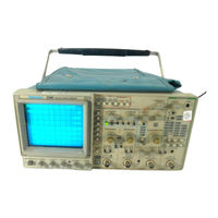
Tektronix 2246 2R Service Manual (433 pages)
PORTABLE OSCILLOSCOPE
Brand:
Tektronix
| Category:
Test Equipment
| Size: 49.17 MB
Table of Contents
Table of Contents
4
List of Illustrations
9
Operators Safety Summary
11
Servicing Safety Summary
12
Specification
14
Introduction
14
Standard Accessories
14
Recommended Recalibration Schedule
14
Portable Oscilloscope
14
Performance Conditions
15
Environmental C Haracteristics
15
Electrical Characteristics
16
Maximum Input Voltage Vs Frequency
27
Mechanical Characteristics
30
Dimensional Outline Drawing, Standard Cabinet
33
Dimensional Outline Drawing
34
Preparation for Use
36
Safety
36
Line Voltage and Power Cord
36
Line Fuse
36
Instrument Cooling
37
Start-Up
37
Detailed Operating Information
37
Theory of Operation
38
Section Organization
38
Integrated Circuit Descriptions
38
Block Diagram Description
38
Introduction
38
Vertical Inputs
38
Block Diagram
38
Vertical Preamps and Output Amplifier
39
A and B Trigger System
39
Display and Trigger Logic and Processor Interface
40
(Diagram 4)
40
A and B SWEEPS and DELAY COMPARATORS (Diagram 5)
41
HORIZONTAL OUTPUT AMPLIFIER (Diagram 6 )
41
Z-AXIS, CRT, PROBE ADJUST, and CONTROL MUX (Diagram 7)
41
MEASUREMENT PROCESSOR (Diagram 8)
42
READOUT SYSTEM (Diagram 9)
42
SWITCH BOARD and INTERFACE (Diagram 10)
43
ADC and DAC SYSTEM (Diagram 11)
43
POWER SUPPLY (Diagram 12)
43
Detailed Circuit Description
43
Vertical Inputs
43
(Diagram 1)
43
Shift Register 0 Bit Assignment
44
AMPLIFIER (Diagram 2 )
45
Input Coupling Control Bit States
45
CH 1 and CH 2 Attenuator and Gain Control Bit States
46
CH 2 INVERT Control Bit
46
CH 3 and CH 4 Gain Control Bit
47
A and B TRIGGER SYSTEM (Diagram 3)
49
Trigger Selection Logic
50
(Diagram 4)
52
Display Sequencer 1C (SLIC, U600)
53
Pin-Out D Ia G Ra M
53
Display Sequencer (U600) Control Bit Assignments
55
A Trigger Source Select Bits
56
Horizontal Display Mode Select Bits
56
Shift Register 1 Control Bit Data
57
Trigger Source Select
58
Vertical MODE Select
58
Horizontal MODE Select
58
Holdoff Counter Encoding
59
Display Sequencer Channel Select Logic Bits
60
Horizontal and Vertical Display Response
61
Readout Interface Relative
62
Trigger Logic 1C (FLIC, U602)
63
Pin-Out Diagram
63
Control Register Signal-Bit Names
65
Delay Mode Selection Control Bits
65
Peak Volts Detection Mode Logic
65
Z-Axis Switching Logic
67
A and B SWEEPS and DELAY COMPARATORS (Diagram 5)
68
A Sweep Timing Selections
71
B Sweep Timing Selections
72
A Sweep Start Circuit Waveforms
73
HORIZONTAL OUTPUT AMPLIFIER (Diagram 6)
74
Z-AXIS, CRT, PROBE ADJUST, and CONTROL MUX (Diagram 7)
75
Simplified Diagram of the DC Restorer Circuitry
77
Front-Panel Multiplexer Channel Select Bits
78
MEASUREMENT PROCESSOR (Diagram 8)
79
Measurement Processor Signals
80
READOUT SYSTEM (Diagram 9)
82
Display Addresses
85
Position Enable Bit Assignment
86
Character Pixel Arrangement
87
Field and Mixer Attribute Bit Assignment
87
SWITCH BOARD and INTERFACE (Diagram 10)
88
Display Possibilities
88
Possible Signal Conditions
88
ADC and DAC SYSTEM (Diagram 11)
89
POWER SUPPLY (Diagram 12)
90
Power Supply Block Diagram
91
MAIN BOARD POWER DISTRIBUTION (Diagram 13)
95
Processor Power Board
95
DISTRIBUTION (Diagram 14)
95
INTERCONNECTION DIAGRAM (Diagram 15)
95
Performance Check Procedure
96
Introduction
96
Test Equipment Required
96
Performance Check Interval
96
Preparation
96
Test Equipment Required
97
Index to Performance Check Procedure
99
Display
100
Trace Rotation
100
Geometry
100
G Eo M E Try
100
Vertical
101
Input COUPLING Functional Check
101
CH 1 and CH 2 VOLTS/DIV Trace Shift
101
CH 1 and CH 2 VOLTS/DIV Trace S H Ift
101
CH 3 and CH 4 VOLTS/DIV Trace Shift
102
CH 3 and CH 4 VOLTS/DIV Trace S H Ift
102
CH 1 and CH 2 VAR VOLTS/DIV Trace Shift
102
CH 1 and CH 2 Input COUPLING Trace Shift
102
CH 2 INVERT Trace Shift
102
CH 1 and CH 2 VAR VOLTS/DIV Range
102
CH 1 and CH 2 VAR VOLTS/DIVR Ange
102
Low-Frequency Linearity
103
CH 1 and CH 2 Vertical Deflection Accuracy
103
CH 3 and CH 4 Vertical Deflection Accuracy
103
S Ignal-To-G Raticule Accuracy
103
ADD Mode and CH 2 INVERT Deflection Accuracy
104
Vertical POSITION Range (All Channels)
104
CH 1 to CH 2 Signal Delay Match
105
CH 1 to CH 4 Signal Delay Match
105
CH 3 to CH 4 Signal Delay Match
105
CH 1 and CH 2 Vertical Bandwidth
105
CH 3 and CH 4 Vertical Bandwidth
106
CH 1 and CH 2 Aberrations
106
CH 1 and CH 2 a be Rratio N S
106
SCOPE BW (Bandwidth Limit) Accuracy
106
Common-Mode Rejection Ratio
107
Channel Isolation
107
AC-Coupled Lower -3 Db Point
108
Vertical ALT and CHOP Modes
108
BEAM FIND Functional Check
108
A and B Trace Separation
108
A and B Trace S E P a Ra Tio N
108
S E N S Itiv Ity
109
Triggering
109
Hz Trigger Sensitivity
109
S E N S Itiv Ity
110
Khz Trigger Sensitivity
110
Mhz Trigger Sensitivity
110
Trigger Sensitivity
111
Single Sweep Mode
111
Trigger LEVEL Control Range
111
Mhz NOISE REJ Trigger Sensitivity
111
TV Field Trigger Sensitivity
112
TV Line Trigger Sensitivity
112
Line Trigger Functional Check
112
Horizontal
113
A and B Sweep Length
113
Horizontal POSITION Range
113
VAR SEC/DIV Range
113
Magnifier Registration
114
Magnifier R E G Istratio N
114
A and B Timing Accuracy and Linearity
114
A and B Magnified Timing Accuracy
114
Delay Time Jitter
115
Delay Time J It T E R
115
Settings for Timing Accuracy Checks
115
Delay Time Accuracy
116
Delay Time a C C U Ra C y
116
Delay Time Position Range
116
X-Axis Gain Accuracy
116
Y Phase Difference
117
X-Axis Bandwidth
117
Time and Cursors Measurements
118
Cursor Accuracy
118
Delta Time Accuracy
118
Accuracy
118
K- Phase -H Cursor a C C U Ra C y
119
K- VOLTS -H Cursor a C C U Ra C y
119
Tracking Cursors Position Accuracy
119
K- VOLTS-* Cursor Accuracy
119
Ch1/Ch2 Voltmeter Measurements
120
DC Volts Accuracy
120
DC Volts Normal Mode Rejection Ratio
120
Peak, -Peak, Peak-To-Peak Volts Accuracy
121
Accuracy
121
Gated Volts Accuracy
121
Gated Volts a C C U Ra C y
121
Peak, - Peak, and Peak-To-Peak Volts Accuracy
121
Mhz +Peak, - Peak, and Peak-To-Peak Volts Accuracy
121
Peak-To-Peak Volts a C C U Ra C y
121
External Z-Axis, Probe Adjust and Front-Panel Setup Functions
123
Check External Z-Axis Input
123
PROBE ADJUST Output
123
Run MAKE FACTORY SETTINGS Routine
123
Run MAKE FACTORY SETTINGSR O U Tin E
123
Adjustment Procedure
124
Introduction
124
Purpose
124
Test Equipment Required
124
Limits and Tolerances
124
Partial Procedures
124
Internal Adjustments and Adjustment Interaction
124
Adjustment Interactions
125
Preparation for Adjustment
126
Index to Adjustment Procedure
126
Power Supply, Display, and Z-Axis
127
Initial Control Settings
127
Procedure
127
Power Supply DC Levels (R2252)
127
Grid Bias (R2719)
128
Astigmatism (R 2788)
128
Astigmatism (R2788)
128
Trace Rotation (Front Panel)
128
Geometry (R 2 7 84 )
128
Geometry (R2784)
128
Pow er Supply Voltage Limits
128
Z-Axis Response (C2704)
128
Readout Jitter (R724)
129
Vertical
130
Initial Control Settings
130
Procedure
130
Vertical Output Gain (R703) and Readout Vertical Centering (R260)
130
Vertical Output Gain (R703) and Readout Vertical Centering (R 2 6 0 )
130
CH 1 Step Balance (R12)
130
CH 2 Step Balance (R22)
131
CH 3 Step Balance (R141)
131
CH 4 Step Balance (R161)
131
CH 1 MF/LF Gain (R13) and Compensation (C L)
131
CH 1 MF/LF Gain (R13) and Compensation ( C L )
131
CH 1 Input Capacitance (Cl 14)
131
CH 1 Input Capacitance (Cl 1 4 )
131
CH 1 Input Compensation X I 0 (C 1 1 )
131
CH 1 Input Compensation X I 00 ( C IO )
131
CH 1 Input Compensation X I 00 (CIO)
131
CH 2 Input Capacitance (Cl 24)
132
CH 2 Input Capacitance ( C L2 4 )
132
CH 2 Input Compensation X I 0 (C21)
132
CH 2 Input Compensation X I 00 (C 2 0 )
132
CH 2 Input Compensation X I 00 (C20)
132
CH 2 Gain (R221)
132
CH 3 MF/LF Compensation (Cl 3 4 )
132
CH 3 MF/LF Compensation ( C L34)
132
CH 3 Gain (R231)
132
CH 4 MF/LF Compensation (Cl 5 4 )
132
Delay-Line HF Compensation (R272, R273, R275, C274, C273)
133
CH 3 HF Compensation
133
CH 4 HF Compensation
133
CH 1 and CH 2 Bandwidth Check
133
CH 1 and CH 2 Bandwidth C H E C K
133
Areas of Waveform Affected by
133
HF Compensation
133
CH 3 and CH 4 Bandwidth Check
134
CH 3 and CH 4 Bandwidth C H E C K
134
Horizontal
135
Initial Control Settings
135
Procedure
135
H Orizontal X I Gain (Timing) (R 826)
135
Horizontal X I 0 Gain (Timing) (R825)
135
Horizontal X I 0 Gain (Timing) (R 825)
135
Readout Horizontal Gain (R823) and MAG Registration (R809)
135
A 0.5 P.s Timing (C314)
136
Ns Timing (C807, C814)
136
Gain (R827)
136
Measurement Bandwidth and Self Characterization
137
Initial Control Settings
137
Procedure
137
Volts Cal (R920)
137
B Trigger Bandwidth (R455)
137
Self Characterization
137
Maintenance
140
Static-Sensitive Components
140
Relative Susceptibility to Static-Discharge D a M a G E
140
Preventive Maintenance
141
Introduction
141
Inspection and Cleaning
141
External Inspection Checklist
142
Internal Inspection Checklist
142
Lubrication
143
Semiconductor Checks
143
Periodic Readjustment
143
Troubleshooting
144
Introduction
144
Troubleshooting Aids
144
Troubleshooting Equipment
145
Troubleshooting Techniques
145
Power Supply Voltage and Ripple Limits
147
Internal Testing Capabilities
149
Service Mode
150
Initial SERVICE MENU
150
SERVICE MENU with DIAGNOSE
151
Choice Selected
151
SERVICE MENU Selections
151
Diagnose Routines
155
Troubleshooting Hints by Diagram
158
Horizontal Display State Logic
161
Measurement Processor I/O Memory M a P
162
Troubleshooting Measurement Errors
164
Measurement Error Troubleshooting Hints
165
Corrective Maintenance
173
Introduction
173
Maintenance Precautions
173
Obtaining Replacement Parts
173
Repackaging for Shipment
174
Maintenance Aids
174
Interconnections
174
Maintenance Aids
175
Battery
176
Transistors and Integrated Circuits
176
Soldering Techniques
176
Removal and Replacement Instructions
177
Introduction
186
International Power Cords
186
Option 1R Rackmounted Instrument
186
Replaceable Electrical Parts
188
(2246 Mod A)
203
(2246 Mod A)
207
Semiconductor Lead Configurations
274
Locating Components on Schematic Diagrams and Circuit Board Illustrations
275
Signal Line Locations
280
A9-2 MV Bandwidth Board for SN B700100
312
A8-CRT Control Board
356
A16-Processor Board
368
A14-Switch Board
378
A12-Potentiometer Board
385
A18-Power Supply Board
393
Main Board
399
Ns TIMING
409
Advertisement
Advertisement
Related Products
Tektronix 2246 1Y
Tektronix 2246 MOD A
Tektronix 2247A
Tektronix 2245A
Tektronix 2246
Tektronix 2235
Tektronix 222PS
Tektronix 2213A
Tektronix 2221A
Tektronix 221
Tektronix Categories
Test Equipment
Measuring Instruments
Printer
Amplifier
Portable Generator
More Tektronix Manuals
Login
Sign In
OR
Sign in with Facebook
Sign in with Google
Upload manual
Upload from disk
Upload from URL