Sign In
Upload
Manuals
Brands
Nvidia Manuals
Computer Hardware
Jetson AGX Xavier Series
Nvidia Jetson AGX Xavier Series Manuals
Manuals and User Guides for Nvidia Jetson AGX Xavier Series. We have
1
Nvidia Jetson AGX Xavier Series manual available for free PDF download: Design Manual
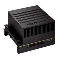
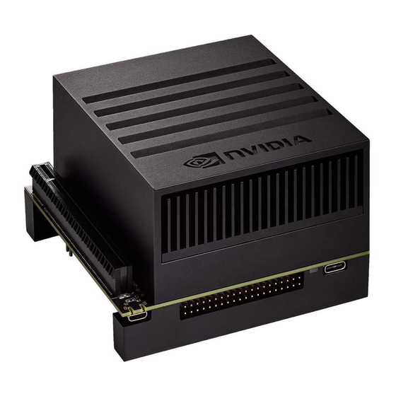
Nvidia Jetson AGX Xavier Series Design Manual (157 pages)
Brand:
Nvidia
| Category:
Computer Hardware
| Size: 4 MB
Table of Contents
Table of Contents
7
Chapter 1. Introduction
16
References
16
Abbreviations and Definitions
16
Table 1-1. Abbreviations and Definitions
17
Chapter 2. Jetson AGX Xavier
18
Table 2-1. Jetson AGX Xavier Specifications
18
Figure 2-1. System Block Diagram
19
Table 2-2. Connector Pinout Matrix Part 1: Columns A-F
20
Table 2-3. Connector Pinout Matrix Part 2: Columns G-L
21
Chapter 3. Main Connector Details
23
Figure 3-1. 699-Pin Connector Dimensions
23
Connector Pin Orientations
24
Figure 3-2. 699-Pin Connector Pin Orientations
24
Module to Carrier Board Spacing Details
25
Figure 3-3. 5.5 MM Height on Carrier Board - Molex Part # 2034560003
25
Figure 3-4. 2.5 MM Height on Carrier Board - Molex Part # 2048430001
25
Module to Carrier Board Standoff Height Recommendations
26
Table 3-1. Standoff Height Calculations for 5.5 MM Height Connector Case
26
Module Installation and Removal
27
Table 3-2. Standoff Height Calculations for 2.5 MM Height Connector Case
27
Figure 3-5. Module Removal
28
Chapter 4. Reference Design Considerations
29
Chapter 5. Power
31
Table 5-1. Power, System, and Thermal Pin Descriptions
31
Supply Allocation
33
Figure 5-1. Power Block Diagram
33
Table 5-2. Internal Power Subsystem Allocation
33
Power Sequencing
34
Figure 5-2. Power up Sequence - Power Button Case
35
Figure 5-3. Power down Sequence Controlled Case
36
Figure 5-4. Power down Sequence Uncontrolled Case
36
SYS_VIN_HV Input
37
Power-On
37
Power-On no MCU
37
Figure 5-5. Simplified DC Jack Power Connections
37
Auto Power-On Option no MCU
38
Figure 5-6. Simplified Button Power-On Circuitry
38
Table 5-3. Simplified Button Power Circuitry Timing
38
Power Button Supervisor MCU Power-On
39
Figure 5-7. Optional ACOK Circuitry
39
Table 5-4. Power Button Supervisor Control Signals
39
Defined Behaviors
40
Power off -> Power on (Power Button Case)
40
Figure 5-8. Power-On Button Circuit
40
Power off -> Power on (Auto-Power-On Case)
41
Figure 5-9. Power-OFF to on Sequence Power Button Case
41
Table 5-5. Power-OFF to on Timing Power Button Case
41
Power on -> Power off (Power Button Held Low > 10 Seconds)
42
Figure 5-10. Power-OFF to on Sequence Auto Power-On Case
42
Table 5-6. Power-OFF to on Timing Auto Power-On Case
42
Power Discharge
43
DV/Dt Circuit Considerations
43
Figure 5-11. Power-On to off Power Button Held Low > 10 Seconds
43
Table 5-7. Power-On to off Timing Power Button Held Low > 10 Seconds
43
Power and Voltage Monitoring
45
Power Loss Detection
45
Figure 5-12. Power Discharge
45
Power Monitor
46
Figure 5-13. VIN Loss Detection Circuit
46
Figure 5-14. Power Monitor
46
Deep Sleep or SC7
47
Table 5-8. Jetson AGX Xavier Signal Wake Events
47
Chapter 6. General Routing Guidelines
49
Signal Name Conventions
49
Table 6-1. Signal Type Codes
49
Routing Guideline Format
50
Signal Routing Conventions
50
Routing Guidelines
50
General PCB Routing Guidelines
51
Figure 6-1. Signal Routing Example
51
Chapter 7. USB, Pcie, and UFS
52
Table 7-1. USB 2.0 Pin Descriptions
52
Table 7-2. UPHY Data Lane Pin Descriptions USB 3.1, Pcie, and UFS
52
Table 7-3. NVHS for Pcie X8 Data Lan Pin Descriptions
53
Table 7-4. Pcie Clock and Control Pin Descriptions
54
Table 7-5. UFS and Miscellaneous USB Control Pin Descriptions
55
Table 7-6. USB 3.1, Pcie and UFS Lane Mapping Configurations
55
Usb
56
Figure 7-1. Simple USB Type a Connection Example
56
Figure 7-2. Jetson AGX Xavier Carrier Board Design USB Type C Connection Example
57
Figure 7-3. USB 3.1 USB Micro AB Connection Example
57
USB 2.0 Design Guidelines
58
USB 3.1 Design Guidelines
58
Table 7-7. USB 2.0 Interface Signal Routing Requirements
58
Table 7-8. USB 3.1 Interface Signal Routing Requirements
58
Common USB Routing Guidelines
61
PCI Express
62
Table 7-9. USB 2.0 Signal Connections
62
Table 7-10. USB 3.1 Signal Connections
62
Table 7-11. Recommended USB Observation Test Points for Initial Boards
62
Figure 7-4. Pcie Root Port Connection Example
63
Figure 7-5. Pcie Endpoint Connection Example
64
Pcie Design Guidelines up to Gen3
65
Table 7-12. Pcie Interface Signal Routing Requirements up to Gen3
65
Figure 7-6. Insertion Loss S-Parameter Plot (SDD21)
67
Pcie Gen4 Design Guidelines
68
Table 7-13. Pcie Gen4 Interface Signal Routing Requirements
68
Table 7-14. Pcie Signal Connections Module I/Fs Configured as Root Ports
69
Table 7-15. Pcie Signal Connections Module I/F Configured as Endpoint
71
Table 7-16. Recommended Pcie Observation Test Points for Initial Boards
71
Ufs
72
UFS Design Guidelines
72
Figure 7-7. UFS Connections Example
72
Table 7-17. UFS Interface Signal Routing Requirements
72
Table 7-18. UFS Signal Connections
73
Chapter 8. Gigabit Ethernet
74
Table 8-1. Jetson AGX Xavier Gigabit Ethernet Pin Descriptions
74
Figure 8-1. Ethernet Connections
75
Figure 8-2. Gigabit Ethernet Magnetics and RJ45 Connections
75
Table 8-2. RGMII Interface Signal Routing Requirements
76
Table 8-3. Ethernet MDI Interface Signal Routing Requirements
76
Table 8-4. Ethernet Signal Connections
77
Table 8-5. Recommended Gigabit Ethernet Observation Test Points for Initial Boards
77
Chapter 9. Display
78
Table 9-1. Jetson AGX Xavier HDMI, Edp, and DP Pin Description
78
Table 9-2. DP and HDMI Pin Mapping
79
DP and Edp
80
Figure 9-1. DP and Edp Connection Example
80
DP and Edp Routing Guidelines
81
Figure 9-2. DP and Edp Differential Main Link Topology
81
Table 9-3. DP and Edp Main Link Signal Routing Requirements
81
Hdmi
84
Table 9-4. DP and Edp Signal Connections
84
Table 9-5. Recommended DP and Edp Observation Test Points for Initial Boards
84
Figure 9-3. HDMI Connection Example
85
Figure 9-4. HDMI CLK and Data Topology
86
Table 9-6. HDMI Interface Signal Routing Requirements
86
Table 9-7. HDMI Signal Connections
91
Table 9-8. Recommended HDMI and DP Observation Test Points for Initial Boards
91
Chapter 10. Video Input
92
Mipi Csi
92
Table 10-1. Jetson AGX Xavier CSI Pin Description
92
Table 10-2. Jetson AGX Xavier Camera Miscellaneous Pin Description
95
Table 10-3. CSI Configurations D-PHY Mode
95
Table 10-4. CSI Configurations C-PHY Mode - X2 and X4
97
Table 10-5. CSI Configurations C-PHY - X3 and X1
98
Figure 10-1. Camera Control Connections
99
Figure 10-2. Camera CSI D-PHY Connections
100
Figure 10-3. Camera CSI C-PHY Connections
101
CSI D-PHY Design Guidelines
102
Table 10-6. MIPI CSI D-PHY Interface Signal Routing Requirements
102
CSI C-PHY Mode Design Guidelines
103
Table 10-7. MIPI CSI C-PHY Interface Signal Routing Requirements
103
Table 10-8. MIPI CSI Signal Connections
103
SLVS Camera Interface
104
Table 10-9. Miscellaneous MIPI Camera Connections
104
Table 10-10. Recommended CSI Observation Test Points for Initial Boards
104
Table 10-11. Jetson AGX Xavier SLVS EC Camera Pin Description
104
Figure 10-4. SLVS Connections
106
SLVS Design Guidelines
107
Table 10-12. SLVS Interface Signal Routing Requirements
107
Table 10-13. SLVS Camera Signal Connections
108
Table 10-14. Non-Module SLVS Reference Clock Connections
108
Chapter 11. SDIO and SD Card
109
SD Card
109
Table 11-1. SDIO, SD Card, and Emmc Interface Mapping
109
Table 11-2. Jetson AGX Xavier SDMMC Pin Descriptions
109
Figure 11-1. Micro SD Card Socket Connection Example
110
Table 11-3. SDCARD Interface Signal Routing Requirements
110
Table 11-4. SD Card Loading Vs. Drive Type
111
Table 11-5. SDCARD Signal Connections
112
Table 11-6. Recommended SDCARD Observation Test Points for Initial Boards
112
Chapter 12. Audio
113
Table 12-1. Jetson AGX Xavier Audio Pin Description
113
Table 12-2. I2S Interface Mapping
114
Figure 12-1. Audio Device Connections
115
I2S Design Guidelines
116
Table 12-3. I2S Interface Signal Routing Requirements
116
Table 12-4. I2S and Miscellaneous Codec Signal Connections
116
DMIC Design Guidelines
117
Table 12-5. DMIC Interface Signal Routing Requirements
117
Table 12-6. DMIC Signal Connections
117
Chapter 13. Miscellaneous Interfaces
118
I2C
118
Table 13-1. Jetson AGX Xavier I2C Pin Description
118
Table 13-2. I2C Interface Mapping
119
I2C Design Guidelines
120
Figure 13-1. I2C Connections
120
Table 13-3. I2C Interface Signal Routing Requirements
121
Table 13-4. I2C Signal Connections
121
Bounce
122
Spi
122
Table 13-5. De-Bounce Settings - Fast Mode Plus, Fast Mode, and Standard Mode
122
Table 13-6. Jetson AGX Xavier SPI Pin Description
122
SPI Design Guidelines
123
Figure 13-2. SPI Connections
123
Figure 13-3. Basic SPI Master and Slave Connections
123
Figure 13-4. SPI Point-Point Topology
123
Figure 13-5. SPI Star Topologies
123
Figure 13-6. SPI Daisy Topologies
124
Table 13-7. SPI Interface Signal Routing Requirements
124
Table 13-8. SPI Signal Connections
124
Table 13-9. Recommended SPI Observation Test Points for Initial Boards
124
Uart
125
Table 13-10. Jetson AGX Xavier UART Pin Description
125
Figure 13-7. Jetson AGX Xavier UART Connections
126
Table 13-11. UART Signal Connections
126
Can
127
Figure 13-8. Jetson AGX Xavier CAN Connections
127
Table 13-12. Reserved UART4_RX Routing Requirements
127
Table 13-13. Jetson AGX Xavier CAN Pin Description
127
Table 13-14. CAN Interface Signal Routing Requirements
128
Table 13-15. CAN Signal Connections
128
Chapter 14. Fan
129
Table 14-1. Jetson AGX Xavier Fan Pin Description
129
Figure 14-1. Jetson AGX Xavier Fan Connection Example
130
Table 14-2. Fan Signal Connections
130
Chapter 15. Debug and Strapping
131
USB Recovery Mode
131
JTAG and Debug UART
132
Figure 15-1. JTAG and UART Debug Connections
132
Figure 15-2. Simple Debug UART Header Connections
132
Jtag
133
Table 15-1. Jetson AGX Xavier JTAG Pin Description
133
Table 15-2. JTAG Signal Connections
133
Debug UART
134
Strapping Pins
134
Table 15-3. Debug UART Connections
134
Table 15-4. Strapping Pins
134
Boundary Scan Test Mode
135
Figure 15-3. Example Buffer between Pin Associated with Soc Strap and Connected Device
135
Figure 15-4. Boundary Scan Connections
135
Safety MCU Jaxi Only
136
Table 15-5. Safety MCU Related Partial Pin Descriptions
136
Figure 15-5. Safety MCU Connections
137
Chapter 16. Pads
138
MPIO Pad Behavior When Associated Power Rail Is Enabled
138
Schmitt Trigger Usage
138
Pins Pulled and Driven During Power-On
138
Pad Drive Strength
139
Table 16-1. MPIO Maximum Output Drive Current
139
Chapter 17. Unused Interface Terminations
140
Unused MPIO Interfaces
140
Unused SFIO Interface Pins
140
Table 17-1. Unused MPIO Pins and Pin Groups
140
Chapter 18. Design and Bring-Up Checklists
141
Chapter 19. General Layout Guidelines
142
Via Guidelines
142
Via Count and Trace Width
142
Via Placement
142
Via Placement and Power and Ground Corridors
142
Figure 19-1. Via Placement for Good Power Distribution
143
Figure 19-2. Good Current Flow Resulting from Correct Via Placement
143
Figure 19-3. Poor Current Flow Resulting from Incorrect Via Placement
143
Connecting Vias
144
Trace Guidelines
144
Layer Stack-Up
144
Trace Length
144
Chapter 20. Stack-Ups
145
Reference Design Stack-Ups
145
Importance of Stack-Up Definition
145
Impact of Stack-Up Definition on Design
145
Chapter 21. Transmission Line Primer
146
Basic Board Level Transmission Line Theory
146
Characteristics
146
Figure 21-1. Typical Transmission Lin Circuit
146
Physical Transmission Line Types
147
Microstrip Transmission Line
147
Stripline Transmission Line
147
Figure 21-2. Microstrip Transmission Line
147
Figure 21-3. Stripline Transmission Line
147
Drive Characteristics
148
Receiver Characteristics
148
Transmission Lines and Reference Planes
149
Figure 21-4. Transmission Line Height
149
Figure 21-5. Crosstalk on Reference Plane
150
Figure 21-6. Power Plane Cuts Example
150
Figure 21-7. Power Plane Cuts Example When Decouple Capacitors Are Abundant
150
Figure 21-8. Switching Reference Planes
151
Figure 21-9. Reference Plane Switch Using Via
151
Chapter 22. Design Guideline Glossary
152
Advertisement
Advertisement
Related Products
Nvidia Jetson Orin NX
Nvidia JETSON DEVELOPER KIT
Nvidia Jetson AGX Orin Series
Nvidia JETSON AGX XAVIER
Nvidia JETSON NANO
Nvidia JETSON XAVIER NX
Nvidia Jetson Nano Developer Kit
Nvidia Jetson Orin NX Series
Nvidia Jetson Orin Nano Series
Nvidia 6200
Nvidia Categories
Video Card
Computer Hardware
Motherboard
Switch
Adapter
More Nvidia Manuals
Login
Sign In
OR
Sign in with Facebook
Sign in with Google
Upload manual
Upload from disk
Upload from URL