Table of Contents
Advertisement
Quick Links
Advertisement
Table of Contents

Related Manuals for EUROCOM B7110


Summary of Contents for EUROCOM B7110
- Page 3 Preface Notebook Computer B7110 Service Manual...
- Page 4 Preface Notice The company reserves the right to revise this publication or to change its contents without notice. Information contained herein is for reference only and does not constitute a commitment on the part of the manufacturer or any subsequent ven- dor.
- Page 5 Preface About this Manual This manual is intended for service personnel who have completed sufficient training to undertake the maintenance and inspection of personal computers. It is organized to allow you to look up basic information for servicing and/or upgrading components of the B7110 series notebook PC.
- Page 6 Preface IMPORTANT SAFETY INSTRUCTIONS Follow basic safety precautions, including those listed below, to reduce the risk of fire, electric shock and injury to per- sons when using any electrical equipment: 1. Do not use this product near water, for example near a bath tub, wash bowl, kitchen sink or laundry tub, in a wet basement or near a swimming pool.
-
Page 7: Instructions For Care And Operation
Preface Instructions for Care and Operation The notebook computer is quite rugged, but it can be damaged. To prevent this, follow these suggestions: Don’t drop it, or expose it to shock. If the computer falls, the case and the components could be damaged. Do not expose the computer Do not place it on an unstable Do not place anything heavy... -
Page 8: Power Safety
Preface Avoid interference. Keep the computer away from high capacity transformers, electric motors, and other strong mag- netic fields. These can hinder proper performance and damage your data. Take care when using peripheral devices. Use only approved brands of Unplug the power cord before peripherals. -
Page 9: Battery Precautions
Preface Battery Precautions • Only use batteries designed for this computer. The wrong battery type may explode, leak or damage the computer. • Do not continue to use a battery that has been dropped, or that appears damaged (e.g. bent or twisted) in any way. Even if the computer continues to work with a damaged battery in place, it may cause circuit damage, which may possibly result in fire. -
Page 10: Figure 1
Preface Related Documents You may also need to consult the following manual for additional information: User’s Manual on CD/DVD This describes the notebook PC’s features and the procedures for operating the computer and its ROM-based setup pro- gram. It also describes the installation and operation of the utility programs provided with the notebook PC. System Startup 1. -
Page 11: Table Of Contents
Preface Contents Introduction ..........1-1 LCD ....................A-5 HDD ....................A-6 Overview ..................1-1 SATA DVD Super-Multi ............... A-7 Specifications ..................1-2 SATA Blu-Ray Combo ..............A-8 External Locator - Top View with LCD Panel Open ......1-4 Schematic Diagrams......... B-1 External Locator - Front & Right Side Views .........1-5 External Locator - Left Side &... - Page 12 Preface IBEXPEAK - M 8/9 ..............B-27 Unzip the downloaded files to a bootable CD/DVD/ or USB Flash IBEXPEAK - M 9/9 ..............B-28 drive ....................C-1 New Card, Mini PCIE ..............B-29 Set the computer to boot from the external drive ......C-1 3G, CCD, TPM ................
-
Page 13: Introduction
Introduction Chapter 1: Introduction Overview This manual covers the information you need to service or upgrade the B7110 series notebook computer. Information about operating the computer (e.g. getting started, and the Setup utility) is in the User’s Manual. Information about dri- vers (e.g. -
Page 14: Specifications
Introduction Specifications Processor Options Video Adapter Intel® Core™ i7 Processor Intel® GMA HD and NVIDIA® GeForce GT330M i7-620M (2.66GHz) Supports NVIDIA® Optimus Technology 4MB L3 Cache & 1066MHz FSB Intel Integrated GPU (Intel® GMA HD): Intel® Core™ i5 Processor Latest Specification Information Shared Memory Architecture (DVMT) up to 1.7GB i5-540M (2.53GHz), i5-520M (2.4GHz),... - Page 15 Introduction Keyboard Environmental Spec Full-size “WinKey” keyboard (with numeric keypad) Temperature ° ° Operating: 5 C - 35 Non-Operating: -20°C - 60°C Pointing Device Relative Humidity Built-in Touchpad (scrolling key functionality integrated) Operating: 20% - 80% Non-Operating: 10% - 90% Interface Communication Three USB 2.0 Ports and One USB 3.0 Port...
-
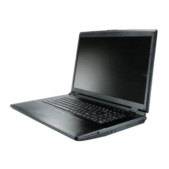
Page 16: External Locator - Top View With Lcd Panel Open
Introduction External Locator - Top View with LCD Panel Open Figure 1 Top View 1. Built-In PC Ca- mera (optional) 2. LCD 3. Power Button 4. GPU Button 5. LED Indicators 6. Hot Key Buttons 7. Keyboard 8. Built-In Microphone 9. -
Page 17: External Locator - Front & Right Side Views
Introduction External Locator - Front & Right Side Views Figure 2 Front View 1. LED Indicators FRONT VIEW Figure 3 Right Side View 1. Headphone-Out RIGHT SIDE VIEW Jack 2. Microphone-In Jack 3. S/PDIF-Out Jack 4. USB 2.0 Port 5. Optical Device Drive Bay 6. -
Page 18: External Locator - Left Side & Rear View
Introduction External Locator - Left Side & Rear View Figure 4 Left Side View 1. External Monitor Port 2. RJ-45 LAN Jack LEFT SIDE VIEW 3. HDMI-Out Port 4. 2 * USB 2.0 Ports 5. Vent 6. eSATA Port 7. USB 3.0 Port or USB 2.0 Port (Note: It depends on your purchase... -
Page 19: External Locator - Bottom View
Introduction External Locator - Bottom View Figure 6 Bottom View 1. Battery 2. Component Bay Cover 3. Vents 4. Hard Disk Bay Cover 5. Speakers Overheating To prevent your com- puter from overhea- ting, make sure no- thing blocks any vent while the computer is in use. -
Page 20: Mainboard Overview - Top (Key Parts)
Introduction Mainboard Overview - Top (Key Parts) Figure 7 Mainboard Top Key Parts 1. JMC251 2. KBC-ITE IT8502E 3. Clock Generator 4. Azalia Codec 1 - 8 Mainboard Overview - Top (Key Parts) -
Page 21: Mainboard Overview - Bottom (Key Parts)
Introduction Mainboard Overview - Bottom (Key Parts) Figure 8 Mainboard Bottom Key Parts 1. CPU Socket (no CPU installed) 2. Memory Slots DDR3 SO-DIMM 3. Mini-Card Connector (WLAN Module) 4. Platform Controller 5. 3-in-1 Card Reader 6. VGA Mainboard Overview - Bottom (Key Parts) 1 - 9... -
Page 22: Mainboard Overview - Top (Connectors)
Introduction Mainboard Overview - Top (Connectors) Figure 9 Mainboard Top Connectors 1. External Monitor Port 2. RJ-45 LAN Jack 3. HDMI-Out Port 4. USB Ports 5. eSATA Port 6. Microphone Cable Connector 7. Audio Board Connector 8. Fingerprint and TouchPad Cable Connector 9. -
Page 23: Mainboard Overview - Bottom (Connectors)
Introduction Mainboard Overview - Bottom (Connectors) Figure 10 Mainboard Bottom Connectors 1. Bluetooth Cable Connector 2. HDD & ODD Connector 3. CMOS Battery Connector 4. Speaker Cable Connector 5. CPU Fan Cable Connector 6. LCD Cable Connector 7. CCD Cable Connector 8. - Page 24 Introduction 1 - 12...
-
Page 25: Disassembly
Disassembly Chapter 2: Disassembly Overview This chapter provides step-by-step instructions for disassembling the B7110 series notebook’s parts and subsystems. When it comes to reassembly, reverse the procedures (unless otherwise indicated). We suggest you completely review any procedure before you take the computer apart. Procedures such as upgrading/replacing the RAM, optical device and hard disk are included in the User’s Manual but are repeated here for your convenience. -
Page 26: Maintenance Tools
Disassembly NOTE: All disassembly procedures assume that the system is turned OFF, and disconnected from any power supply (the battery is removed too). Maintenance Tools The following tools are recommended when working on the notebook PC: • M3 Philips-head screwdriver •... -
Page 27: Maintenance Precautions
Disassembly Maintenance Precautions The following precautions are a reminder. To avoid personal injury or damage to the computer while performing a re- moval and/or replacement job, take the following precautions: Power Safety Warning 1. Don't drop it. Perform your repairs and/or upgrades on a stable surface. If the computer falls, the case and other Before you undertake components could be damaged. -
Page 28: Disassembly Steps
Disassembly Disassembly Steps The following table lists the disassembly steps, and on which page to find the related information. PLEASE PERFORM THE DISASSEMBLY STEPS IN THE ORDER INDICATED. To remove the Battery: To remove the Bluetooth Module: 1. Remove the battery page 2 - 5 1. -
Page 29: Removing The Battery
Disassembly Removing the Battery Figure 1 Battery Removal 1. Turn the computer off, and turn it over. 2. Slide the latch in the direction of the arrow (Figure 1a a. Slide the latch and hold in 3. Slide the latch in the direction of the arrow, and hold it in place (Figure 1a place. -
Page 30: Removing The Hard Disk Drive
Disassembly Removing the Hard Disk Drive The hard disk drive can be taken out to accommodate other 2.5" serial (SATA) hard disk drives with a height of 9.5mm Figure 2 (h). Follow your operating system’s installation instructions, and install all necessary drivers and utilities (as outlined in HDD Assembly Chapter 4 of the User’s Manual) when setting up a new hard disk. - Page 31 Disassembly 3. Remove the hard disk bay cover (Figure 3b Figure 3 4. Grip the mylar cover and slide the hard disk in the direction of arrow (Figure 3c HDD Assembly 5. Lift the hard disk out of the bay (Figure 3d Removal (cont’d.) 6.
-
Page 32: Removing The System Memory (Ram)
Disassembly Removing the System Memory (RAM) Figure 4 RAM Module The computer has two memory sockets for 204 pin Small Outline Dual In-line Memory Modules (SO-DIMM) supporting Removal DDR3 1066MHz. The main memory can be expanded up to 8GB. The SO-DIMM modules supported are 1024MB, and 2048MB and DDRIII Modules. - Page 33 Disassembly 5. Gently pull the two release latches ( on the sides of the memory socket in the direction indicated by the Figure 5 arrows (Figure 5c). RAM Module Removal (cont’d.) c. Pull the release latches. d. Remove the module(s). ...
-
Page 34: Removing The Optical (Cd/Dvd) Device
Disassembly Removing the Optical (CD/DVD) Device Figure 6 Optical Device 1. Turn off the computer, remove the battery (page 2 - 5) and hard disk (page 2 - Removal 2. Remove the screw at point (Figure 6a , and use a screwdriver to carefully push out the optical device point (Figure 6b a. -
Page 35: Removing And Installing The Processor
Disassembly Removing and Installing the Processor Figure 7 Processor Removal Processor Removal Procedure 1. Turn off the computer, remove the battery (page 2 - 5) and the component bay cover (page 2 - a. Remove the cover and 2. The CPU heat sink will be visible at point (Figure 7a) on the mainboard. - Page 36 Disassembly 5. Turn the release latch towards the unlock symbol , to release the CPU (Figure 8d). Figure 8 6. Carefully (it may be hot) lift the CPU up out of the socket (Figure 8e). Processor Removal 7. See page 2 - 13 for information on inserting a new CPU.
- Page 37 Disassembly Processor Installation Procedure Figure 9 1. Insert the CPU (Figure 9a , pay careful attention to the pin alignment, it will fit only one way (DO NOT FORCE Processor Installation IT!), and turn the release latch towards the lock symbol (Figure 9b).
-
Page 38: Removing The Wireless Lan Module
Disassembly Removing the Wireless LAN Module Figure 10 Wireless LAN 1. Turn off the computer, remove the battery (page 2 - 5) and the component bay cover (page 2 - Module Removal 2. The Wireless LAN module will be visible at point (Figure 10a on the mainboard. -
Page 39: Removing The Bluetooth Module
Disassembly Removing the Bluetooth Module Figure 11 Bluetooth Module 1. Turn off the computer, remove the battery (page 2 - 5) and the component bay cover (page 2 - Removal 1. Locate the Bluetooth module at point Figure 11a 2. Remove screw and carefully disconnect the Bluetooth module from the connector and the cable Figure... -
Page 40: Removing The Keyboard
Disassembly Removing the Keyboard Figure 12 Keyboard Removal 1. Turn off the computer and remove the battery (page 2 - 2. Remove screws & and use a screwdriver to carefully push out the top cover module at point (Figure a. Remove screws and use a 12a). -
Page 41: Part Lists
Part Lists Appendix A:Part Lists This appendix breaks down the B7110 series notebook’s construction into a series of illustrations. The component part numbers are indicated in the tables opposite the drawings. Note: This section indicates the manufacturer’s part numbers. Your organization may use a different system, so be sure to cross-check any relevant documentation. -
Page 42: Part List Illustration Location
Part Lists Part List Illustration Location The following table indicates where to find the appropriate part list illustration. Table A - 1 Part List Illustration Part B7110 Location page A - 3 page A - 4 Bottom page A - 5 page A - 6 SATA DVD Super-Multi page A - 7... -
Page 43: Top
Part Lists Figure A - 1 非耐落 黑色 灰色 Top A - 3... -
Page 44: Bottom
Part Lists Bottom Figure A - 2 Bottom A - 4 Bottom... -
Page 45: Lcd
Part Lists Figure A - 3 非耐落 LCD A - 5... -
Page 46: Hdd
Part Lists Figure A - 4 A - 6 HDD... -
Page 47: Sata Dvd Super-Multi
Part Lists SATA DVD Super-Multi Figure A - 5 SATA DVD Super- Multi SATA DVD Super-Multi A - 7... -
Page 48: Sata Blu-Ray Combo
Part Lists SATA Blu-Ray Combo Figure A - 6 SATA Blu-Ray Combo A - 8 SATA Blu-Ray Combo... -
Page 49: Schematic Diagrams
Schematic Diagrams Appendix B: Schematic Diagrams This appendix has circuit diagrams of the B7110 notebook’s PCB’s. The following table indicates where to find the ap- propriate schematic diagram. Table B - 1 SCHEMATIC Diagram - Page Diagram - Page Diagram - Page DIAGRAMS System Block Diagram - Page B - 2 IBEXPEAK- M 1/9 - Page B - 20... -
Page 50: Schematic Diagrams
Schematic Diagrams System Block Diagram B4100M & B5100M System Block Diagram VDD3,VDD5 B4100 POWER SWITCH BOARD 14.318 MHz GPU NVDIDA N11x NVVDD FINGER PRINTER BOARD Clock Generator PCIE*8 SLG8SP585 5V,3V,5VS,3VS,1.5VS, Arrandale 1.8VS,+1.5S_CPU AUDIO BOARD PHONE JACK x3, USB x1 800/1067/1333 MHz Nvidia PROCESSOR RJ-11... -
Page 51: Clock Generator
Schematic Diagrams Clock Generator CLKGEN POWER CLOCK GENERATOR C LK_VC C1 CLK_VCC 2 C LK_VC C1 3. 3VS *HCB1608KF-121T25_32mil_short VDD _DOT VDD _SRC _I/O VDD _27 VDD _CPU _I/O C482 C475 C 483 VDD _SRC VDD _CPU 0.1u_16V_Y 5V_04 1u_16V_X5R_06 C LK_BUF_DOT96_P 20 VDD _REF DOT_96... -
Page 52: Cpu 1/7 (Dmi, Peg, Fdi
Schematic Diagrams CPU 1/7 (DMI, PEG, FDI) PROCESSOR ( DMI,PEG,FDI ) U40A 20 mil PEG_IRCOMP_R R427 49.9_1%_04 PEG_ICOMPI PEG_ICOMPO DMI_TXN0 DMI_RX#[0] PEG_RCOMPO EXP_RBIAS R429 750_1%_04 DMI_TXN1 DMI_RX#[1] PEG_RBIAS DMI_TXN2 DMI_RX#[2] H8_0D4_4 H8_0D4_4 H8_0D4_4 PEG_RX#0 13 DMI_TXN3 DMI_RX#[3] PEG_RX#[0] PEG_RX#1 13 PEG_RX#[1] PEG_RX#2 13 DMI_TXP0... -
Page 53: Cpu 2/7 (Clk, Misc, Jtag
Schematic Diagrams CPU 2/7 (CLK, MISC, JTAG) Processor Compensation PROCESSOR 2/7 ( CLK,MISC,JTAG ) Signals H_COMP0 R419 49.9_1%_04 U40B DDR3 Compensation Signals H_COMP1 H_COMP3 AT23 R433 49.9_1%_04 COMP3 BCLK_CPU_P 24 BCLK TRACE WIDTH 10MIL, LENGTH <500MILS H_COMP2 AT24 SM_RCOMP_0 R441 100_1%_04 BCLK_CPU_N 24 COMP2... -
Page 54: Cpu 3/7 (Ddr3
Schematic Diagrams CPU 3/7 (DDR3) PROCESSOR ( DDR3 ) U40C U40D M_A_DQ[63:0] M_CLK_DDR0 10 M_B_DQ[63:0] SA_CK[0] M_CLK_DDR#0 10 M_C LK_DD R2 11 SA_C K#[0] SB_C K[0] M_CKE0 10 M_C LK_DD R#2 11 SA_CKE[0] SB_CK#[0] M_A_DQ0 M_B_DQ0 M_C KE2 11 SA_D Q[0] SB_DQ[0] SB_C KE[0] M_A_DQ1... -
Page 55: Cpu 4/7 (Power
Schematic Diagrams CPU 4/7 (Power) PROCESSOR ( POWER ) U40F PROCESSOR CORE POWER PROCESSOR UNCORE POWER VCORE 1.1VS_VTT VTT TOTAL 21A AG35 AH14 VCC1 VTT0_1 AG34 AH12 ICCMAX Maximum Processor SV 52 VCC2 VTT0_2 AG33 AH11 C177 C186 C170 C190 C204 C175 C585... -
Page 56: Cpu 5/7 (Graphics Power
Schematic Diagrams CPU 5/7 (Graphics Power) PROCESSOR ( GRAPHICS POWER ) VGFX_CORE U40G AT21 VAXG1 AT19 AR22 GPUVCCSENSE 42 VAXG2 VAXG_SENSE AT18 AT22 C153 C152 R120 VAXG3 VSSAXG_SENSE GPUVSSSENSE 42 AT16 *0_04 VAXG4 AR21 10u_6.3V_X5R_06 10u_6.3V_X5R_06 VAXG5 AR19 VAXG6 AR18 VAXG7 AR16 AM22... -
Page 57: Cpu 6/7 (Gnd
Schematic Diagrams CPU 6/7 (GND) PROCESSOR ( GND ) U40H U40I AT20 AE34 VSS1 VSS81 AT17 AE33 VSS2 VSS82 AR31 AE32 VSS3 VSS83 VSS161 AR28 AE31 VSS4 VSS84 VSS162 AR26 AE30 VSS5 VSS85 VSS163 AR24 AE29 VSS6 VSS86 VSS164 AR23 AE28 VSS7 VSS87... -
Page 58: Cpu 7/7 (Reserved
Schematic Diagrams CPU 7/7 (RESERVED) PROCESSOR 7/7 ( RESERVED ) U40E AJ13 RSVD32 AJ12 R238 0_04 RSVD33 AP25 RSVD1 AL25 AH25 PCI-Express Configuration Select RSVD2 RSVD34 AL24 AK26 VREF_CH_A_DIMM MVREF_DQ_DIM0 RSVD3 RSVD35 AL22 RSVD4 AJ33 AL26 1 : Single PEG CFG0 RSVD5 RSVD36... -
Page 59: Ddr3 So-Dimm_0
Schematic Diagrams DDR3 SO-DIMM_0 SO-DIMM A CHANGE TO STANDARD C310 *10p_50V_NPO_04 M_CLK_DDR0 M_CLK_DDR#0 JDIMM1A M_A_A[15:0] M_A_DQ[63:0] 5 M_A_A0 M_A_DQ0 C298 *10p_50V_NPO_04 JDIMM1B M_CLK_DDR1 M_CLK_DDR#1 M_A_A1 M_A_DQ1 M_A_A2 M_A_DQ2 M_A_A3 M_A_DQ3 1.5V M_A_A4 M_A_DQ4 M_A_A5 M_A_DQ5 VDD1 VSS16 M_A_A6 M_A_DQ6 VDD2 VSS17 M_A_A7 M_A_DQ7... -
Page 60: Ddr3 So-Dimm_1
Schematic Diagrams DDR3 SO-DIMM_1 SO-DIMM B CHANGE TO STANDARD C361 *10p_50V_NPO_04 JDIMM2A M_B_A[15:0] M_B_DQ[63:0] 5 M_CLK_DDR2 M_CLK_DDR#2 M_B_A0 M_B_DQ0 JDIMM2B M_B_A1 M_B_DQ1 M_B_A2 M_B_DQ2 C355 *10p_50V_NPO_04 1.5V M_CLK_DDR3 M_CLK_DDR#3 M_B_A3 M_B_DQ3 M_B_A4 M_B_DQ4 M_B_A5 M_B_DQ5 VDD1 VSS16 M_B_A6 M_B_DQ6 VDD2 VSS17 M_B_A7 M_B_DQ7... -
Page 61: Panel, Inverter, Crt
Schematic Diagrams Panel, Inverter, CRT PANEL 3.3VS *WC M3216F2S-161T03 *WC M3216F2S-161T03 3. 3VS RLVDS-L2N LVDS-L2N RLVDS-U2N LVD S-U2N LVD S-L2N 22 LVDS-U 2N 22 R353 R358 NEAR PIN4,5 U 32 BRIGHTNESS RLVDS-L2P LVDS-L2P RLVDS-U2P LVD S-U2P LVD S-L2P 22 LVDS-U 2P 22 VOUT J_LCD1 2.2K_04... -
Page 62: Vga Pci-E Interface
Schematic Diagrams VGA PCI-E Interface H8_0D4_4 H8_0D4_4 H8_0D4_4 U36A PEX_VDD 1/16 PCI_EXPRESS AK16 PEX_IOVDD AK17 PEX_IOVDD 3V3_RUN BIOS ROM AK21 C103 C101 C109 PEX_IOVDD AK24 PEX_IOVDD AK27 0.1u_16V_Y5V_04 0.1u_16V_Y5V_04 1u_6.3V_X5R_04 10u_6.3V_X5R_06 10u_6.3V_X5R_06 3V3_RUN PEX_IOVDD 3V3_RUN 0.1u_16V_Y5V_04 1u_6.3V_X5R_04 4.7u_6.3V_X5R_06 R375 3V3_RUN PLACE NEAR BALLS PLACE NEAR BGA U36K... -
Page 63: Vga Frame Buffer Interface
Schematic Diagrams VGA Frame Buffer Interface Frame Buffer Interface U36C U36B 2/16 FBA 3/16 FBC FBVDDQ FBVDDQ FBC_D[63:0] GT216 FBC_D[63:0] FBA_D[63:0] GT216 FBA_D[63:0] FBC_D0 FBC_D0 FBC _D 26 FBVDDQ FBA_D0 FBC_D1 FBA_D0 FBA_D14 FBVDDQ FBC_D1 FBC _D 24 FBVDDQ FBA_D1 FBC_D2 FBA_D1 FBA_D15... -
Page 64: Vga Frame Buffer A
Schematic Diagrams VGA Frame Buffer A FBVDDQ Frame Buffer Partition A FBA_CMD[30:0] FBA_CMD [30:0] C589 C191 C182 C172 FBA_D[63:0] FBA_D[63:0] FBADQM[7:0] 1u_6.3V_X5R_04 1u_6.3V_X5R_04 1u_6.3V_X5R_04 1u_6.3V_X5R_04 FBAD QM[7:0] FBADQS_W P[7:0] FBAD QS_WP[7:0] FBADQS_RN [7:0] FBADQS_RN [7:0] FBVD DQ FBVD DQ FBVD DQ FBVD DQ C 571 C 201... -
Page 65: Vga Frame Buffer C
Schematic Diagrams VGA Frame Buffer C FBC_CMD[30:0] FBC_CMD[30:0] Frame Buffer Partition C FBC_D[63:0] FBC_D[63:0] FBCDQM[7:0] FBCDQM[7:0] FBCDQS_WP[7:0] FBCDQS_WP[7:0] FBCDQS_RN[7:0] FBCDQS_RN[7:0] FBVDDQ FBVDDQ FBVDDQ FBVDDQ C557 C531 C558 C554 C130 C535 C140 C519 C526 C524 C523 C517 C136 C134 C133 C521 C123 C102 C108... -
Page 66: Vga I/O
Schematic Diagrams VGA I/O 3V3_RUN 3V3_RUN U36I U36H 9/16 IFPEF U36O U36P 8/16 IFPC 10/16 MIOA 11/16 MIOB DVI-SL GT216 DVI-SL MIOA_VDDQ MIOAD0 MIOB_VDDQ MIOBD0 HDMI IFPC_PLLVDD MIOA_VDDQ MIOAD1 MIOB_VDDQ MIOBD1 IFPCD_PLLVDD HDMI DVI-DL MIOA_VDDQ MIOAD2 MIOB_VDDQ MIOBD2 IFPC_RSET IFPCD_RSET MIOA_VDDQ MIOAD3 MIOB_VDDQ... -
Page 67: Vga Nvvdd Cecoupling
Schematic Diagrams VGA NVVDD Cecoupling U36M 15/16 GND AA11 AA12 AA13 AA14 AA15 AA16 AA17 AA18 AA19 AA20 AA21 NVVDD NVVDD AA22 U36N AA23 AA24 16/16 NVVDD AA25 AB11 NVVDD PLACE IN THE BACKPLATE AREA AA34 AB13 AB15 AB12 AB17 AB14 AB19 AB16... -
Page 68: Ibexpeak- M 1/9
Schematic Diagrams IBEXPEAK- M 1/9 IBEXPEAK - M (HDA,JTAG,SATA) RTCVCC 2 0 m ils 2 0 m ils VDD3 R528 *10mil_short C637 1u_6.3V_X5R_04 C627 15p_50V_NPO_04 3.3VS RB751V R498 C990326 R268 10K_04 SERIRQ 20K_1%_04 R494 R264 *1K_04 HDA_SPKR RTC_VBAT_1 *32.768KHz U43A 32.768KHz 10M_04 NO REBOOT STRAP: HDA_SPKR High Enable... - Page 69 Schematic Diagrams IBEXPEAK - M 2/9 IBEXPEAK - M (PCI-E,SMBUS,CLK) 3.3V PCH_BT_EN# R487 10K_04 SMB_CLK U43B R477 2.2K_04 C990326 BG30 PCH_BT_EN# SMB_DATA R475 2.2K_04 PCIE_RXN1_NEW_CARD PCH_BT_EN# 28,33 PERN1 SMBALERT# / GPIO11 BJ30 USB3.0 NEW CARD PCIE_RXP1_NEW_CARD PERP1 C638 0.1u_10V_X7R_04 PCIE_TXN1_C BF29 SMB_CLK PCH_UPEK_INIT#...
-
Page 70: Ibexpeak - M 3/9
Schematic Diagrams IBEXPEAK - M 3/9 IBEXPEAK - M (DMI,FDI,GPIO) U43C BA18 FDI_TXN0 FDI_TXN0 3 FDI_RXN0 BC24 BH17 FDI_TXN1 FDI_TXN1 3 DMI_RXN0 DMI0RXN FDI_RXN1 BJ22 BD16 FDI_TXN2 DMI_RXN1 DMI1RXN FDI_RXN2 FDI_TXN2 3 AW20 BJ16 FDI_TXN3 FDI_TXN3 3 DMI_RXN2 BJ20 DMI2RXN FDI_RXN3 BA16 FDI_TXN4... -
Page 71: Ibexpeak - M 4/9
Schematic Diagrams IBEXPEAK - M 4/9 IBEXPEAK - M (LVDS,DDI) U43D BJ46 BLON L_BKLTEN SDVO_TVCLKINN BG46 12,36 NB_ENAVDD L_VDD_EN SDVO_TVCLKINP Y 48 BJ48 L_BKLTCTL SDVO_STALLN BG48 SDVO_STALLP AB48 P_DDC_CLK L_DDC_CLK Y 45 BF45 3.3VS P_DDC_DATA L_DDC_DATA SDVO_INTN BH45 SDVO_INTP AB46 R357 10K_04 L_CTRL_CLK... -
Page 72: Ibexpeak - M 5/9
Schematic Diagrams IBEXPEAK - M 5/9 IBEXPEAK - M (PCI,USB,NVRAM) U43E AY 9 NV_CE#0 BD 1 NV_CE#1 AP15 B o o t B I O S S t r a p NV_CE#2 BD 8 NV_CE#3 P CI_ GN T#0 P CI_ GN T#1 Boo t B IO S L oca tio n NV_DQS0 NV_DQS1... -
Page 73: Ibexpeak - M 6/9
Schematic Diagrams IBEXPEAK - M 6/9 IBEXPEAK - M (GPIO,VSS_NCTF,RSVD) U43F EDP_CARD_DET# AH45 BMBUSY# / GPIO0 CLKOUT_PCIE6N AH46 0213 S_GPIO CHANGE TO EDP_CARD_DET# CLKOUT_PCIE6P SMI# SMI# TACH1 / GPIO1 EDP_CARD_DET# R446 1K_1%_04 3.3VS DGPU HDP (NV CONTROL BYSELF) DGPU_HPD_INTR# TACH2 / GPIO6 AF48 CLKOUT_PCIE7N SCI#... -
Page 74: Ibexpeak - M 7/9
Schematic Diagrams IBEXPEAK - M 7/9 IBEXPEAK - M (POWER) 3.3VS HCB1608KF-121T25 VCCA_DAC_1.2 1.1VS_VTT POWER U43G AB24 AE50 VCCCORE[1] VCCADAC[1] AB26 VCCCORE[2] AB28 AE52 C421 C446 R507 C656 C651 C657 R524 C1127 VCCCORE[3] VCCADAC[2] AD26 C666 VCCCORE[4] AD28 AF53 10u_6.3V_X5R_06 *0_04 0.01u_16V_X7R_04 *17.5k_1%_04... - Page 75 Schematic Diagrams IBEXPEAK - M 8/9 Voltage Rail Voltage S0 Iccmax Current (A) IBEXPEAK - M (POWER) V_CPU_IO 1.1/1.05 < 1 (mA) V5REF < 1 (mA) V5REF_Sus < 1 (mA) POWER 1.1VS_VCCA_CLK 1.1VS_VTT U 43J Vcc3_3 0.357 * HCB1005KF -121T20 AP51 52mA VccAClk...
- Page 76 Schematic Diagrams IBEXPEAK - M 9/9 U43I IBEXPEAK - M (GND) AY 7 H 49 VSS[ 159] VSS[259] VSS[ 160] VSS[260] J 24 VSS[ 161] VSS[261] VSS[ 162] VSS[262] VSS[ 163] VSS[263] VSS[ 164] VSS[264] VSS[ 165] VSS[265] VSS[ 166] VSS[266] VSS[ 167] VSS[267]...
-
Page 77: New Card, Mini Pcie
Schematic Diagrams New Card, Mini PCIE CLK_PCIE_NEW_CARD R574 0_04 NEW CARD CLK_PCIE_USB30 31 3.3VS CLK_PCIE_NEW_CARD# R575 0_04 CLK_PCIE_USB30# 31 C613 * .1U_16V_04 PCIE_RXP1_NEW_CARD R576 0_04 PCIE_RXP1_USB30 31 PCIE_RXN1_NEW_CARD R577 0_04 PCIE_RXN1_USB30 31 BUF_PLT_RST# PCIE_TXP1_NEW_CARD R578 0_04 PCIE_TXP1_USB30 31 PCIE_TXN1_NEW_CARD R579 0_04 PCIE_TXN1_USB30 31 USB3.0 NEW CARD... -
Page 78: Ccd, Tpm
Schematic Diagrams 3G, CCD, TPM 3G POWER 40 mil C649 220u_4V_V_A 3.3V 3G_3.3V C490 0.1u_16V_Y5V_04 >48 mil AO3415 >48 mil J_3G2 3G_3.3V WAKE# 3.3VAUX_0 3G_3.3V C663 C662 COEX1 1.5V_0 UIM_PWR C664 1u_6.3V_X5R_04 COEX2 UIM_PWR UIM_DATA 10u_10V_Y5V_08 0.1u_16V_Y 5V_04 UIM_DATA UIM_CLK C489 R513 CLKREQ#... -
Page 79: Usb, Fan, Tp, Fp, Multi-Conn
Schematic Diagrams USB, Fan, TP, FP, Multi-Conn CPU FAN CONTROL SPT1 SPT2 SPT3 SPT5 SMD79X138 SMD79X138 SMD79X138 SMD79X138 VOUT R236 C347 C351 VSET * 10K_04 0.1u_16V_Y 5V_04 G990P11U 4. 7u_6.3V_X5R_06 CPU_FAN 36 F ON CPU_FAN 5VS_FAN 2009/12/03_Alex J_FAN 2 R231 * 0_04 C350 10u_10V_Y 5V_08... - Page 80 Schematic Diagrams USB 3.0 3.3V 3.3VA 1.05V 3.3VA for X72 C990323 C1134 HCB1608KF-121T25 C1135 C1136 C1137 0.1u_10V_X 7R_04 0.1u_10V_X 7R_04 0.1u_10V_X7R_04 C1138 0.1u_10V_X7R_04 0.1u_10V_X7R_04 3.3VA C1142 C1145 R580 *0_04 USB_PN6_R 0.01u_16V_X7R_04 0.01u_16V_X7R_04 C1140 0.01u_16V_X 7R_04 C1141 C1143 C1144 C1139 0.01u_16V_X7R_04 U2DM1 R581 0_04...
-
Page 81: Jmc 251 Card Reader
Schematic Diagrams JMC 251 Card Reader JMC251 SD_CLK R126 22_04 3.3V 3.3V MDIO Single End = 50 Switching Regulator 3.3V DVDD (>20mil) R144 4.7K_04 SD_CD# REGLX ARFB12 (>20mil) R178 R188 R432 C566 Function SWF2520CF-4R7M-M C226 C224 R146 10K_04 MS_INS# Disable D3E Enable D3E(1) 10u_10V_Y 5V_08 100K... -
Page 82: Sata Odd, Led, Hotkey, Lid Sw
Schematic Diagrams SATA ODD, LED, Hotkey, LID SW SATA ODD C244 For B4100M 0.1u_10V_X7R_04 J_ODD 1 R170 R169 C238 J_TP1 R516 *0_04 10K_04 10K_04 *10U_10V_08 SATA_TXP1 19 J _TP2 R517 *0_04 SATA_TXN1 19 TP_CLK TP_CLK R519 *0_04 TP_CLK TP_DATA SATA_RXN1 19 TP_DATA 36 3.3VS R518... -
Page 83: Rj45, Modem
Schematic Diagrams RJ45, Modem 0_8P4R_04 J_RJ_1 *SB0402TL-040 GND1 LAN_MDIP0 LMX1+ DLMX1+ DLMX1+ LAN_MDIP0 TD4- MX4- shield LAN_MDIN0 LMX1- DLMX1- DLMX1- GND2 LAN_MDIN0 TD4+ MX4+ shield LAN_MDIP1 LMX2+ DLMX2+ DLMX2+ LAN_MDIP1 TD3- MX3- LAN_MDIN1 LMX2- DLMX2- DLMX2- LAN_MDIN1 TD3+ MX3+ *SB0402TL-040 LAN_MDIP2 LMX3+ DLMX3+... -
Page 84: Audio Codec Alc272
Schematic Diagrams Audio Codec ALC272 CODEC ( ALC272-GR ) *SCS551V-30 5VS_AUD C412 C420 0.1u_16V_Y 5V_04 10u_10V_Y 5V_08 HCB1608KF-121T25 PC BEEP 3.3VS 3.3VS_AUD C473 C458 HCB1608KF -121T25 AUDG 0. 1u_16V_Y 5V_04 C474 C402 BEEP C456 C414 C439 C447 10u_10V_Y 5V_08 BEEP SHDN# *.1U_16V_04 *1U_10V_06... -
Page 85: Kbc-Ite It8502E
Schematic Diagrams KBC-ITE IT8502E KBC_AVDD H CB1005KF-121T20 VD D3 VDD3 VDD 3 C606 C249 C 605 C272 C294 C604 C 603 C 602 0.1u_16V_Y 5V_04 0.1u_16V_Y 5V_04 0.1u_16V_Y 5V_04 10u_10V_Y 5V_08 0. 1u_16V_Y 5V_04 0. 1u_16V_Y 5V_04 *. 1U_16V_04 *.1U _16V_04 J_KB1 R217 C 296... -
Page 86: 5Vs, 3.3Vs, 1.5Vs, Vin1
Schematic Diagrams 5VS, 3.3VS, 1.5VS, VIN1 1.5V +1.5S_CPU VDD3 +1.5S_CPU *OPEN-12mm SYS15V R200 0.1u_50V_Y5V_06 0.1u_50V_Y5V_06 0.1u_50V_Y5V_06 VIN1 VIN1 10K_04 R566 22_04 DD_ON R205 DD_ON_LATCH PR75 M_BTN# PWR_SW# *220_04 M_BTN# M_BTN# PWR_SW# PWR_SW# 36 *100K_04 *P1203BV INSTANT-ON +1.5S_CPU_EN P2808A1 C262 PQ17 PC70 SUSB *MTN7002ZHS3... -
Page 87: Vdd3, Vdd5
Schematic Diagrams VDD3, VDD5 VREF PR84 *0_04 PR80 0_04 PC76 1u_16V_X5R_06 Z2401 Z2416 PR88 PR78 EN_3V EN_5V PC81 100K_04 100K_04 PC71 1000p_50V_X7R_04 1000p_50V_X7R_04 VREG3 PR76 *10K_04 PC87 PC88 Z2415 PC91 SYS5V LDO3 PC89 PC90 4.7u_25V_X5R_08 PQ51 PC84 PC85 PC72 4.7u_25V_X5R_08 Z2403 Z2414 P1203BV... -
Page 88: Power 1.8V, Pex_Vdd
Schematic Diagrams Power 1.8V, PEX_VDD 1.8VS V1.8 3.3V PJ23 1.8VS PC191 1u_16V_X5R_06 *OPEN_2A 1.8V PR219 10K_04 3.3V VCNTL PJ28 1.8VS_PWRGD R117 *10mil_short 1.8VS_PWRGD VOUT PR218 10K_04 *OPEN_2A VOUT EN1.8VS C990317 PR220 1.27K_1%_04 PQ54 PC189 AX6610 / GS7113 PC190 82p_50V_NPO_04 PC193 PC194 PC188 PR217... -
Page 89: Power 1.5V/0.75V
Schematic Diagrams Power 1.5V/0.75V PD16 PQ52 IRFH7923 RB0540S2 VDDQ uP6163 PC109 10u_10V_Y 5V_08 PC182 0.1u_10V_X7R_04 1.5V Z2614 VLDOIN VBST VDDQ PJ11 PL11 PR116 Z2601 Z2613 Z2620 2.5U_10*10*5 PJ20 VTT_MEM DRVH 1.5V 0_06 *OPEN_2A Z2612 *OPEN_8A PC112 PC111 VTTGND PC92 PC83 PC110 PR114 PR115... -
Page 90: Power 1.1Vs_Vtt
Schematic Diagrams Power 1.1VS_VTT CONTROL 1.1VS_VTT Clarksfield --> 1.1V H_VTTVID1 = LOW, 1.1V Auburndale -->1.05V H_VTTVID1 = HIGH, 1.05V H_VTTVID1 +1.05V +1.1V 3.3V PR11 3.3V 10K_04 100K_04 PC23 *100K_04 MTN7002ZHS3 *1U_6.3V_04 PR19 RB0540S2 7.15K_1%_04 10K_04 H_VTTVID1 2N3904 PQ38 PQ37 PC158 QM3002S *QM3002S 15u_25V_6.3*4.4_C... -
Page 91: Power Vgfx_Core
Schematic Diagrams Power VGFX_Core 1.1VS_VTT PJ18 40mil PR188 10K_04 VTT1.1VS DFGT_VID_0 DFGT_VID_1 DFGT_VID_2 DFGT_VID_3 DFGT_VID_4 DFGT_VID_5 DFGT_VID_6 DFGT_VID_0 DFGT_VID_1 DFGT_VID_2 DFGT_VID_3 DFGT_VID_4 PJ19 40mil PR189 10K_04 DFGT_VR_EN_R DFGT_VID_5 3.3VS DFGT_VID_6 3.3VS DFGT_VR_EN PR197 PR59 4.7K_04 10K_1%_04 PR58 1.1VS_VTT 10_06 Sheet 42 of 53 PR205 VGFX_CORE *10K_1%_04... -
Page 92: V-Core
Schematic Diagrams V-Core PC46 *1n_50V_04 FOR EMI SGND2 PR39 *47K_04 PC51 1u_6.3V_X5R _04 C S_PH 1 PR30 150K_06 C S_PH 2 PR29 150K_06 PC 196 PR36 165K_1%_06 PR 43 1K_04 *330U_25V RT1 close to choke PQ36 PQ35 PC49 PC 50 1000p_50V_X7R_04 MDU 2657 *MDU2657... -
Page 93: Power Vga Nvvdd
Schematic Diagrams Power VGA NVVDD NVIDIA N11P-GE1 0.95V 0.90V 0.85V 0.80V GPIO5_NVVDD_VID0 PR131 PR132 PR139 PR142 PR143 PR144 GPIO6_NVVDD_VID1 B4100 15K_1% 75K_1% 6.8K_1% 20K_1% 100K_1% 10K_1% N11M-OP1 NVIDIA N11M-OP1 B5100 10K_1% 20K_1% 2K_1% 4.99K_1% 30K_1% 10K_1% 1.03V 0.95V 0.85V 0.80V N11P-GE1 GPIO5_NVVDD_VID0 GPIO6_NVVDD_VID1... -
Page 94: Ac_In, Charger
Schematic Diagrams AC_IN, Charger Total Power 60W Charge Current 3.0A PR162 0_04 PQ34 Charge Current : 3.0A P2003EVG Charge Voltage 12.6V J_DC-JACK1 PQ31 Total Power : 80W 50932-00301-001 HCB4532KF-800T60 P2003EVG PQ32A AO4932 PR10 PR152 0.02_1%_32 4.7UH_6.8*7.3*3.5 20m_32 GND1 PR124 GND2 130K_1%_04 PC137 PR155... -
Page 95: Hdmi
Schematic Diagrams HDMI HDMI CONNECTOR 5VS_HDMI R522 1_04 R523 1_04 J_HDMI1 C129 C132 5VS_HDMI For ESD 22u_6.3V_X5R_08 22u_6.3V_X5R_08 HDMI_HPD-C HOT PLUG DETECT R532 R533 DDC/CEC GND 22_04 HDMI_SDA-C HDMI_SCL-C 2.2K_04 2.2K_04 22_04 RESERVED *499_1%_04 HDMI_CEC 22_04 BAV99 RECTIFIER BAV99 RECTIFIER TMDS_CLOCK#-R BAV99 RECTIFIER TMDS CLOCK-... -
Page 96: Audio Board
Schematic Diagrams Audio Board USB PORT A_USBVCC A_USBVCC A_USBVCC2 A_5V HCB1608KF-121T25 60 mil 50 mil 50 mil VOUT AC11 AC13 AC15 AC16 AC17 VOUT 100U_6.3V_B2 .1U_10V_X7R_04 10U_10V_08 .1U_10V_X7R_04 .1U_10V_X7R_04 10U_10V_08 AJ_USB1 RT9701-CPL AGND AGND AGND AUSB_PN4_R DATA_L AUSB_PP4_R *10mil_short DATA_H AL7 *WCM2012F2S-161T03 AUSB_PN8 AUSB_PP8... -
Page 97: B7110 Second Hdd Board
Schematic Diagrams B7110 Second HDD Board OJ_ODD1 OJ_SATA1 OSATA_TXP0 OSATA_TXN0 HSATA_TXP0 OSATA_TXP0 HSATA_TXN0 OSATA_TXN0 OSATA_RXN0 OSATA_RXP0 HSATA_RXN0 OSATA_RXN0 HSATA_RXP0 OSATA_RXP0 EODD_EDTECT# OGND O_3.3VS EODD_EDTECT# O_5VS O_5VS AT13035BAA089 OGND 88028-3010M OGND OGND 6-21-C1D50-215 Sheet 48 of 53 OJ_HDD1 B7110 Second HDD HSATA_TXP0 HSATA_TXN0 Board... -
Page 98: B7110 Click Board
Schematic Diagrams B7110 Click Board T3.3V T+5VS CSW1~2 2010/2/22_Gary 2010/2/22_Gary FCR7 *32mil_short TJ_TP2 RIGHT LEFT TGTP_CLK T+5VS .1u_10V_X7R_04 TGTP_DATA CSW2 2010/2/22_Gary CSW1 3/8 ? ? pin define TJG-533-S-T/R TJG-533-S-T/R 2010/2/22_Gary TC16 TGND TJ_TP1 TUSB_PN10 CTPBUTTON_R CTPBUTTON_L TUSB_PP10 0.1u_16V_Y5V_04 TGTP_CLK TGTP_DATA CTPBUTTON_L Sheet 49 of 53 CTPBUTTON_R... -
Page 99: B7110 Power Switch Board
Schematic Diagrams B7110 Power Switch Board BVDD3 BVDD3 BVDD3 BVDD3 BVDD3 BH_3.3VS BJ_SW1 *0.1u_16V_04 *0.1u_16V_04 *0.01u_16V_04 *0.01u_16V_04 BPWRBTN# BDGND BDGND BDGND BDGND BWEB#0 BWEB#1 BLID_SW# BVDD3 BVDD3 BVDD3 BVDD3 BWEB#2 87151-1207G *BAV99 *BAV99 *BAV99 *BAV99 BDGND BPWRBTN# BWEB#0 BWEB#1 BWEB#2 Sheet 50 of 53 B7110 Power POWER... -
Page 100: B7110 Led & Vga Sw Board
Schematic Diagrams B7110 LED & VGA SW Board BL_3.3VS BL_3.3VS BLJ_LED1 BL_3.3VS HDD LED BT LED BLR1 BL_LED_IGPU# BL_LED_DGPU# BL_VGA_SW# BLR2 220_04 BL_BT_EN BL_SATA_LED# 220_04 BL_DGPU/IGPU# BLD1 KP-2012SGC BLD2 HDD/CD-ROM BLGND 88486-08R KP-2012SGC BL_SW1 BL_BT_EN TJG-533-S-T/R BL_VGA_SW# BLQ1 BL_SATA_LED# DTC114EUA Sheet 51 of 53 BLGND B7110 LED &... -
Page 101: B7110 K/B Switch Board
Schematic Diagrams B7110 K/B Switch Board KJ_KB3 KJ_KB4 85201-24051 85201-24051 K_KB-SI0 K_KB-SI0 K_KB-SI1 K_KB-SI1 K_KB-SI2 K_KB-SI2 K_KB-SI3 K_KB-SI3 K_KB-SI4 K_KB-SI4 K_KB-SI5 K_KB-SI5 K_KB-SI6 K_KB-SI6 K_KB-SI7 K_KB-SI7 K_KB-SO0 K_KB-SO0 K_KB-SO1 K_KB-SO1 Sheet 52 of 53 K_KB-SO2 K_KB-SO2 B7110 K/B Switch K_KB-SO3 K_KB-SO3 K_KB-SO4 K_KB-SO4... -
Page 102: Sequence
Schematic Diagrams Sequence B 4 1 0 0 D 0 1 P O W E R S E Q U E N C E VCCRTC 36mS RTCRST# SPEC DD_ON# 1.675mS 1.276mS 240mS 734mS SUS_PWR_DN_ACK SPEC 200mS RSMRST# SPEC 10mS ACPRESENT SPEC 200mS PWRBTN#... -
Page 103: Updating The Flash Rom Bios
BIOS Update Appendix C:Updating the FLASH ROM BIOS BIOS Version To update the FLASH ROM BIOS you must: Make sure you down- • Download the BIOS update from the web site. load the latest correct version of the BIOS ap- •... -
Page 104: Use The Flash Tools To Update The Bios
BIOS Update Use the flash tools to update the BIOS 1. Make sure you are not loading any memory management programs such as HIMEM by holding the F8 key as you see the message “ Starting MS-DOS ”. You will then be prompted to give “ Y ” or “ N ” responses to the programs being loaded by DOS.
Need help?
Do you have a question about the B7110 and is the answer not in the manual?
Questions and answers