
Related Manuals for Intel S875WP1LX


Summary of Contents for Intel S875WP1LX
- Page 1 ® Intel Server Board S875WP1-E Technical Product Specification Intel order number C40538-003 Revision 4.0 November 2003 Enterprise Platforms and Services Marketing...
-
Page 2: Revision History
November Additional notes regarding Serial ATA controller for S875WP1LX sku 2003 This product specification applies to the Intel® Server Board S875WP1-E with BIOS identifier WP87510A.86B. Changes to this specification will be published in the Intel Server Board S875WP1-E Specification Update before being incorporated into a revision of this document. - Page 3 Intel disclaims any express or implied warranty, relating to sale and/or use of Intel products including liability or warranties relating to fitness for a particular purpose, merchantability, or infringement of any patent, copyright or other intellectual property right.
-
Page 4: Table Of Contents
3.2.3 IDE Interfaces ......................6 3.2.4 Real-Time Clock, CMOS SRAM, and Battery ............6 3.2.5 Intel 82802AC 8 Megabit Firmware Hub (FWH) ............6 Serial ATA (SATA) Support ..................... 6 3.3.1 SATA Interfaces ......................6 3.3.2 SATA RAID with ICH5-R Controller ................6 3.3.3... - Page 5 S875WP1-E TPS Table of Contents PCI I/O Subsystem ......................6 3.8.1 32-bit, 33-MHz PCI Subsystem.................. 6 3.8.2 Video Controller ......................6 Network Interface Controller (NIC) Subsystem..............6 3.9.1 RJ-45 LAN Connectors with Integrated LEDs............6 4. Maps and Interrupts ......................6 Memory Map ........................
- Page 6 6.7.2 Booting Without Attached Devices................6 ® Fast Booting Systems with Intel Rapid BIOS Boot ............6 6.8.1 Intel Rapid BIOS Boot ....................6 BIOS Security Features ....................6 7. BIOS Setup Program ......................6 7.1.1 Maintenance Menu..................... 6 7.1.2 Main Menu .........................
- Page 7 S875WP1-E TPS Table of Contents 9.3.2 Product EMC Compliance..................6 9.3.3 Product Regulatory Compliance Markings..............6 Electromagnetic Compatibility Notices ................6 9.4.1 FCC (USA) ......................... 6 9.4.2 INDUSTRY CANADA (ICES-003) ................6 9.4.3 Europe (CE Declaration of Conformity)..............6 9.4.4 Taiwan Declaration of Conformity ................
- Page 8 Figure 8. Location of the Standby Power Indicator LED (CR7J1)..........6 Figure 9. LAN Connector LED Locations..................6 Figure 10. S875WP1-E Server Board Mechanical Drawing ............6 Figure 11. Intel Server Board S875WP1-E I/O Shield Drawing ............ 6 viii Revision 4.0...
- Page 9 S875WP1-E TPS List of Tables List of Tables Table 1. Processor Support Matrix ....................6 Table 2. Supported Memory Configurations ................. 6 Table 3. Supported System Bus Frequency and Memory Speed Combinations ......6 Table 4. Characteristics of Dual/Single Channel Configuration with/without Dynamic Mode ..6 Table 5.
- Page 10 List of Tables S875WP1-E TPS Table 33. 9-pin Serial A Port Pin Out (J2A1) ................6 Table 34. 10-pin Header Serial B Port Pin Out (J6J4) ..............6 Table 35. Keyboard /Mouse PS/2 Connector Pin Out (J1A1) ............6 Table 36. Three-Pin Fan Headers Pin-Out ................... 6 Table 37.
- Page 11 S875WP1-E TPS List of Tables Table 68. Uncompressed INIT Code Checkpoints................ 6 Table 69 Boot Block Recovery Code Checkpoints ............... 6 Table 70. Runtime Code Uncompressed in F000 Shadow RAM ..........6 Table 71. BIOS Beep Codes......................6 Table 72. Bus Initialization Checkpoints ..................6 Table 73.
- Page 12 List of Tables S875WP1-E TPS This page intentionally left blank Revision 4.0...
-
Page 13: Introduction
This TPS covers both versions of the Intel Server Board S875WP1-E, which includes product codes: S875WP1 and S875WP1LX. When appropriate, the specific product code is used to relay information that pertains only to a specific version of the Intel Server Board S875WP1-E. This document is divided into the following main categories:... -
Page 14: Server Board Overview
(DDR) memory providing up to 4 GB of system memory with four 184-pin DIMM sockets. − PC3200 (400 MHz): to run 400 MHz memory at full speed requires an Intel Pentium 4 processor with 800 MHz system bus frequency. −... - Page 15 S875WP1-E Server Board Overview • Server System Infrastructure (SSI)-compliant connectors for SSI interface support: front panel, power connector • Hardware Monitor Subsystem: − Voltage sense to detect out of range power supply voltages − Thermal sense to detect out of range thermal values −...
-
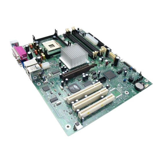
Page 16: Figure 1. Intel Server Board S875Wp1-E Diagram
TP00182 System Fan 4 Header +12V CPU Power Connector R. Battery C. Processor Socket SATA-A1 through SATA-A4 Connector (S875WP1LX only, slots numbered from left to D. CPU Fan right) DIMM Sockets Chassis Intrusion Header Main Power Connector U. PCI 32/33 Slots 1 – 3 G. -
Page 17: Functional Architecture
ATX12V and EPS12V power supplies have an additional power lead that provides required supplemental power for the Intel Pentium 4 processor. The board will not boot if you do not connect the 20-pin (or 24-pin) and 4-pin (or 8-pin) leads of ATX12V or EPS12V power supplies to the corresponding connectors. -
Page 18: Memory Subsystem
Functional Architecture S875WP1-E TPS 3.1.1.1 Reset Configuration Logic The BIOS determines the processor stepping, cache size, and other processor information through the CPUID instruction. The requirement is for the processor to run at a fixed speed. The processor cannot be programmed to operate at a lower or higher speed. On the S875WP1-E platform, the BIOS is responsible for configuring the processor speed. -
Page 19: Memory Configurations
Note: When using PC2700 (333 MHZ) memory with an 800 MHz system bus frequency processor, the memory channel will be set to 320 MHz. Only DIMMs tested and qualified by Intel or a designated memory test vendor will be supported on the Intel Server Board S875WP1-E. A list of qualified DIMMs will be made available through http://support.intel.com/support/motherboards/server/S875WP1-E/... -
Page 20: Table 4. Characteristics Of Dual/Single Channel Configuration With/Without Dynamic Mode
Functional Architecture S875WP1-E TPS Table 4 summarizes the characteristics of dual and single channel configurations with and without the use of Dynamic Mode. Table 4. Characteristics of Dual/Single Channel Configuration with/without Dynamic Mode Throughput Configuration Characteristics Level Highest Dual Channel with Dynamic Mode All DIMMs matched (Example configurations are shown in Figure 2) Dual Channel without Dynamic Mode... -
Page 21: Figure 2. Examples Of Dual Channel Configuration With Dynamic Mode
Dual Channel Configuration with Dynamic Mode (All DIMMs matched) Channel A - DIMM 0 Channel B - DIMM 0 Example Intel Channel B - DIMM 1 Channel A - DIMM 1 82875P Channel A - DIMM 0 Channel B - DIMM 0... -
Page 22: Figure 3. Example Of Dual Channel Configuration Without Dynamic Mode
Dual Channel Configuration without Dynamic Mode - DIMMs not matched within channel - DIMMs match Channel A to Channel B Channel A - DIMM 0 Channel B - DIMM 0 Intel Channel A - DIMM 1 Channel B - DIMM 1 82875P OM15979 Figure 3. -
Page 23: Figure 4. Examples Of Single Channel Configuration With Dynamic Mode
Single Channel Configuration with Dynamic Mode (Single DIMM or DIMMs matched within Channel) Channel A - DIMM 0 Channel B - DIMM 0 Example Intel Channel A - DIMM 1 Channel B - DIMM 1 82875P Channel A - DIMM 0... -
Page 24: Figure 5. Examples Of Single Channel Configuration Without Dynamic Mode
Single Channel Configuration without Dynamic Mode (DIMMs not matched) Channel A - DIMM 0 Channel B - DIMM 0 Example Intel Channel A - DIMM 1 Channel B - DIMM 1 82875P Channel A - DIMM 0 Channel B - DIMM 0... -
Page 25: Intel 875P Chipset
Functional Architecture Intel 875P Chipset The Intel 875P chipset consists of the following devices: • Intel 82875P Memory Controller Hub (MCH) with Accelerated Hub Architecture (AHA) • Intel 82801ER I/O Controller Hub (ICH5-R) with AHA bus • Intel 82802AC (8 Mbit) Firmware Hub (FWH) The MCH is a centralized controller for the system bus, the memory bus, the AGP bus, and the Accelerated Hub Architecture interface. -
Page 26: Agp
The AGP connector Section 5.3 3.2.2 The Intel Server Board S875WP1-E supports up to six USB 2.0 ports, supports Universal Host Controller Interface (UHCI) and Enhanced Host Controller Interface (EHCI), and uses UHCI- and EHCI-compatible drivers. The ICH5-R provides the USB controller for all ports, as shown in Figure 7. The port arrangement is as follows: •... -
Page 27: Ide Interfaces
• Native USB 2.0 support has been tested with Windows* 2000 and Windows XP drivers and is not currently supported by any other operating system. See the Intel server board support website at http://support.intel.com/support/motherboards/server/s875wp1-e possible driver updates for other operating systems. - Page 28 Functional Architecture S875WP1-E TPS NOTE ATA-66 and ATA-100 are faster timings and require a specialized 40-pin, 80-wire cable to reduce reflections, noise, and inductive coupling. The IDE interfaces also support ATAPI devices (such as CD-ROM drives) and ATA devices using the transfer modes. The BIOS supports Logical Block Addressing (LBA) and Extended Cylinder Head Sector (ECHS) translation modes.
-
Page 29: Real-Time Clock, Cmos Sram, And Battery
BIOS Setup program. NOTE If the battery and AC power fail, custom defaults, if previously saved, will be loaded into CMOS RAM at power-on. 3.2.5 Intel 82802AC 8 Megabit Firmware Hub (FWH) The FWH provides the following: • System BIOS program •... -
Page 30: Serial Ata (Sata) Support
S875WP1 includes only two SATA ports through the ICH5-R. Server board with order code S875WP1LX includes an additional four SATA ports using an onboard Promise* Serial ATA controller, for a maximum of six SATA drives. A point-to-point interface is used for host to device connections, unlike IDE which supports a master/slave configuration and two devices per channel. -
Page 31: Sata Raid With Promise Technology Pdc20319
SATA RAID with Promise Technology PDC20319 The Intel Server Board S875WP1LX provides additional four port Serial ATA through the use of the Promise* Technology PDC20319 ASIC. The PDC20319 SATA-150 controller contains four independent SATA channels that share a single 32-bit, 33-MHz PCI bus master interface as a multifunction device, packaged in a 144-pin LQFP. -
Page 32: I/O Controller
3.4.1 Serial Ports The Intel Server Board S875WP1-E has one 9-pin D-sub serial port connector and one 2 x 5 serial port header. The serial port A connector is located in the rear I/O area. The serial port B header is located near the main power connector. The serial ports’ NS16C550-compatible UART supports data transfers at speeds up to 115.2 kbits/sec with BIOS support. -
Page 33: Diskette Drive Controller
S875WP1-E TPS Functional Architecture 3.4.2 Parallel Port The 25-pin D-Sub parallel port connector is located in the rear I/O area. In the BIOS Setup program, the parallel port can be set to the following modes: Output only (PC AT-compatible mode) Bi-directional (PS/2 compatible) •... -
Page 34: Hardware Management Subsystem
S875WP1-E TPS Hardware Management Subsystem The hardware management features enable the Intel Server Board S875WP1-E to be compatible with the Wired for Management (WfM) specification 2.0. The server board complies with DMI specification 2.0 and has several hardware management features, including the... -
Page 35: Chassis Intrusion And Detection
ACPI gives the operating system direct control over the power management and Plug and Play functions of a computer. The use of ACPI with the Intel Server Board S875WP1-E requires an operating system that provides full ACPI support. ACPI features include:... -
Page 36: Table 5. Effects Of Pressing The Power Switch
Functional Architecture S875WP1-E TPS Table 5 lists the system states based on how long the power switch is pressed, depending on how ACPI is configured with an ACPI-aware operating system. Table 5. Effects of Pressing the Power Switch …and the power switch is If the system is in this state…... -
Page 37: Table 7. Wake-Up Devices And Events
S875WP1-E TPS Functional Architecture Processor Targeted System Global States Sleeping States States Device States Power (Note 1) G3 – mechanical No power to the No power D3 – no power for No power to the system. system. wake-up logic, Service can be performed except when safely. - Page 38 3.6.2.1 Power Connector ATX12V or EPS12V compliant power supplies and the Intel Server Board S875WP1-E can turn off the system power through software control. When the system receives the correct command from the operating system, the power supply removes non-standby voltages from the system.
-
Page 39: Table 8. Fan Connector Function/Operation
S875WP1-E TPS Functional Architecture 3.6.2.2 Fan Connectors CAUTION The processor fan must be connected to the processor fan connector, not to a chassis fan connector. Connecting the processor fan to a chassis fan connector may result in onboard component damage that will halt fan operation. Table 8 summarizes the fan connector function/operation. -
Page 40: Standby Power (+5 V) Indicator Led
Functional Architecture S875WP1-E TPS 3.6.2.4 Instantly Available PC Technology CAUTION For Instantly Available* PC technology, the +5 V standby from the power supply must be capable of providing adequate +5 V standby current. Failure to provide adequate standby current when implementing Instantly Available PC technology can damage the power supply. Instantly Available PC technology enables the server board S875WP1-E to enter the ACPI S3 (Suspend-to-RAM) sleep-state. -
Page 41: Figure 8. Location Of The Standby Power Indicator Led (Cr7J1)
S875WP1-E TPS Functional Architecture CR7J1 TP00185 Figure 8. Location of the Standby Power Indicator LED (CR7J1) 3.6.3.1 Wake from USB USB bus activity wakes the computer from an ACPI S1 or S3 state. NOTE Wake from USB requires the use of a USB peripheral that supports it. 3.6.3.2 Wake from PS/2 Devices PS/2 device activity wakes the computer from an ACPI S1 or S3 state. -
Page 42: Table 9. Pci Bus Characteristics
32-KHz clock for the RTC. PCI I/O Subsystem The primary I/O bus for the Intel Server Board S875WP1-E is PCI, with one independent PCI bus. The PCI bus complies with the PCI Local Bus Specification, Rev 2.2. The PCI bus is directed through the Intel 82801ER I/O Controller Hub (ICH5-R). -
Page 43: Table 10. Pci Bus Configuration Ids
Functional Architecture 3.8.1 32-bit, 33-MHz PCI Subsystem All 32-bit, 33-MHz PCI I/O for the Intel Server Board S875WP1-E is directed through the Intel 82801ER I/O Controller Hub (ICH5-R). The PCI bus supports the following embedded devices and connectors: 2D/3D Graphics Accelerator: ATI Rage XL Video Controller SATA controller: Promise Technology PDC20319 •... -
Page 44: Table 11. Video Modes
Functional Architecture S875WP1-E TPS Table 11. Video Modes 2D Mode Refresh Rate (Hz) S875WP1-E 2D Video Mode Support 8 bpp 16 bpp 24 bpp 32 bpp 640x480 60, 72, 75, 90, 100 Supported Supported Supported Supported 800x600 60, 70, 75, 90, 100 Supported Supported Supported... -
Page 45: Network Interface Controller (Nic) Subsystem
Intel 82547EI NIC. When looking at the rear of the chassis, the gigabit NIC is at the left (closest to the video port) and the 10/100Mb NIC is at the right. The Intel Server Board S875WP1-E supports independent disabling of the two NIC controllers using the BIOS Setup menu. -
Page 46: Figure 9. Lan Connector Led Locations
Functional Architecture S875WP1-E TPS Additional features of the NIC subsystem include: PCI bus master interface CSMA/CD protocol engine PCI power management Supports ACPI technology Supports LAN wake capabilities 3.9.1 RJ-45 LAN Connectors with Integrated LEDs Two LEDs are built into each RJ-45 LAN connector (as shown in Figure 9). For the 82562ET NIC, the yellow LED indicates a link to the LAN and the green LED indicates the connection speed. -
Page 47: Table 14. System Memory Map
0377, bits 6:0 7 bits Secondary IDE channel status port 0378 - 037F 8 bytes LPT1 03B0 - 03BB 12 bytes Intel 82875P MCH 03C0 - 03DF 32 bytes Intel 82875P MCH 03E8 - 03EF 8 bytes COM3 03F0 - 03F5... -
Page 48: Table 16. Dma Channels
Maps and Interrupts S875WP1-E TPS Address (hex) Size Description 03F6 1 byte Primary IDE channel command port 03F8 - 03FF 8 bytes COM1 04D0 - 04D1 2 bytes Edge/level triggered PIC LPTn + 400 8 bytes ECP port, LPTn base address + 400h 0CF8 - 0CFB (Note 2) 4 bytes... -
Page 49: Table 17. Pci Configuration Space Map
Table 17. PCI Configuration Space Map Device Function Number (hex) Number (hex) Number (hex) Description Memory controller of Intel 82875P component Host to AGP bridge (virtual P2P) Hub link to PCI bridge Intel 82801ER ICH5-R PCI-to-LPC bridge IDE controller SMBus controller AC ’97 audio controller AC ’97 modem controller (optional) -
Page 50: Table 18. Interrupts
Maps and Interrupts S875WP1-E TPS Interrupts The interrupts can be routed through the Advanced Programmable Interrupt Controller (APIC) portion of the ICH5-R component. The APIC is supported in Windows 2000 Server and Windows XP and supports a total of 24 interrupts. Table 18. -
Page 51: Table 19. Pci Interrupt Routing Map
S875WP1-E TPS Maps and Interrupts PCI Interrupt Routing Map This section describes interrupt sharing and how the interrupt signals are connected between the PCI bus connectors and onboard PCI devices. The PCI specification specifies how interrupts can be shared between devices attached to the PCI bus. In most cases, the small amount of latency added by interrupt sharing does not affect the operation or throughput of the devices. -
Page 52: Table 20. Power Connector Pin-Out (J2J2)
Connectors and Jumper Blocks S875WP1-E TPS Connectors and Jumper Blocks Power Connectors The main power supply connection is obtained using either the 20-pin connector from an ATX12V power supply, or the 24-pin connector from an EPS12V power supply. The following table defines the pin-outs of the connector (For a 20-pin connector, the first 20 pins apply). -
Page 53: Table 22. Auxiliary Power Connector (J4J1)
S875WP1-E TPS Connectors and Jumper Blocks Table 22. Auxiliary Power Connector (J4J1) Signal SMB_CLK_MAIN_CON SMB_DATA_MAIN_CON PS_ALERT# 3.3V PCI Bus Connectors Table 23. PCI Bus Connectors Signal Name Signal Name Signal Name Signal Name Ground (TRST#) -12 V AD16 AD17 (See Note) +12 V Ground (TCK) +3.3 V... -
Page 54: Table 24. Agp Connector
Connectors and Jumper Blocks S875WP1-E TPS Signal Name Signal Name Signal Name Signal Name Ground AD25 AD04 AD05 AD24 +3.3 V Ground AD03 IDSEL C/BE3# AD02 Ground +3.3 V AD23 AD00 AD01 AD22 Ground +5 V (I/O) +5 V (I/O) AD20 AD21 REQ64#... -
Page 55: Table 25. High-Density Front Panel 34-Pin Header Pin Out (J7J1)
S875WP1-E TPS Connectors and Jumper Blocks Signal Name Signal Name Signal Name Signal Name Vcc3.3 Vcc3.3 Vddq Vddq AD30 AD31 AD_STB0# AD_STB0 AD28 AD29 Vcc3.3 Vcc3.3 Ground Ground AD26 AD27 AD24 AD25 Ground Ground Vddq Vddq AD_STB1# AD_STB1 C/BE3# AD23 VRREFG_C VREFC_G NOTE... -
Page 56: Table 26. Vga Connector Pin-Out (J3A1)
VSYNC (vertical sync) V_MONID2 NIC /USB Connector The Intel Server Board S875WP1-E supports two Magjack3* connectors (dual USB + RJ45). The following table details the pin out of the connector. Table 27. Magjack3 Connector (dual USB + RJ45, Gbe) Pin Out (JA4A1) -
Page 57: Table 28. Magjack3 Connector (Dual Usb + Rj45, 10/100) Pin Out (Ja5A1)
LAN_RDN SATA/SATA RAID Connectors The S875WP1-E board provides two (S875WP1) or six (S875WP1LX) SATA/SATA RAID connectors. The pin out for all connectors is identical and is listed in the following table. Table 29. SATA 7-pin Connectors Pin Out (J9E1, J9F1, J9G1, J9H1, J9H2, J9J2) -
Page 58: Table 30. Ich5-R Ide 40-Pin Connector Pin Out (J5J1, J6J1)
Connectors and Jumper Blocks S875WP1-E TPS ICH5-R IDE Connectors The S875WP1-E board provides two 40-pin, low-density ICH5-R IDE connectors. The pin out for both connectors is identical and is listed in the following table. Table 30. ICH5-R IDE 40-pin Connector Pin Out (J5J1, J6J1) Signal Name Signal Name Reset IDE... -
Page 59: Table 32. 34-Pin Floppy Connector Pin Out (J3J1)
DSKCHG# (Diskette Change) 5.11 Serial Port Connector The Intel Server Board S875WP1-E has one 9-pin D-sub serial port connector and one 2 x 5 serial port connector. The following tables detail the pin outs of these two ports. Table 33. 9-pin Serial A Port Pin Out (J2A1) -
Page 60: Table 34. 10-Pin Header Serial B Port Pin Out (J6J4)
Connectors and Jumper Blocks S875WP1-E TPS Table 34. 10-pin Header Serial B Port Pin Out (J6J4) Signal Name DCD (Data Carrier Detect) RXD (Receive Data) TXD (Transmit Data) DTR (Data Terminal Ready) DSR (Data Set Ready) RTS (Request to Send) CTS (Clear to Send) RI (Ring Indicator) 5.12 Keyboard and Mouse Connector... -
Page 61: Miscellaneous Headers
5.13.1 Fan Headers The Intel Server Board S875WP1-E provides four 3-pin fan headers. All fans use direct 12 volts. Four of the five fans, labeled “CPU_FAN”, “SYSFAN1”, “SYSFAN2” and “SYSFAN4” are wired to a fan tachometer input of the Hardware Management ASIC. The third system fan, labeled “SYSFAN3”... -
Page 62: Table 38. Clear Cmos Jumper Settings (J8G1)
Connectors and Jumper Blocks S875WP1-E TPS For information about Refer to How to access the BIOS Setup program Section 7 BIOS recovery Section 6.6 5.15 Clear CMOS Jumper CAUTION Do not move any jumpers with the power on. Always turn off the power and unplug the power cord from the computer before changing a jumper setting. -
Page 63: Bios Flash Memory Organization
BIOS Features BIOS Features The Intel Server Board S875WP1-E uses an Intel/AMI* BIOS that is stored in the Firmware Hub (FWH) and can be updated using a disk-based program. The FWH contains the BIOS Setup program, POST, the PCI auto-configuration utility, and Plug and Play support. -
Page 64: Pci Ide Support
BIOS Features S875WP1-E TPS 6.2.2 PCI IDE Support If Auto is selected from the BIOS Setup program, the BIOS automatically sets up the two PCI IDE connectors with independent I/O channel support. The IDE interface supports hard drives up to ATA-66/100 and recognizes any ATAPI compliant devices, including CD-ROM drives, tape drives, and Ultra DMA drives (see Section 3.2.3). -
Page 65: Legacy Usb Support
S875WP1-E TPS BIOS Features Non-Plug and Play operating systems, such as Windows NT, require an additional interface for obtaining the SMBIOS information. The BIOS supports an SMBIOS table interface for such operating systems. Using this support, an SMBIOS service-level application running on a non-Plug and Play operating system can obtain the SMBIOS information. -
Page 66: Bios Updates
BIOS Features S875WP1-E TPS BIOS Updates The BIOS can be updated using either of the following utilities, which are available on the Intel World Wide Web site: • ® Intel Express BIOS update utility, which enables automated updating while in the Windows environment. -
Page 67: Recovering Bios Data
To create a BIOS recovery diskette, a bootable diskette must be created and the BIOS update files copied to it. BIOS upgrades and the Intel Flash Memory Update Utility are available from Intel Customer Support through the Intel World Wide Web site. -
Page 68: Booting Without Attached Devices
BIOS Features S875WP1-E TPS 6.7.2 Booting Without Attached Devices For use in embedded applications, the BIOS has been designed so that after passing the POST, the operating system loader is invoked even if the following devices are not present: Video adapter Keyboard •... -
Page 69: Intel Rapid Bios Boot
It is possible to optimize the boot process to the point where the system boots so quickly that the Intel logo screen (or a custom logo splash screen) will not be seen. Monitors and hard disk drives with minimum initialization times can also contribute to a boot time that might be so fast that necessary logo screens and POST messages cannot be seen. -
Page 70: Table 39. Supervisor And User Password Functions
BIOS Features S875WP1-E TPS • If only the supervisor password is set, pressing the <Enter> key at the password prompt of the BIOS Setup program allows the user restricted access to Setup. • If both the supervisor and user passwords are set, users can enter either the supervisor password or the user password to access Setup. -
Page 71: Table 40. Bios Setup Program Menu Bar
S875WP1-E TPS BIOS Setup Program BIOS Setup Program The BIOS Setup program can be used to view and change the BIOS settings for the computer. The BIOS Setup program is accessed by pressing the <F2> key after the Power-On Self-Test (POST) memory test begins and before the operating system boot begins. -
Page 72: Table 42. Maintenance Menu
BIOS Setup Program S875WP1-E TPS 7.1.1 Maintenance Menu This menu is used to clear passwords and to access processor information. Setup only displays this menu when the BIOS Configuration jumper is in the configure mode. See page Error! Bookmark not defined. for information about setting the configure mode. To access this menu, select Maintenance on the menu bar at the top of the screen. - Page 73 Set current time. Use the Tab key to navigate fields second • Day of week System Date Set current date. Use the Tab key to navigate fields. Month/day/year NOTE Additional language support is available. For more information visit Intel’s support web site at: www.support.intel.com/support/motherboards/server/S875WP1-E Revision 4.0...
-
Page 74: Table 44. Advanced Menu
BIOS Setup Program S875WP1-E TPS 7.1.3 Advanced Menu To access this menu, select Advanced on the menu bar at the top of the screen. Maintenance Main Advanced Security Power Boot Exit PCI Configuration Boot Configuration Peripheral Configuration Drive Configuration Floppy Configuration Event Log Configuration Video Configuration USB Configuration... -
Page 75: Table 45. Pci Configuration Submenu
S875WP1-E TPS BIOS Setup Program 7.1.3.1 PCI Configuration Submenu To access this submenu, select Advanced on the menu bar, then PCI Configuration. Advanced Maintenance Main Security Power Boot Exit PCI Configuration Boot Configuration Peripheral Configuration Drive Configuration Floppy Configuration Event Log Configuration Video Configuration USB Configuration Chipset Configuration... -
Page 76: Table 46. Boot Configuration Submenu
BIOS Setup Program S875WP1-E TPS 7.1.3.2 Boot Configuration Submenu To access this submenu, select Advanced on the menu bar, then Boot Configuration. Advanced Maintenance Main Security Power Boot Exit PCI Configuration Boot Configuration Peripheral Configuration Drive Configuration Floppy Configuration Event Log Configuration Video Configuration USB Configuration Chipset Configuration... -
Page 77: Table 47. Peripheral Configuration Submenu
S875WP1-E TPS BIOS Setup Program 7.1.3.3 Peripheral Configuration Submenu To access this submenu, select Advanced on the menu bar, then Peripheral Configuration. Advanced Maintenance Main Security Power Boot Exit PCI Configuration Boot Configuration Peripheral Configuration Drive Configuration Floppy Configuration Event Log Configuration Video Configuration USB Configuration Chipset Configuration... - Page 78 BIOS Setup Program S875WP1-E TPS Feature Options Description • 3F8 Base I/O address This option is displayed only if Serial Port B is set to Enabled. • 2F8 (default) Specifies the base I/O address for serial port B. • 3E8 •...
-
Page 79: Table 48. Drive Configuration Submenu
S875WP1-E TPS BIOS Setup Program 7.1.3.4 Drive Configuration Submenu To access this submenu, select Advanced on the menu bar, then Drive Configuration. Advanced Maintenance Main Security Power Boot Exit PCI Configuration Boot Configuration Peripheral Configuration Drive Configuration Floppy Configuration Event Log Configuration Video Configuration USB Configuration Chipset Configuration... - Page 80 • 9 Seconds • 12 Seconds • 15 Seconds • 21 Seconds • 30 Seconds • Disabled (default) Intel (R) RAID Technology • Enabled SATA Port -0 Select to display sub- Reports type of connected SATA device. When selected, displays menu SATA Port-0 submenu.
-
Page 81: Table 49. Primary/Secondary Master/Slave Submenus
S875WP1-E TPS BIOS Setup Program Table 49. Primary/Secondary Master/Slave Submenus Feature Options Description Drive Installed No options Displays the type of drive installed. • User Type Specifies the drive configuration. • Auto (default) User allows capabilities to be changed. Auto fills-in capabilities from the device. Maximum Capacity No options Displays the capacity of the drive. -
Page 82: Table 50. Floppy Configuration Submenu
BIOS Setup Program S875WP1-E TPS 7.1.3.5 Floppy Configuration Submenu To access this menu, select Advanced on the menu bar, then Floppy Configuration. Advanced Maintenance Main Security Power Boot Exit PCI Configuration Boot Configuration Peripheral Configuration Drive Configuration Floppy Configuration Event Log Configuration Video Configuration USB Configuration Chipset Configuration... -
Page 83: Table 51. Event Log Configuration Submenu
S875WP1-E TPS BIOS Setup Program 7.1.3.6 Event Log Configuration Submenu To access this menu, select Advanced on the menu bar, then Event Log Configuration. Advanced Maintenance Main Security Power Boot Exit PCI Configuration Boot Configuration Peripheral Configuration Drive Configuration Floppy Configuration Event Log Configuration Video Configuration USB Configuration... -
Page 84: Table 52. Video Configuration Submenu
BIOS Setup Program S875WP1-E TPS 7.1.3.7 Video Configuration Submenu To access this menu, select Advanced on the menu bar, then Video Configuration. Advanced Maintenance Main Security Power Boot Exit PCI Configuration Boot Configuration Peripheral Configuration Drive Configuration Floppy Configuration Event Log Configuration Video Configuration USB Configuration Chipset Configuration... -
Page 85: Table 53. Usb Configuration Submenu
S875WP1-E TPS BIOS Setup Program 7.1.3.8 USB Configuration Submenu To access this menu, select Advanced on the menu bar, then USB Configuration. Advanced Maintenance Main Security Power Boot Exit PCI Configuration Boot Configuration Peripheral Configuration Drive Configuration Floppy Configuration Event Log Configuration Video Configuration USB Configuration Chipset Configuration... -
Page 86: Table 54. Chipset Configuration Submenu
BIOS Setup Program S875WP1-E TPS 7.1.3.9 Chipset Configuration Submenu To access this menu, select Advanced on the menu bar, then Chipset Configuration. Advanced Maintenance Main Security Power Boot Exit PCI Configuration Boot Configuration Peripheral Configuration Drive Configuration Floppy Configuration Event Log Configuration Video Configuration USB Configuration Chipset Configuration... - Page 87 S875WP1-E TPS BIOS Setup Program Feature Options Description • Auto (default) SDRAM Timing Control This option is available only if User Defined is selected as the Extended Configuration option. • Manual – Aggressive Auto: Timings are programmed according to the memory •...
-
Page 88: Table 55. Fan Control Configuration Submenu
BIOS Setup Program S875WP1-E TPS 7.1.3.10 Fan Control Configuration Submenu To access this menu, select Advanced on the menu bar, then Fan Control Configuration. Advanced Maintenance Main Security Power Boot Exit PCI Configuration Boot Configuration Peripheral Configuration Drive Configuration Floppy Configuration Event Log Configuration Video Configuration USB Configuration... -
Page 89: Table 56. Hardware Monitoring Submenu
S875WP1-E TPS BIOS Setup Program 7.1.3.11 Hardware Monitoring Submenu To access this menu, select Advanced on the menu bar, then Hardware Monitoring. Advanced Maintenance Main Security Power Boot Exit PCI Configuration Boot Configuration Peripheral Configuration Drive Configuration Floppy Configuration Event Log Configuration Video Configuration USB Configuration Chipset Configuration... -
Page 90: Table 57. Remote Access Configuration Submenu
BIOS Setup Program S875WP1-E TPS 7.1.3.12 Remote Access Configuration Submenu To access this menu, select Advanced on the menu bar, then Remote Access Configuration. Advanced Maintenance Main Security Power Boot Exit PCI Configuration Boot Configuration Peripheral Configuration Drive Configuration Floppy Configuration Event Log Configuration Video Configuration USB Configuration... -
Page 91: Table 58. Security Menu
S875WP1-E TPS BIOS Setup Program 7.1.4 Security Menu To access this menu, select Security from the menu bar at the top of the screen. Maintenance Main Advanced Security Power Boot Exit The menu represented by Table 58 is for setting passwords and security features. Table 58. -
Page 92: Table 59. Power Menu
BIOS Setup Program S875WP1-E TPS 7.1.5 Power Menu To access this menu, select Power from the menu bar at the top of the screen. Maintenance Main Advanced Security Power Boot Exit ACPI The menu represented in Table 59 is for setting the power management features. Table 59. -
Page 93: Table 61. Boot Menu
Mode • Disabled • Disabled ® Enables the computer to boot without running certain POST tests. Intel Rapid BIOS Boot • Enabled (default) • Disabled Scan User Flash Area Enables the BIOS to scan the flash memory for user binary files that are executed at boot time. -
Page 94: Table 62. Boot Device Priority Submenu
Press <Enter> to set the selection as the intended boot • Intel (Note 1) ® Boot Device UNDI, PXE device. • Disabled The default settings for the first through fourth boot devices are, respectively: • Removable Dev. • Hard Drive • ATAPI CD-ROM • Intel UNDI, PXE-2.0 Revision 4.0... -
Page 95: Table 63. Hard Disk Drives Submenu
S875WP1-E TPS BIOS Setup Program 7.1.6.2 Hard Disk Drives Submenu To access this menu, select Boot on the menu bar, then Hard Disk Drives. Maintenance Main Advanced Security Power Boot Exit Boot Device Priority Hard Disk Drives Removable Devices ATAPI CDROM Drives The submenu represented in Table 63 is for setting hard disk drive priority. -
Page 96: Table 64. Removable Devices Submenu
BIOS Setup Program S875WP1-E TPS 7.1.6.3 Removable Devices Submenu To access this menu, select Boot on the menu bar, then Removable Devices. Maintenance Main Advanced Security Power Boot Exit Boot Device Priority Hard Disk Drives Removable Devices ATAPI CDROM Drives The submenu represented in Table 64 is for setting removable device priority. -
Page 97: Table 65. Atapi Cdrom Drives Submenu
S875WP1-E TPS BIOS Setup Program 7.1.6.4 ATAPI CDROM Drives Submenu To access this menu, select Boot on the menu bar, then ATAPI CDROM Drives. Maintenance Main Advanced Security Power Boot Exit Boot Device Priority Hard Disk Drives Removable Devices ATAPI CDROM Drives The submenu represented in Table 65 is for setting ATAPI CDROM drive priority. -
Page 98: Error Sources And Types
Error Reporting and Handling S875WP1-E TPS Error Reporting and Handling This section documents the types of system bus error conditions monitored by the Intel Server Board S875WP1-E. Error Sources and Types One of the major requirements of server management is to correctly and consistently handle system errors. -
Page 99: Single-Bit Ecc Error Throttling Prevention
POST errors are logged in to the SEL. The error codes are defined by Intel and, whenever possible, are backward compatible with error codes used on earlier platforms. -
Page 100: Table 67. Bios Error Messages
Error Reporting and Handling S875WP1-E TPS 8.2.1 BIOS Error Messages During POST, if an error is detected, the BIOS will display an error code and message to the screen. The following table defines POST error codes and their associated messages. The BIOS prompts the user to press a key in case of serious errors. -
Page 101: Table 68. Uncompressed Init Code Checkpoints
S875WP1-E TPS Error Reporting and Handling Error Message Explanation Off Board Parity Error A parity error occurred on an off-board card. This error is followed by an address. On Board Parity Error A parity error occurred in on-board memory. This error is followed by an address. -
Page 102: Table 69 Boot Block Recovery Code Checkpoints
Shadow RAM and give control to recovery code in F000 Shadow RAM. Initialize interrupt vector tables, initialize system timer, initialize DMA controller and interrupt controller. Initialize extra (Intel Recovery) Module. Initialize floppy drive. Try to boot from floppy. If reading of boot sector is successful, give control to boot sector code. - Page 103 S875WP1-E TPS Error Reporting and Handling Code Description of POST Operation EGA/VGA not found. Display memory R/W test about to begin. Display memory R/W test passed. About to look for the retrace checking. Display memory R/W test or retrace checking failed. To do alternate Display memory R/W test. Alternate Display memory R/W test passed.
- Page 104 Error Reporting and Handling S875WP1-E TPS Code Description of POST Operation Lock-key checking over. To check for memory size mismatch with CMOS. Memory size check done. To display soft error and check for password or bypass setup. Password checked. About to do programming before setup. Programming before setup complete.
-
Page 105: Table 71. Bios Beep Codes
S875WP1-E TPS Error Reporting and Handling followed by two short tones) during POST if the video configuration fails (a faulty video card or no card installed) or if an external ROM module does not properly checksum to zero. An external ROM module (for example, a video BIOS) can also issue audible errors, usually consisting of one long tone followed by a series of short tones. -
Page 106: Table 72. Bus Initialization Checkpoints
Error Reporting and Handling S875WP1-E TPS Bus Initialization Checkpoints The system BIOS gives control to the different buses at several checkpoints to do various tasks. Table 72 describes the bus initialization checkpoints. Table 72. Bus Initialization Checkpoints Checkpoint Description Different buses init (system, static, and output devices) to start if present. Different buses init (input, IPL, and general devices) to start if present. -
Page 107: Table 75. Absolute Maximum Ratings
VDD means supply voltage for the device. S875WP1-E Power Budget The following table shows the power consumed on each supply line for a Intel Server Board S875WP1-E that is configured with one Intel Pentium 4 processor (pulling max current), all... -
Page 108: Product Regulatory Compliance
The S875WP1-E has been has been tested and verified to comply with the following electromagnetic compatibility (EMC) regulations when installed in a compatible Intel host system. For information on compatible host system(s), contact your local Intel representative. FCC (Class A Verification) – Radiated & Conducted Emissions (USA) ICES-003 (Class A) –... -
Page 109: Product Regulatory Compliance Markings
(1) this device may not cause harmful interference, and (2) this device must accept any interference received, including interference that may cause undesired operation. For questions related to the EMC performance of this product, contact: Intel Corporation 5200 N.E. Elam Young Parkway Hillsboro, OR 97124 1-800-628-8686 Revision 4.0... -
Page 110: Industry Canada (Ices-003)
General Specifications S875WP1-E TPS This equipment has been tested and found to comply with the limits for a Class A digital device, pursuant to Part 15 of the FCC Rules. These limits are designed to provide reasonable protection against harmful interference in a residential installation. This equipment generates, uses, and can radiate radio frequency energy and, if not installed and used in accordance with the instructions, may cause harmful interference to radio communications. -
Page 111: Korean Rrl Compliance
MIC logo to illustrate compliance. The English translation for the above is as follows: 1. Type of Equipment (Model Name): S875WP1-E 2. Certification No.: Contact Intel Representative 3. Name of Certification Recipient: Intel 4. Date of Manufacturer: Marked on Product 5. -
Page 112: Calculated Mean Time Between Failures (Mtbf)
Hävitä käytetty paristo valmistajan ohjeiden mukaisesti. Calculated Mean Time Between Failures (MTBF) The MTBF (Mean Time Between Failures) for the Intel Server Board S875WP1-E as configured from the factory is shown in the table below. Product Code... -
Page 113: Figure 10. S875Wp1-E Server Board Mechanical Drawing
S875WP1-E TPS General Specifications Figure 10. S875WP1-E Server Board Mechanical Drawing Revision 4.0... -
Page 114: Figure 11. Intel Server Board S875Wp1-E I/O Shield Drawing
The following figure shows the Intel Server Board S875WP1-E general-purpose chassis I/O shield mechanical drawing. If the Intel Server Board S875WP1-E is used in a 1U chassis, the user will need to obtain the I/O shield directly from the chassis vendor. - Page 115 Field replaceable unit 1024 MB. GPIO General purpose I/O GUID Globally Unique ID Hertz (1 cycle/second) Hardware Design Guide Inter-integrated circuit bus ® Intel architecture ICMB Intelligent Chassis Management Bus IERR Internal error Inter Module Bus Internet Protocol Interrupt Request In-target probe...
- Page 116 Glossary S875WP1-E TPS Term Definition Low pin count Least Significant Bit 1024 KB Multi-Bit Error milliseconds Most Significant Bit MTBF Mean Time Between Failures multiplexor Network Interface Card Non-maskable Interrupt Original equipment manufacturer Unit of electrical resistance PBGA Pin Ball Grid Array PERR Parity Error Programmable I/O...
- Page 117 S875WP1-E TPS Glossary Term Definition Universal Serial Bus Video Graphic Adapter Voltage Identification Voltage Regulator Module Word 16-bit quantity Zero Channel RAID Revision 4.0...
Need help?
Do you have a question about the S875WP1LX and is the answer not in the manual?
Questions and answers