
Related Manuals for ADLINK Technology COM Express cExpress-BL


Summary of Contents for ADLINK Technology COM Express cExpress-BL
- Page 1 cExpress-BL User’s Manual Manual Revision: Revision Date: January 2, 2018 Part Number: 50-1J061-1020 Leading EDGE COMPUTING...
-
Page 2: Revision History
Revision History Revision Description Date 1.00 Initial release 2015-05-07 1.01 Update CPU, COM port, power mgmt. specifications; correct LVDS pinout; correct audio, LVDS, 2015-07-22 eDP, GbE, SATA, SPI, Fan, SMBus, DDI signal descriptions; update BIOS setup Update switch information 2018-01-02 Page 2... -
Page 3: Preface
Preface Copyright 2015-18 ADLINK Technology, Inc. This document contains proprietary information protected by copyright. All rights are reserved. No part of this manual may be reproduced by any mechanical, electronic, or other means in any form without prior written permission of the manufacturer. -
Page 4: Table Of Contents
Table of Contents Revision History ......................2 Preface..........................3 Introduction ......................6 Specifications....................... 7 2.1. Core System..........................7 2.2. Expansion Busses ........................7 2.3. Video ............................7 2.4. Audio ............................8 2.5. LAN ............................8 2.6. Multi I/O and Storage........................8 2.7. Serial I/O on Module .........................8 2.8. - Page 5 cExpress-BL Smart Embedded Management Agent (SEMA) ..........38 5.1. Board Specific SEMA Functions....................39 System Resources....................41 6.1. System Memory Map ......................41 6.2. Direct Memory Access Channels.................... 41 6.3. I/O Map ..........................42 6.4. Interrupt Request (IRQ) Lines....................44 6.5.
-
Page 6: Introduction
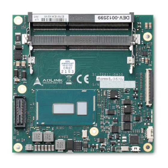
1. Introduction The cExpress-BL is a COM Express® COM.0 R2.1 Type 6 Compact size module featuring the 64-bit 5th Generation Intel® Core™ i7/i5/i3 and Intel® Celeron® Ultra-Low TDP processors (formerly “Broadwell-U”) with CPU, memory controller, graphics processor and I/O hub on a single chip. -
Page 7: Specifications
cExpress-BL 2. Specifications 2.1. Core System CPU: 5th Generation Intel® Core™ processor SoC (formerly “Broadwell-U”) • Intel® Core™ i7-5650U 2.2 GHz (3.1 GHz Turbo), 15W (2C/GT3) • Intel® Core™ i5-5350U 1.8 GHz (2.7 GHz Turbo), 15W (2C/GT3) • Intel® Core™ i3-5010U 2.1 GHz (no Turbo), 15W (2C/GT2) •... -
Page 8: Audio
2.4. Audio Integrated: Intel® HD Audio integrated on SoC Codec: Realtek ALC886 on Express-BASE6 Reference Carrier Board 2.5. Integrated: MAC integrated on SoC Intel PHY: Intel® Ethernet Controller i218LM Interface: 10/100/1000 GbE connection 2.6. Multi I/O and Storage I/O Hub: Integrated on SOC USB: 2x USB 3.0 ports (USB0,1) and 6x USB 2.0 ports (USB2,3,4,5,6,7) SATA: 4x SATA 6Gb/s ports GPIO: 4 GPO and 4 GPI... -
Page 9: Debug
cExpress-BL 2.10. Debug 40-pin flat cable connector to be used with DB-40 debug module Supports: BIOS POST code LED, BMC access, SPI BIOS flashing, power testpoints, debug LEDs 60-pin XDP header for ICE debug of CPU/chipset 2.11. Power Specifications Power Modes: AT and ATX mode (AT mode startup controlled by SEMA Board Controller) Standard Voltage Input: ATX = 12V±5% / 5Vsb ±5% or AT = 12V±5% Wide Voltage Input:... -
Page 10: Functional Diagram
2.16. Functional Diagram Page 10... -
Page 11: Mechanical Drawing
cExpress-BL 2.17. Mechanical Drawing connectors on bottom side Top View Side View All tolerances ± 0.05 mm Other tolerances ± 0.2 mm Dimensions: mm Page 11... -
Page 12: Pinouts And Signal Descriptions
3. Pinouts and Signal Descriptions 3.1. AB/CD Pin Definitions The cExpress-BL is a Type 6 module supporting USB 3.0 upgrade signals and DDI channels on the CD connector All pins in the COM Express specification are described, including those not supported on the cExpress-BL. Those not supported on the cExpress-BL module are crossed out. - Page 13 cExpress-BL Row A Row B Row C Row D Name Name Name Name USB6- USB7- DDI1_PAIR3+ DDI3_CTRLCLK_AUX+ USB6+ USB7+ DDI1_PAIR3- DDI3_CTRLDATA_AUX- USB_6_7_OC# USB_4_5_OC# RSVD DDI3_DDC_AUX_SEL USB4- USB5- DDI3_PAIR0+ DDI2_PAIR0+ USB4+ USB5+ DDI3_PAIR0- DDI2_PAIR0- GND (FIXED) GND (FIXED) GND (FIXED) GND (FIXED) USB2- USB3- DDI3_PAIR1+...
- Page 14 Row A Row B Row C Row D Name Name Name Name GND (FIXED) GND (FIXED) GND (FIXED) GND (FIXED) LVDS_A_CK+ LVDS_B_CK+ PEG_RX9+ PEG_TX9+ (eDP_TX3+) LVDS_A_CK- LVDS_B_CK- PEG_RX9- PEG_TX9- (eDP_TX3-) LVDS_I2C_CK LVDS_BKLT_CTRL RSVD RSVD /eDP_AUX+ * /eDP_BKLT_CTRL * LVDS_I2C_DAT VCC_5V_SBY /eDP_AUX- * VCC_5V_SBY PEG_RX10+...
-
Page 15: Signal Description Terminology
cExpress-BL 3.2. Signal Description Terminology The following terms are used in the COM Express AB/CD Signal Descriptions below. Input to the Module Output from the Module Bi-directional input/output signal Open drain output I 3.3V Input 3.3V tolerant I 5V Input 5V tolerant O 3.3V Output 3.3V signal level O 5V... -
Page 16: Ab Signal Descriptions
3.3. AB Signal Descriptions 3.3.1. Audio Signals Signal Pin # Description PU/PD Comment AC_RST# / Reset output to codec, active low. O 3.3VSB VSB because PCH uses suspend HDA_RST# power for RESET AC_SYNC / Sample-synchronization signal to the codec(s). O 3.3V HDA_SYNC AC_BITCLK / Serial data clock generated by the external... - Page 17 cExpress-BL 3.3.3. LVDS/eDP Signal Pin # Description PU/PD Comment LVDS_A0+ LVDS Channel A differential pairs O LVDS LVDS is default. LVDS_A0- (through eDP to LVDS LVDS_A1+ bridge) LVDS_A1- LVDS_A2+ Note: eDP support is a LVDS_A2- - LVDS_A3+ BOM option LVDS_A3- LVDS_A_CK+ LVDS Channel A differential clock O LVDS...
- Page 18 3.3.4. Gigabit Ethernet Gigabit Ethernet Pin # Description PU/PD Comment GBE0_MDI0+ Gigabit Ethernet Controller 0: Media Dependent Interface Differential Pairs I/O Analog Twisted pair GBE0_MDI0- 0, 1, 2, 3. The MDI can operate in 1000, 100, and 10Mbit/sec modes. signals for GBE0_MDI1+ Some pairs are unused in some modes according to the following: external...
- Page 19 cExpress-BL 3.3.6. PCI Express Signal Pin # Description PU/PD Comment PCIE_TX0+ PCI Express channel 0, Transmit Output differential O PCIE AC coupled on Module PCIE_TX0- pair. PCIE_RX0+ PCI Express channel 0, Receive Input differential I PCIE AC coupled off Module PCIE_RX0- pair.
- Page 20 3.3.9. Signal Pin # Description PU/PD Comment USB0+ USB differential data pairs for Port 0 I/O 3.3VSB USB 1.1/ 2.0 compliant USB0- USB1+ USB differential data pairs for Port 1 I/O 3.3VSB USB 1.1/ 2.0 compliant USB1- USB2+ USB differential data pairs for Port 1 I/O 3.3VSB USB 1.1/ 2.0 compliant USB2-...
- Page 21 cExpress-BL 3.3.10. USB Root Segmentation 3.3.11. SPI (BIOS only) Signal Pin # Description PU/PD Comment SPI_CS# Chip select for Carrier Board SPI BIOS Flash. O 3.3VSB PU 10K 3.3VSB SPI_MISO Data in to module from carrier board SPI BIOS flash. I 3.3VSB SPI_MOSI Data out from module to carrier board SPI BIOS flash.
- Page 22 3.3.12. Miscellaneous Signal Pin # Description PU/PD Comment SPKR Output for audio enunciator, the “speaker” in PC-AT O 3.3V systems Output indicating that a watchdog time-out event has O 3.3V occurred. THRM# Input from off-module temp sensor indicating an over- I 3.3V temp situation.
- Page 23 cExpress-BL Signal Pin # Description PU/PD Comment GPO[3] General purpose output pins. O 3.3V PU 10K 3.3V After hardware RESET output low GPI[0] General purpose input pins. I 3.3V PU 10K 3.3V Pulled high internally on the module. GPI[1] General purpose input pins. I 3.3V PU 10K 3.3V Pulled high internally on the module.
- Page 24 Signal Pin # Description PU/PD Comment BATLOW# Battery low input. This signal may be driven low by external circuitry to I 3.3VSB PU 10k signal that the system battery is low, or may be used to signal some other 3.3VSB external power-management event.
-
Page 25: Cd Signal Descriptions
cExpress-BL 3.4. CD Signal Descriptions 3.4.1. USB 3.0 extension Signal Description PU/PD Comment USB_SSRX0- Additional Receive signal differential pairs for the I PCIE USB_SSRX0+ SuperSpeed USB data path on USB0 USB_SSTX0- Additional Transmit signal differential pairs for the O PCIE AC coupled on Module USB_SSTX0+ SuperSpeed USB data path on USB0... - Page 26 3.4.3. DDI Channels DDI 1 Signal Description PU/PD Comment DDI1_PAIR0+ Digital Display Interface1 differential pairs O PCIE DDI1_PAIR0- DDI1_PAIR1+ DDI1_PAIR1- DDI1_PAIR2+ DDI1_PAIR2- DDI1_PAIR3+ DDI1_PAIR3- DDI1_PAIR4+ Pair 4 to Pair 6 DDI1_PAIR4- Not supported DDI1_PAIR5+ DDI1_PAIR5- DDI1_PAIR6+ DDI1_PAIR6- DDI1_HPD Digital Display Interface Hot-Plug Detect I PCIE PD 10M DDI1_CTRLCLK_AUX+...
- Page 27 cExpress-BL DDI 2 Signal Description PU/PD Comment DDI2_PAIR0+ Digital Display Interface2 differential pairs DDI2_PAIR0- DDI2_PAIR1+ DDI2_PAIR1- DDI2_PAIR2+ DDI2_PAIR2- DDI2_PAIR3+ DDI2_PAIR3- DDI2_HPD PD 10M DDI2_CTRLCLK_AUX+ IF DDI2_DDC_AUX_SEL is floating I/O PCIe DP2_AUX+ IF DDI2_DDC_AUX_SEL pulled high I/O OD 3.3V HDMI2_CTRLCLK DDI2_CTRLCLK_AUX- IF DDI2_DDC_AUX_SEL is floating I/O PCIe DP2_AUX+...
- Page 28 3.4.4. DDI to DP/HDMI/SDVO Mapping Pin Name HDMI \ DVI DDI1_PAIR0+ DP1_LANE0+ TMDS1_DATA2+ DDI1_PAIR0- DP1_LANE0- TMDS1_DATA2- DDI1_PAIR1+ DP1_LANE1+ TMDS1_DATA1+ DDI1_PAIR1- DP1_LANE1- TMDS1_DATA1- DDI1_PAIR2+ DP1_LANE2+ TMDS1_DATA0+ DDI1_PAIR2- DP1_LANE2- TMDS1_DATA0- DDI1_PAIR3+ DP1_LANE3+ TMDS1_CLK+ DDI1_PAIR3- DP1_LANE3- TMDS1_CLK- DDI1_PAIR4+ Not supported Not supported DDI1_PAIR4- Not supported Not supported DDI1_PAIR5+...
- Page 29 cExpress-BL 3.4.5. PCI Express Graphics x16 (PEG) Signal Description PU/PD Comment PEG_RX0+ PCI Express Graphics transmit differential pairs. I PCIE Not supported PEG_RX0- PEG_RX1+ PEG_RX1- PEG_RX2+ PEG_RX2- PEG_RX3+ PEG_RX3- PEG_RX4+ PEG_RX4- PEG_RX5+ PEG_RX5- PEG_RX6+ PEG_RX6- PEG_RX7+ PEG_RX7- PEG_RX8+ PEG_RX8- PEG_RX9+ PEG_RX9- PEG_RX10+ PEG_RX10-...
- Page 30 Signal Description PU/PD Comment PEG_TX15+ D101 PEG_TX15- D102 PEG_LANE_RV# PCI Express Graphics lane reversal input strap. I 1.05V Not supported Pull low on the Carrier board to reverse lane order. 3.4.6. Module Type Definition Signal Pin # Description Comment TYPE0# The TYPE pins indicate to the Carrier Board the Pin-out Type that is implemented Type 6 TYPE1#...
-
Page 31: Connector Pinouts On Module
cExpress-BL 4. Connector Pinouts on Module This chapter describes connectors and pinouts, LEDs and switches that are used on the module but are not included in the PICMG standard specification Connector and LED Locations 60-pin to CPU BIOS Defaults Reset Switch 40-pin Debug 4-pin... -
Page 32: 40-Pin Debug Connector
4.1. 40-pin Debug Connector FPC Connector Type: FCI 59GF Flex 10042867 Pin Orientation cExpress-BL and the DB40 Debug Module Page 32... - Page 33 cExpress-BL 40-pin Debug Connector Pin Definition on the COM Express Module Interface Signal Remark Pin Interface Signal Remark VCC_SPI_IN SPI Power Input from flash tool BMC Program TXD6 Program to module. HW need add MOS interface interface FET to switch SPI power for SPI (continued) RXD6 SPI_BIOS_CS0#...
-
Page 34: Status Leds
4.2. Status LEDs To facilitate easier maintenance, status LED’s are mounted on the board. LED Descriptions Name Color Connection Function LED1 Blue BMC output Power Sequence Status Code (BMC) Power Changes, RESET (see 5.1.4 Exception Codes below) LED2 Green Power Source 3Vcc LED ON S3/S4/S5 LED OFF... -
Page 35: Xdp Debug Header
cExpress-BL 4.3. XDP Debug header The debug port is a connection into a target-system environment that provides access to JTAG, run control, system control, and observation resources. The XDP target system connector is a Samtec™ 60-pin BSH-030-01 series connector. Pin XDP Signal Target Signal Device XDP Signal... -
Page 36: Fan Connector
4.4. Fan Connector Connector Type: JVE 24W1125A-04M00 Pin Assignment Name Signal Description BMC_FAN_OUT FAN_PWMOUT BMC_FAN_PWM_IN FAN_TACHIN Ground P5V_S 4.5. BIOS Setup Defaults Reset Button To perform a hardware reset of BIOS default settings, perform the following steps: Shut down the system. Press the BIOS Setup Defaults RESET Button continuously and boot up the system. -
Page 37: Bios Select And Mode Configuration Switch
cExpress-BL 4.6. BIOS Select and Mode Configuration Switch BIOS Select and Mode Configuration Switch The module has two BIOS chips and BIOS operation can be configured to "PICMG" and dual-BIOS "Failsafe" modes using the BIOS Select and Mode Configuration Switch, Pin 2. Setting the module to PICMG mode will configure the BIOS chips on the module as SPI0 and SPI1. -
Page 38: Smart Embedded Management Agent (Sema)
5. Smart Embedded Management Agent (SEMA) The onboard microcontroller (BMC) implements power sequencing and Smart Embedded Management Agent (SEMA) functionality. The microcontroller communicates via the System Management Bus with the CPU/chipset. The following functions are implemented: ‧ Total operating hours counter. Counts the number of hours the module has been run in minutes. ‧... -
Page 39: Board Specific Sema Functions
cExpress-BL 5.1. Board Specific SEMA Functions 5.1.1. Voltages The BMC of the cExpress-BL implements a voltage monitor and samples several onboard voltages. The voltages can be read by calling the SEMA function “Get Voltages”. The function returns a 16-bit value divided into high-byte (MSB) and low-byte (LSB). ADC Channel Voltage Name Voltage Formula [V]... - Page 40 5.1.4. Exception Codes In case of an error, the BMC drives a blinking code on the blue Status LED (LED1). The same error code is also reported by the BMC Flags register. The Exception Code is not stored in the Flash Storage and is cleared when the power is removed. Therefore, a “Clear Exception Code”...
-
Page 41: System Resources
cExpress-BL 6. System Resources 6.1. System Memory Map Address Range (decimal) Address Range (hex) Size Description (4GB-2MB) FFE00000 – FFFFFFFF 2 MB High BIOS Area (4GB-18MB) – (4GB-17MB-1) FEE00000 – FEEFFFFF 1 MB MSI Interrupts (4GB-20MB) – (4GB-19MB-1) FEC00000 – FECFFFFF 1 MB APIC Configuration Space 15MB –... -
Page 42: I/O Map
6.3. I/O Map Hex Range Device 000-01F Reserved 020-02D and 030-03F Interrupt controller 1, 8259 equivalent 02E-02F LPC SIO () configuration index/data registers 040-05F Timer, 8254-2 equivalent 060, 062, 064, 066, 068-06F 8742 equivalent (keyboard) 061, 063, 065, 067 NMI control and status 070-07F Real Time Clock Controller( bit 7 -NMI mask) 080-090... - Page 43 cExpress-BL Hex Range Device 3F0-3F7 Available 3F8-3FF Serial port 1 Master PIC Edge/Level Trigger register Slave PIC Edge/Level Trigger register CF8-CFB PCI configuration address register (32 bit I/O only) Reset Control register (8 bit I/O) CFC-CFF PCI configuration data register F040 Smbus base address for SB.
-
Page 44: Interrupt Request (Irq) Lines
6.4. Interrupt Request (IRQ) Lines PIC Mode IRQ# Typical Intterupt Resource Connected to Pin Available Counter 0 Keyboard controller Cascade interrupt from slave PIC Serial Port 2 (COM2) IRQ3 via SERIRQ / PIRQ Note (1) Serial Port 1 (COM1) IRQ4 via SERIRQ / PIRQ Note (1) Parallel Port 2 (LPT2) IRQ5 via SERIRQ / PIRQ... - Page 45 cExpress-BL IRQ# Typical Intterupt Resource Connected to Pin Available Serial Port 4 (COM4) IRQ11 via SERIRQ / PIRQ Note (1) PS/2 Mouse IRQ12 via SERIRQ / PIRQ Note (1) Math Processor Note (1) Primary IDE controller IRQ14 via SERIRQ / PIRQ Note (1) Secondary IDE controller IRQ15 via SERIRQ / PIRQ...
-
Page 46: Pci Configuration Space Map
6.5. PCI Configuration Space Map Device Function Routing Description Number Number Number Intel host Bridge Internal Intel I.G.D Internal HD Audio Device Internal Instel Smart Sound Technology Controller Internal xHCI Controller Internal Intel Serial I/O DMA Controller Internal Intel Serial I/O I2C Controller #0 Internal Intel Serial I/O I2C Controller #1 Internal... -
Page 47: Pci Interrupt Routing Map
cExpress-BL 6.6. PCI Interrupt Routing Map P.E.G Root Audio xHCI ME Controller ME Controller IDE-R Line Port Controller Controller Controller Controller Int0 INTA:16 INTH:23 INTA:16 INTA:16 INTE:20 INTG:22 Int1 INTB:17 INTD:19 Int2 INTC:18 INTC:18 Int3 INTD:19 INTB:17 PCIE port1 PCIE port 2 PCIE port 3 PCIE port 4 PCIE port5... -
Page 48: Bios Setup
7. BIOS Setup 7.1. Menu Structure This section presents the six primary menus of the BIOS Setup Utility. Use the following table as a quick reference for the contents of the BIOS Setup Utility. The subsections in this section describe the submenus and setting options for each menu item. The default setting options are presented in bold, and the function of each setting is described in the right hand column of the respective table. -
Page 49: Main
cExpress-BL 7.2. Main The Main Menu provides read-only information about your system and also allows you to set the System Date and Time. Refer to the tables below the screen shot of this menu for details of the submenus and settings. 7.2.1. - Page 50 7.2.5. Main >System Management > Board Information Board Information Info only SEMA Firmware Read only Display SEMA Firmware. Build Date Read only Display SEMA firmware build date. SEMA Boot loader Read only Display SEMA boot loader. Build Date Read only Display SEMA boot loader build date.
- Page 51 cExpress-BL Feature Options Description V3.30 Read only Display actual voltage of the V3.30. VMEM Read only Display actual voltage of the VMEM. V5.00 Read only Display actual voltage of the V5.00. Read only Display actual voltage of the VIN. AIN7 Read only Display actual voltage of the AIN7.
- Page 52 7.2.9. System Management > LVDS Backlight Feature Options Description LVDS Backlight Info only LVDS Backlight Bright The value range starts by 0 and ends by 255. 7.2.10. System Management > Smart Fan Feature Options Description Smart Fan Info only CPU Smart FanTemperature Source CPU Sensor Select CPU smart fan source.
-
Page 53: Advanced
cExpress-BL 7.3. Advanced This menu contains the settings for most of the user interfaces in the system. 7.3.1. Advanced > CPU Feature Options Description Info only Manufacturer, model, speed CPU Signature Info only Display CPU Signature. Microcode Patch Info only Display Microcode Patch. - Page 54 Feature Options Description CPU C7 Report Disabled Enable / Disable CPU C7 report to OS. CPU C7 CPU C7S C1 State auto undemotion Disabled Un-demotion from Demoted C1 Enabled C3 State auto undemotion Disabled Un-demotion from Demoted C3 Enabled ACPI T State Disabled Enable / Disable ACPI T state support.
- Page 55 cExpress-BL 7.3.3. Advanced > Graphics Feature Options Description Graphics Configuration Info only IGFX VBIOS Version Info only Display VBIOS Version. IGfx Frequency Info only Display IGfx Frequency. Graphics Turbo IMON Current Number entry field Graphics turbo IMON current values supported (14-31). Primary Display Auto Select which of IGFX/PEG/PCI Graphics device should be Primary Display...
- Page 56 Feature Options Description DDI function choose Display Port Select DDI function choose to display port or HDMI. HDMI Primary IGFX Boot Display VBIOS Default Select the Video Device which will be activated during POST LCD Panel Type VBIOS Default Select LCD panel used by Internal Graphics Device by selecting the appropriate setup item.
- Page 57 cExpress-BL Feature Options Description SATA Port Configuration Submenu Software Feature Mask Configuration Info only RAID0 Enabled Enable / Disable RAID0 feature. Disabled RAID1 Enabled Enable / Disable RAID1 feature. Disabled RAID10 Enabled Enable / Disable RAID10 feature. Disabled RAID5 Enabled Enable / Disable RAID5 feature.
- Page 58 Feature Options Description USB Module Version Info only USB Devices Info only X Drive, X Keyboards, X Mouse, X Hubs Legacy USB Support Enabled Enables legacy USB support. Disabled Auto option disables legacy support if no USB devices are connected. Auto Disable option will keep USB devices available only for EFI applications and setup.
- Page 59 cExpress-BL Feature Options Description Network Stack Info only Network Stack Enabled Enable/Disable UEFI network stack. Disabled PCH LAN Controller Enabled Enable / Disable onboard NIC. Disabled Wake on LAN Enabled Enable / Disable integrated LAN to wake the system. (The Wake On LAN Disabled cannot be disabled if ME is on at Sx state.
- Page 60 Feature Options Description 160 PCI Bus Clocks 192 PCI Bus Clocks 224 PCI Bus Clocks 248 PCI Bus Clocks VGA Palette Snoop Disabled Allow PCI cards that do not contain their own VGA color palette to access Enabled the video core’s palette PERR# Generation Disabled Enables or Disables PCI Device to Generate PERR#.
- Page 61 cExpress-BL 7.3.7.1. Advanced > PCI and PCIe > PCH-PCIe Configuration Feature Options Description PCH-PCIe Configuration Info only PCI Express Clock Gating Disable Enable / Disable PCI Express Clock Gating for each root port. Enable DMI Link ASPM Control Disable The control of Active State Power Management on both NB side and SB side of the DMI Link.
- Page 62 Feature Options Description SENFE Disable Enable / Disable Root PCI Express System Error on Non-Fatal Error. Enable SECE Disable Enable / Disable Root PCI Express System Error on Correctable Error. Enable PME SCI Disable Enable / Disable PCI Express PME SCI. Enable Hot Plug Disable...
- Page 63 cExpress-BL Feature Options Description Serial Port 2 Configuration Serial Port Enabled Enable / Disable Serial Port (COM). Disabled IO=2F8h; IRQ=4 Device Settings Fixed configuration of serial port. Auto IO=2F8h; IRQ=3 Change Settings Select an optimal setting for super IO device. IO=3F8h;...
- Page 64 7.3.9. Advanced > ACPI and Power Management Feature Options Description ACPI and Power Management Info only Enable ACPI Auto Configuration Enabled Enables or Disables BIOS ACPI Auto Configuration. Disabled Enable Hibernation Enabled Enables or Disables System ability to Hibernate (OS/S4 Sleep State). This Disabled option may be not effective with some OS.
- Page 65 cExpress-BL Feature Options Description COM4 Info only Console Redirection Enabled Console Redirection Enable or Disable. Disabled Console Redirection Settings Submenu 7.3.11.1. Advanced > Serial Port Console > Console Redirection Feature Options Description Console Redirection Settings Info only Terminal Type VT100 Emulation: ANSI: Extended ASCII char set.
- Page 66 7.3.12. Advanced > ICC Configuration Feature Options Description Turn off unused PCI/PCIe clocks Disabled Disabled: all clocks turned on. Enable Enabled: clocks for empty PCI/PCIe slots will be turned off to save power. Platform must be powered off for changes to take effect. Clock Manipulation Info only ICC Overclocking Lib...
- Page 67 cExpress-BL 7.3.13. Advanced > Thermal Feature Options Description Thermal Info only Automatic Thermal Reporting Enabled Configure _CRT, _PSV and _AC0 automatically based on values Disabled recommended in BWG’s Thermal Reporting for Thermal Management settings. Set to Disabled for manual conmfiguration. Critical Trip Point Disable This value controls the temperature of the ACPI Critical Trip Point - the...
- Page 68 7.3.14.1. Advanced > Miscellaneous > BIOS Security Configuration Feature Options Description SMI Lock Enabled Enable or Disable the SMI Lock Disabled BIOS Lock Enabled Enable or Disable the BIOS lock enable (BLE) bit Disabled GPIO Lock Enabled Enable or Disable the GPIO lockdown Disabled BIOS Interface Lock Enabled...
-
Page 69: Boot
cExpress-BL 7.4. Boot The Boot Menu allows control of Boot features 7.4.1. Boot > Boot Configuration Feature Options Description Boot Configuration Info only Setup Prompt Timeout Enable / Disable the onboard SATA controllers. Bootup NumLock State Select SATA controller mode. Quiet Boot Disabled Enable / Disable the PATA port. -
Page 70: Security
7.5. Security 7.5.1. Security > Password Description Feature Options Description Administrator Password Enter password User Password Enter password HDD Security Configuration: Info only Px: xxxxxxxx Info only 7.6. Save & Exit 7.6.1. Save and Exit > Reset Options Feature Options Description Save Changes and Reset Save changes and reset the... -
Page 71: Bios Checkpoints, Beep Codes
cExpress-BL 8. BIOS Checkpoints, Beep Codes This section of this document lists checkpoints and beep codes generated by AMI Aptio BIOS. The checkpoints defined in this document are inherent to the AMIBIOS generic core, and do not include any chipset or board specific checkpoint definitions. Checkpoints and Beep Codes Definition A checkpoint is either a byte or word value output to I/O port 80h. -
Page 72: Status Code Ranges
8.1. Status Code Ranges Status Code Description Range 0x01 – 0x0B SEC execution 0x0C – 0x0F SEC errors 0x10 – 0x2F PEI execution up to and including memory detection 0x30 – 0x4F PEI execution after memory detection 0x50 – 0x5F PEI errors 0x60 –... - Page 73 cExpress-BL SEC Error Codes 0x0C – 0x0D Reserved for future AMI SEC error codes 0x0E Microcode not found 0x0F Microcode not loaded 8.2.2. SEC Beep Codes None 8.2.3. PEI Phase Status Code Description Progress Codes 0x10 PEI Core is started 0x11 Pre-memory CPU initialization is started 0x12...
- Page 74 Status Code Description 0x36 CPU post-memory initialization. System Management Mode (SMM) initialization 0x37 Post-Memory North Bridge initialization is started 0x38 Post-Memory North Bridge initialization (North Bridge module specific) 0x39 Post-Memory North Bridge initialization (North Bridge module specific) 0x3A Post-Memory North Bridge initialization (North Bridge module specific) 0x3B Post-Memory South Bridge initialization is started 0x3C...
- Page 75 cExpress-BL Status Code Description 0xEB S3 OS Wake Error 0xEC-0xEF Reserved for future AMI error codes Recovery Progress Codes 0xF0 Recovery condition triggered by firmware (Auto recovery) 0xF1 Recovery condition triggered by user (Forced recovery) 0xF2 Recovery process started 0xF3 Recovery firmware image is found 0xF4 Recovery firmware image is loaded...
- Page 76 Status Code Description 0x66 CPU DXE initialization (CPU module specific) 0x67 CPU DXE initialization (CPU module specific) 0x68 PCI host bridge initialization 0x69 North Bridge DXE initialization is started 0x6A North Bridge DXE SMM initialization is started 0x6B North Bridge DXE initialization (North Bridge module specific) 0x6C North Bridge DXE initialization (North Bridge module specific) 0x6D...
- Page 77 cExpress-BL Status Code Description 0x9D USB Enable 0x9E – 0x9F Reserved for future AMI codes 0xA0 IDE initialization is started 0xA1 IDE Reset 0xA2 IDE Detect 0xA3 IDE Enable 0xA4 SCSI initialization is started 0xA5 SCSI Reset 0xA6 SCSI Detect 0xA7 SCSI Enable 0xA8...
- Page 78 Status Code Description 0xD6 No Console Output Devices are found 0xD7 No Console Input Devices are found 0xD8 Invalid password 0xD9 Error loading Boot Option (LoadImage returned error) 0xDA Boot Option is failed (StartImage returned error) 0xDB Flash update is failed 0xDC Reset protocol is not available 8.2.6.
-
Page 79: Oem-Reserved Checkpoint Ranges
cExpress-BL 8.3. OEM-Reserved Checkpoint Ranges Status Code Description 0x05 OEM SEC initialization before microcode loading 0x0A OEM SEC initialization after microcode loading 0x1D – 0x2A OEM pre-memory initialization codes 0x3F – 0x4E OEM PEI post memory initialization codes 0x80 – 0x8F OEM DXE initialization codes 0xC0 –... -
Page 80: Mechanical Information
9. Mechanical Information 9.1. Board-to-Board Connectors To allow for different stacking heights, the receptacles for COM Express carrier boards are available in two heights: 5 mm and 8 mm. When 5 mm receptacles are chosen, the carrier board should be free of components. Tyco 3-1827253-6 Foxconn QT002206-2131-3H •... -
Page 81: Thermal Solution
cExpress-BL 9.2. Thermal Solution 9.2.1. Heat Spreaders The function of the heat spreader is to ensure an identical mechanical profile for all COM Express modules. By using a heat spreader, the thermal solution that is built on top of the module is compatible with all COM Express modules. 9.2.2. - Page 82 Step 4: Use the four M2.5, L=6mm screws provided to fasten the heatsink to the module. Step 5: Place the COM Express module and heatsink assembly onto the connectors on the carrier board as shown. Then press down on the module until it is firmly seated on the carrier board. Step 6: Use the five M2.5, L=16mm screws provided to secure the COM Express module to the carrier board from the solder side.
-
Page 83: Mounting Methods
cExpress-BL 9.3. Mounting Methods There are several standard ways to mount the COM Express module with a thermal solution onto a carrier board. In addition to the choice of 5 mm or 8mm board-to-board connectors, there is the choice of Top and Bottom mounting. In Top mounting, the threaded standoffs are on the carrier board and the thermal solution is equipped with through-hole standoffs. -
Page 84: Standoff Types
9.4. Standoff Types The standoffs available for Top and Bottom mounting methods are shown below. Note that threaded standoffs are DIP type and through- hole standoffs are SMT type. Other types not listed are available upon request. 5mm through-hole standoff (SMT type) 5mm threaded standoff (DIP type) P/N: 33-72000-0050 P/N: 33-72016-0050... -
Page 85: Safety Instructions
cExpress-BL Safety Instructions Read and follow all instructions marked on the product and in the documentation before you operate your system. Retain all safety and operating instructions for future use. • Please read these safety instructions carefully. • Please keep this User‘s Manual for later reference. •... -
Page 86: Getting Service
San Jose, CA 95138, USA Tel: +1-408-360-0200 Toll Free: +1-800-966-5200 (USA only) Fax: +1-408-360-0222 Email: info@adlinktech.com ADLINK Technology (China) Co., Ltd. Address: 300 Fang Chun Rd., Zhangjiang Hi-Tech Park, Pudong New Area Shanghai, 201203 China Tel: +86-21-5132-8988 Fax: +86-21-5132-3588 Email: market@adlinktech.com...
Need help?
Do you have a question about the COM Express cExpress-BL and is the answer not in the manual?
Questions and answers