Intel Agilex 7 FPGA I-Series User Manual
Transceiver (6 × f-tile) development
Hide thumbs
Also See for Agilex 7 FPGA I-Series:
- User manual (79 pages) ,
- User manual (71 pages) ,
- User manual (67 pages)

Related Manuals for Intel Agilex 7 FPGA I-Series


Summary of Contents for Intel Agilex 7 FPGA I-Series
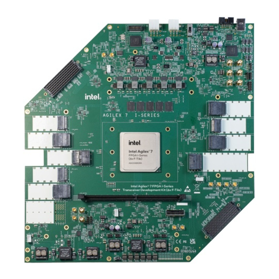
- Page 1 ® Intel Agilex 7 FPGA I-Series Transceiver (6 × F-Tile) Development Kit User Guide 776646 Online Version Send Feedback 2023.05.31...
-
Page 2: Table Of Contents
3.1. Default Settings....................9 3.2. Power Up......................10 3.3. Perform Board Restore..................10 3.3.1. Restore board System Intel MAX 10 with default factory image...... 10 3.3.2. Restore Board QSPI Flash with the Default Factory Image......10 4. Board Test System......................11 4.1. Set Up BTS GUI Running Environment..............11 4.1.1. - Page 3 A.8. Daughter Cards....................52 B. Additional Information....................53 B.1. Safety and Regulatory Information.................53 B.1.1. Safety Warnings..................54 B.1.2. Safety Cautions..................55 B.2. Compliance Information..................58 ® Intel Agilex 7 FPGA I-Series Transceiver (6 × F-Tile) Development Kit User Send Feedback Guide...
-
Page 4: Overview
Intel's standard warranty, but reserves the right to make changes to any 9001:2015 products and services at any time without notice. Intel assumes no responsibility or liability arising out of the Registered application or use of any information, product, or service described herein except as expressly agreed to in writing by Intel. -
Page 5: Feature Summary
1. Overview 776646 | 2023.05.31 1.2. Feature Summary • Intel Agilex 7 I-Series FPGA, 2.7M LE, 3948B package • F-Tile 1 (12A): — 16 FGT transceiver channels fan out to FMC+ connector • F-Tile 2 (12B): — 4 FHT transceiver channels fan out to Quad Small Form Factor Double Density 800 connector (QSFPDD800) —... -
Page 6: Box Contents
1. Overview 776646 | 2023.05.31 1.3. Box Contents • Intel Agilex 7 FPGA I-Series Transceiver Development Kit • Single-rank DDR4 DIMM module • QSPI flash daughter card • USB2.0 Type B cable • 1 × 240 W power adapter and NA/EU/JP/UK cords 1.4. -
Page 7: Getting Started
Intel's standard warranty, but reserves the right to make changes to any 9001:2015 products and services at any time without notice. Intel assumes no responsibility or liability arising out of the Registered application or use of any information, product, or service described herein except as expressly agreed to in writing by Intel. -
Page 8: Design Examples
Contains the development kit documentation – quick start guides and user guide documents Contains: examples • The original data programmed into flash and system Intel MAX 10 before shipment. Use this data to restore the board with its original factory contents. • QSPI image, systemIntel MAX 10 image •... -
Page 9: Power Up The Development Kit
Intel's standard warranty, but reserves the right to make changes to any 9001:2015 products and services at any time without notice. Intel assumes no responsibility or liability arising out of the Registered application or use of any information, product, or service described herein except as expressly agreed to in writing by Intel. -
Page 10: Power Up
This development kit ships with GPIO design examples stored in the QSPI flash device and system Intel MAX 10 pre-programmed. You must perform board restore by using the restore menu under BTS GUI, or using the following instructions through the Intel Quartus Prime Programmer GUI. -
Page 11: Board Test System
Intel's standard warranty, but reserves the right to make changes to any 9001:2015 products and services at any time without notice. Intel assumes no responsibility or liability arising out of the Registered application or use of any information, product, or service described herein except as expressly agreed to in writing by Intel. -
Page 12: Download Openjdk
4. For the Linux system, download the JavaFX Linux x64 SDK. 4.1.3. Install OpenJDK and OpenJFX You have two downloaded zip files, follow these steps to install them. 1. On Windows system, Intel recommends you to unzip the files and put them in the following directory: •... -
Page 13: Run Bts Gui
II JTAG Debug Module and the Signal Tap Logic Analyzer. Intel recommends closing other applications before using BTS, as the GUI is designed based on the Intel Quartus Prime software. The BTS relies on the Intel Quartus Prime software's specific library. Before running the BTS, open the Intel Quartus Prime software to automatically set the environment variable QUARTUS_ROOTDIR. -
Page 14: Test The Functionality Of The Development Kit
4.2. Test the Functionality of the Development Kit This section describes each control in the BTS. 4.2.1. The Bottom Info Bar The bottom information bar shows the status of the system connection, the Intel Quartus Prime version and the JTAG clock. •... -
Page 15: The Sys Info Tab
3. When configuration is completed, the design begins running in the FPGA. The corresponding GUI application tabs that interface with the design is now enabled. If you use the Intel Quartus Prime Programmer for configuration, instead of the BTS GUI, you might need to restart the GUI. -
Page 16: The Gpio Tab
JTAG Chain The JTAG chain control shows all the devices currently in the JTAG chain. Note: You should place the system Intel MAX 10 and FPGA in the JTAG chain when running the BTS GUI. 4.2.4. The GPIO Tab The GPIO tab allows you to interact with all the general-purpose user I/O components on your board. -
Page 17: The Xcvr Tab
The QSFPDD-23 NRZ Tab The following sections describe controls in the QSFPDD NRZ tab. Status The Status control displays the following status information during the loopback test: ® Intel Agilex 7 FPGA I-Series Transceiver (6 × F-Tile) Development Kit User Send Feedback Guide... - Page 18 — Pre-tap 2: Specifies the amount of pre-emphasis on the second pre-tap of the transmitter buffer. — Post-tap 1: Specifies the amount of pre-emphasis on the post-tap of the transmitter buffer. ® Intel Agilex 7 FPGA I-Series Transceiver (6 × F-Tile) Development Kit User Send Feedback Guide...
- Page 19 • Start: This control initiates the loopback tests. • Data Rate: Displays the XCVR type and data rate of each channel. ® Intel Agilex 7 FPGA I-Series Transceiver (6 × F-Tile) Development Kit User Send Feedback Guide...
- Page 20 4.2.5.3. The FMCB NRZ Tab Similar control functions with the QSFPDD NRZ tab except for the port selection. Figure 15. The FMCB NRZ Tab ® Intel Agilex 7 FPGA I-Series Transceiver (6 × F-Tile) Development Kit User Send Feedback Guide...
- Page 21 Similar control functions with the QSFPDD NRZ tab except for the port selection. Figure 17. The QSFP NRZ Tab 4.2.5.6. The SFP Tab Similar control functions with the QSFPDD NRZ tab. ® Intel Agilex 7 FPGA I-Series Transceiver (6 × F-Tile) Development Kit User Send Feedback Guide...
-
Page 22: The Memory Tab
4.2.6. The Memory Tab This tab allows you to read and write DDR4-COMP and DDR4-RDIMM memory on your board. Download the design through BTS Configure. ® Intel Agilex 7 FPGA I-Series Transceiver (6 × F-Tile) Development Kit User Send Feedback Guide... - Page 23 • Test Mode: Infinite Read and Write (default), Single Read and Write. • Test Pattern: PRBS (default), User Defined Constant, Walking ‘0’, Walking ‘1'. ® Intel Agilex 7 FPGA I-Series Transceiver (6 × F-Tile) Development Kit User Send Feedback Guide...
-
Page 24: Control On-Board Clock Through Clock Controller Gui
13. You can also start it using the BTS GUI icon “Clock”. The clock controller communicates with the system Intel MAX 10 device through a 10- pin JTAG header J11 or USB port J10. Then, system Intel MAX 10 controls these programmable clock parts through a 2-wire I C bus. - Page 25 Sets the programmable oscillator frequency for the selected clock to the value in the output controls for Si5391. Frequency changes might take several milliseconds OUTx to take effect. You might see glitches on the clock during this time. Intel recommends resetting the FPGA logic after changing frequencies. Import Si5391 has a two-time rewritable non-volatile memory (NVM).
- Page 26 4. Board Test System 776646 | 2023.05.31 Figure 23. Si5395-1 Similar control functions with Si5391. Figure 24. Si5395-2 Same with Si5395-1. ® Intel Agilex 7 FPGA I-Series Transceiver (6 × F-Tile) Development Kit User Send Feedback Guide...
-
Page 27: Monitor On-Board Power Regulator Through Power Monitor Gui
PCB. The Power Monitor GUI communicates with System Intel MAX 10 through a 10-pin JTAG header J11 or USB port J10. System Intel MAX 10 monitors and controls power regulator, temperature/voltage/current sensing chips through a 2-wire I C bus. - Page 28 When the box is checked, the telemetry data of the selected power rail can be recorded. It saves the data into a .csv file in the directory. Figure 27. Power Monitor GUI—The Temperature Tab ® Intel Agilex 7 FPGA I-Series Transceiver (6 × F-Tile) Development Kit User Send Feedback Guide...
-
Page 29: Identify Test Pass Or Fail-Based On Bts Gui Test Status
Plug four SFP loopback modules in J77 before you configure SFP NRZ example build through BTS GUI. DDR4 DIMM Plug the DIMM module which is shipped alone with this development kit in J5. ® Intel Agilex 7 FPGA I-Series Transceiver (6 × F-Tile) Development Kit User Send Feedback Guide... -
Page 30: Development Kit Hardware And Configuration
Intel's standard warranty, but reserves the right to make changes to any 9001:2015 products and services at any time without notice. Intel assumes no responsibility or liability arising out of the Registered application or use of any information, product, or service described herein except as expressly agreed to in writing by Intel. -
Page 31: Custom Projects For The Development Kit
Intel's standard warranty, but reserves the right to make changes to any 9001:2015 products and services at any time without notice. Intel assumes no responsibility or liability arising out of the Registered application or use of any information, product, or service described herein except as expressly agreed to in writing by Intel. -
Page 32: Revision History
Intel's standard warranty, but reserves the right to make changes to any 9001:2015 products and services at any time without notice. Intel assumes no responsibility or liability arising out of the Registered application or use of any information, product, or service described herein except as expressly agreed to in writing by Intel. -
Page 33: Development Kit Components
Intel's standard warranty, but reserves the right to make changes to any 9001:2015 products and services at any time without notice. Intel assumes no responsibility or liability arising out of the Registered application or use of any information, product, or service described herein except as expressly agreed to in writing by Intel. -
Page 34: Board Components
SI5395-1 IN1N CONN SI5395-1 IN1P CONN 10MHz OUT CONN J140 CLOCK I2C CONN PMBUS CONN ToD CONN SI5518 SPI CONN CLOCK I2C CONN continued... ® Intel Agilex 7 FPGA I-Series Transceiver (6 × F-Tile) Development Kit User Send Feedback Guide... -
Page 35: System Management
System Intel MAX 10 acts as system controller. It handles FPGA AvST configuration, I2C bus access, fan speed control and system reset functions. The UB2/PWR Intel MAX 10 acts as Power manager and on-board JTAG controller. Refer to below description for each function: •... - Page 36 On: bypass from chain Off: enable in chain Chained HPS with SDM nodes internally. ON/ON/OFF SDM is always enabled in the Mode 2: On-board Intel download circuit act as the only JTAG JTAG chain Master. S19.1 (HPS) Chained HPS with SDM nodes externally.
-
Page 37: Power
2.19A@1.8V FPGA +VCCN_IO_GXF Filter VCCLK_GXF 0.78A@1.8V VCCN_IO_GXF +VCCEHT_UX_GXF_U1X FPGA Filter VCCEHT_UX_GXF_U1x 8.89A@1.8V +VCCEHT_UX_GXF_U2X FPGA Filter VCCEHT_UX_GXF_U3x 8.89A@1.8V +VCCERT1_FHT_GXF_1V0_Ux_G1 FPGA LTC7151S P1V0_FHT_Ux_G1_EN VCCERT1_FHT_GXF_1V0 12.2A@1V 12A/12B/12C/13A/13B/13C ® Intel Agilex 7 FPGA I-Series Transceiver (6 × F-Tile) Development Kit User Send Feedback Guide... -
Page 38: Clocks
UB2/PWR MAX10 also shuts down significant power rails when temperature cross the acceptable range. A.4. Clocks Table 8. Default Clock Frequency Schematic Signal Name Default Frequency (Hz) 125M_F_OSC_CLK1 125M CLK_TOD_10M_DN/DP CLK_1PPS_1V2_FM91 continued... ® Intel Agilex 7 FPGA I-Series Transceiver (6 × F-Tile) Development Kit User Send Feedback Guide... - Page 39 SI5518_XTAL_XA FMCA_ETH_REFCLK_156.25M_DP/DN 156.25M FMCB_ETH_REFCLK_156.25M_DP/DN 156.25M SI5518_OUT2_1PPS_PLL_FB FMCA_CPRI_REFCLK_153.6M_DP/DN 153.6M FMCB_CPRI_REFCLK_153.6M_DP/DN 153.6M FMCA_CPRI_REFCLK_184.32M_DP/DN 184.32M FMCB_CPRI_REFCLK_184.32M_DP/DN 184.32M CLK_TOD_10M_DP/DN 156.25M CLK_1PPS_FM91 CLK_1PPS_OUT_SMA CLK_10M_OUT_SMA CLK_SI5518_FREQ_OUT12_156.25M_DP/DN 156.25M CLK_SI5518_FREQ_OUT14_156.25M_DP/DN 156.25M continued... ® Intel Agilex 7 FPGA I-Series Transceiver (6 × F-Tile) Development Kit User Send Feedback Guide...
- Page 40 I2C/SPI REFCLK-2 [GC] REFCLK-1 156.25M-SPARE OUT-3 CTRL/STAT REFCLK-3 [GC] 156.25M REFCLK-2 [GC] 156.25M-SPARE REFCLK-3 [GC] rp_refout REFCLK Intel Agilex 7 FPGA I-Series AGIC040R39A pcie_ep_refin ® Intel Agilex 7 FPGA I-Series Transceiver (6 × F-Tile) Development Kit User Send Feedback Guide...
-
Page 41: General Input/Output
User Switch USER_SW6 User Switch USER_SW7 Reserved GPIO between System Intel MAX 10 and Power Intel MAX 10 SYS_PWR_RSV3 Reserved GPIO between System Intel MAX 10 and Power Intel MAX 10 SYS_PWR_RSV2 Reserved GPIO between System Intel MAX 10 and Power Intel MAX 10... - Page 42 -ST (AVST) configuration SYS_LED0/D9 PGM_LED1 for AVST configuration SYS_LED2/D11 PGM_LED2 for AVST configuration SYS_LED4/D13 MAX_ERROR for AVST configuration SYS_LED6/D15 MAX_LOAD for AVST configuration SYS_LED1/D10 continued... ® Intel Agilex 7 FPGA I-Series Transceiver (6 × F-Tile) Development Kit User Send Feedback Guide...
- Page 43 MUX_DIP_SW2 LOW BEFORE SYSTEM POK HIGH AFTER SYSTEM POK MCIO_CLK_ENN: MUX_DIP_SW3 HIGH BEFORE SYSTEM POK LOW AFTER SYSTEM POK CONNECT VCCL_SCL/SDA TO SYSTEM Intel MAX 10 (DEFAULT ENABLE-1) VCCL_I2C_EN DRIVEN LOW R_13C_PERST_IO_N TIED TO MCIO PREST INTERNALLY R_13B_PERST_IO_N DRIVEN LOW...
- Page 44 DRIVEN LOW R_12A_SPARE_N DRIVEN LOW R_13A_SPARE_N ENABLE ALWAYS AFTER SYSTEM POK DIMM_IO_R_EN LOW BEFORE SYSTEM POK DNU AFTER SYSTEM POK FMC_B_PCIE_PERSTN_3V3 FMC_B_PCIE_WAKEN_3V3 FMC_A_PCIE_WAKEN_3V3 FMC_A_PCIE_PERSTN_3V3 ® Intel Agilex 7 FPGA I-Series Transceiver (6 × F-Tile) Development Kit User Send Feedback Guide...
-
Page 45: Memory Interfaces
A.7. Communication Interfaces MCIO Port (J37) The MCIO slot is a PCIe Gen4 x4 port which fans out from Intel Agilex 7 I-Series FPGA F-tile. This port is designed to meet the standard MCIO pinout. System Intel MAX 10 acts as the board management controller (BMC) of the development kit. - Page 46 QSFPDD2_MODPRS_L Module reset QSFPDD2_RESET_L Mode select QSFPDD2_MODSEL_L Initial mode QSFPDD2_LPMODE Interrupt QSFPDD2_INT_L C clock I2C_QSFP_2_SCL C data I2C_QSFP_2_SDA Transceiver TX QSFPDD2_TX_[0:7]_DP/DN Transceiver RX QSFPDD2_RX_[0:7]_DP/DN ® Intel Agilex 7 FPGA I-Series Transceiver (6 × F-Tile) Development Kit User Send Feedback Guide...
- Page 47 Transceiver RX QSFPDD800_RX_[0:7]_DP/DN QSFP Intel Agilex 7 I-Series development kit supports 3x QSFP ports. QSFP port fans out from the Intel Agilex 7 I-Series FPGA F-tile (FGT). All 4 channels can run up to 1 Gbps per lane. ® Intel Agilex 7 FPGA I-Series Transceiver (6 ×...
- Page 48 Module reset QSFP2_RST Mode select QSFP2_MOD_SEL_L Initial mode QSFP2_LP_MODE Interrupt QSFP2_INTERRUPT_N C clock I2C_QSFP_2_SCL C data I2C_QSFP_2_SDA Transceiver TX QSFP2_TX_[0:3]_DP/DN Transceiver RX QSFP2_RX_[0:3]_DP/DN OSFP ® Intel Agilex 7 FPGA I-Series Transceiver (6 × F-Tile) Development Kit User Send Feedback Guide...
- Page 49 Intel Agilex 7 I-Series development kit supports OSFP ports. OSFP port fans out from the Intel Agilex 7 I-Series FPGA F-tile (FHT). The FHT Tile from bank 13B and 13C can run up to 400 Gbps (50 G x 8) PAM4 in DK-SI-AGI040FES. 4 FHT lanes from bank 13B + 4 FHT lanes from bank 13C are terminated directly to OSFP connector lanes [0:7] (J45).
- Page 50 ) share the same I2C SDM_IO0/12 VCCL_SDA/SCL bus which talks with Intel Agilex 7 FPGA core regulators. By default, SDM acts as SmartVID master and system Intel MAX 10 act as Power GUI master in this chain. System Intel MAX 10 I/Os (...
- Page 51 776646 | 2023.05.31 Intel Agilex 7/System Intel MAX 10 also manages QSFPDD800, 4x QSFPDD, 1DPC DIMM, 3x QSFP, SFP, OSFP, 2x FMC, MCIO I2C buses System Intel MAX 10 supports as a I2C Master for Current ( ) and Temperature sensors...
-
Page 52: Daughter Cards
256MB QSPI flash daughter card This daughter card is pre-programmed with GPIO for AS configuration. It can be re- programmed by customer image. The part number is MT25QU02GCBB8E12-0SIT. ® Intel Agilex 7 FPGA I-Series Transceiver (6 × F-Tile) Development Kit User Send Feedback Guide... -
Page 53: Additional Information
Intel's standard warranty, but reserves the right to make changes to any 9001:2015 products and services at any time without notice. Intel assumes no responsibility or liability arising out of the Registered application or use of any information, product, or service described herein except as expressly agreed to in writing by Intel. -
Page 54: Safety Warnings
To avoid shock, you must ensure that the power cord is connected to a properly wired and grounded receptacle. Ensure that any equipment to which this product is attached to is also connected to properly wired and grounded receptacles. ® Intel Agilex 7 FPGA I-Series Transceiver (6 × F-Tile) Development Kit User Send Feedback Guide... -
Page 55: Safety Cautions
Certain components such as heat sinks, power regulators, and processors may be hot. Heatsink fans are not guarded. Power supply fan may be accessible through guard. Care should be taken to avoid contact with these components. ® Intel Agilex 7 FPGA I-Series Transceiver (6 × F-Tile) Development Kit User Send Feedback Guide... - Page 56 Public Switched Telecommunication Network (PSTN) as it might result in disruption of the network. No formal telecommunication certification to FCC, R&TTE Directive, or other national requirements have been obtained. ® Intel Agilex 7 FPGA I-Series Transceiver (6 × F-Tile) Development Kit User Send Feedback Guide...
- Page 57 Failure to use wrist straps can damage components within the system. Attention: Please return this product to Intel for proper disposition. If it is not returned, refer to local environmental regulations for proper recycling. Do not dispose of this product in unsorted municipal waste.
-
Page 58: Compliance Information
B. Additional Information 776646 | 2023.05.31 Please return this product to Intel for proper disposition. If it is not returned, refer to local environmental regulations for proper recycling. Do not dispose of product in unsorted municipal waste. B.2. Compliance Information...
Need help?
Do you have a question about the Agilex 7 FPGA I-Series and is the answer not in the manual?
Questions and answers