Intel altera Agilex 7 FPGA I Series User Manual
Hide thumbs
Also See for altera Agilex 7 FPGA I Series:
- User manual (71 pages) ,
- User manual (67 pages) ,
- User manual (59 pages)

Related Manuals for Intel altera Agilex 7 FPGA I Series


Summary of Contents for Intel altera Agilex 7 FPGA I Series
- Page 1 Explore more resources ® Altera Design Hub ™ Agilex 7 FPGA I-Series Development Kit User Guide 683288 Online Version Send Feedback 2024.12.20 UG-20338...
-
Page 2: Table Of Contents
2.3. Software and Driver Installation................13 2.3.1. Installing the Quartus Prime Pro Edition Software......... 13 2.3.2. Installing the Development Kit..............14 2.3.3. Installing the Intel FPGA Download Cable II Driver........14 3. Development Kit Setup....................16 3.1. Applying Power to the Development Board.............. 16 3.2. - Page 3 Contents A.6. Network Interfaces....................56 A.7. Port Controller.....................57 A.8. FPGA Configuration....................58 A.9. Supported Configuration Modes................59 A.10. Memory Interfaces..................... 61 A.11. I C........................62 A.12. Clock Circuits....................63 A.13. System Power....................64 A.13.1. Power Guidelines..................65 A.13.2. Power Distribution System...............65 A.13.3. Power Sequence..................67 A.13.4.
-
Page 4: Overview
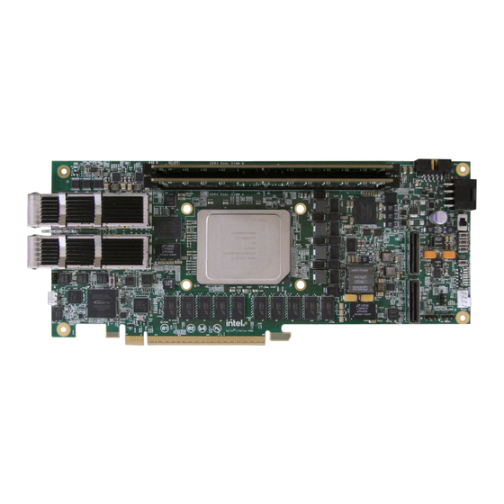
Altera or Intel. Altera and Intel customers are advised to obtain the latest version of device specifications before relying on any published information and before placing orders for products or services. - Page 5 1. Overview 683288 | 2024.12.20 Figure 2. Agilex 7 FPGA I-Series Development Kit (Power Solution 2 Board)—Bottom View Figure 3. Agilex 7 FPGA I-Series Development Kit (Power Solution 1 Board)—Top View ™ Agilex 7 FPGA I-Series Development Kit User Guide Send Feedback...
- Page 6 1. Overview 683288 | 2024.12.20 Figure 4. Agilex 7 FPGA I-Series Development Kit (Power Solution 1 Board)—Bottom View AGIPCIE8000001 Refer to the Appendix A—Development Kit Components section for more details about the components on the Agilex 7 FPGA I-Series Development Kit. Related Information •...
-
Page 7: Block Diagram
This diagram applies to DK-DEV-AGI027RBES, DK-DEV-AGI027-RA, and DK-DEV-AGI027-RA-B. MAX® 10 Config QSPI DIMM2 x72 DIMM x72 Conn FPGA 4 Gb Flash DDR4 DDR4 Intel FPGA JTAG Download Cable II JTAG Header JTAG SW AVST x8 AVST x8 C CTRL I/Os GPIO... - Page 8 This diagram applies to DK-DEV-AGI027RES and DK-DEV-AGI027R1BES. MAX® 10 Comp -CH0 Comp -CH1 FPGA Conn DDR4 x72 with ECC DDR4 x72 with ECC Intel FPGA JTAG Download Cable II JTAG Header JTAG SW AVST x8 Config QSPI C CTRL 2 Gb Flash...
-
Page 9: Feature Summary
— Configuration via Protocol (CvP) configuration support — Storage for two configuration images in flash (factory and user) — JTAG header for device programming ® — Built-in Intel FPGA Download Cable II for device programming • Programmable clock sources — 156.25 MHz differential LVDS for F-Tile (QSFPDD) —... - Page 10 DEV-AGI027-RA: 16 Gb • Communication ports — 2x QSFPDD optical interface port — JTAG header — USB (Micro USB) on-board Intel FPGA Download Cable II — System I2C header • Buttons, switches, and LEDs — System reset push button — CPU reset push button —...
- Page 11 1. Overview 683288 | 2024.12.20 • Mechanical — PCIe standard height form factor (full height, 3/4 length, dual-width) — 4.376" x 10.0" board size — 2 slots height with heatsink • Operating environment — Maximum ambient temperature of 0–35°C • HPS dedicated interfaces (only available on selected board variants, refer to the Agilex 7 FPGA I-Series Development Kit Board Diagram (Power Solution 1 Board) figure)
-
Page 12: Box Contents
1. Overview 683288 | 2024.12.20 1.3. Box Contents • Agilex 7 FPGA I-Series development board • DDR4 DIMM module • USB2.0 Micro-USB cable • 240 W power adapter • NA/EU/JP/UK cords Note: Altera provides only one DIMM module Micron 16GB RDIMM (MTA18ASF2G72PZ-3G2J3) with each development kit. -
Page 13: Getting Started
Altera or Intel. Altera and Intel customers are advised to obtain the latest version of device specifications before relying on any published information and before placing orders for products or services. -
Page 14: Installing The Development Kit
Installation instructions for the Intel FPGA Download Cable II driver for your operating system are available on the Intel website. On the Intel website, navigate to the Cable and Adapter Drivers Information link to locate the table entry for your configuration and click the link to access the instructions. - Page 15 2. Getting Started 683288 | 2024.12.20 Related Information • Cable and Adapter Drivers Information • Intel FPGA Download Cable II User Guide ™ Agilex 7 FPGA I-Series Development Kit User Guide Send Feedback...
-
Page 16: Development Kit Setup
Altera or Intel. Altera and Intel customers are advised to obtain the latest version of device specifications before relying on any published information and before placing orders for products or services. -
Page 17: Default Settings
CORE PMBUS disable CORE PMBUS enable 4: FPGA PMBUS SDM_I2C Bus disable SDM_I2C Bus Enable enable OFF/OFF/OFF/X On-board Intel FPGA Download Cable II is the JTAG host when the SW5[1:4] external JTAG header ( ) is unoccupied. Type continued... ™ Agilex... - Page 18 3. Development Kit Setup 683288 | 2024.12.20 Switch Default Position Function 1: JTAG input source PCIe EP Edge On-Board Intel connector FPGA Download Cable II 2: FPGA Bypass Bypass FPGA FPGA in JTAG chain 3: MAX 10 JTAG MAX 10 JTAG Enable...
- Page 19 CORE PMBUS enable 4: FPGA PMBUS SDM_I2C Bus disable SDM_I2C Bus Enable enable OFF/OFF/OFF/X On-board Intel FPGA Download Cable II is the JTAG host when the SW8[1:4] external JTAG header ( ) is unoccupied. Type 1: JTAG input source PCIe EP Edge...
- Page 20 3. Development Kit Setup 683288 | 2024.12.20 Figure 9. SW2[1:4] Switch Setting Figure 10. SW3[1:4] Switch Setting Figure 11. SW4[1:4] Switch Setting ™ Agilex 7 FPGA I-Series Development Kit User Guide Send Feedback...
- Page 21 QSFPDD_0 connector — QSFPDD_1 connector — USB connector For programming the FPGA using on- board Intel FPGA Download Cable II External JTAG header For use with the external download cable DIMM A connector DDR4 Dual DIMM A DIMM B connector...
-
Page 22: Performing Board Restore Through Quartus Prime Programmer
3. Development Kit Setup 683288 | 2024.12.20 Table 7. LEDs on the Development Kit Board Reference Type Description QSFPDD_0 Link/Activity LED Green LED: User defined QSFPDD_0 Link/Activity LED (Dual • Yellow LED: User defined color) • Green LED: User defined QSFPDD_1 Link/Activity LED Green LED: User defined QSFPDD_1 Link/Activity LED (Dual... -
Page 23: Generating A Pof Image To Program The Flash
3. Development Kit Setup 683288 | 2024.12.20 3.4. Generating a POF Image to Program the Flash Note: If you already have a Programmer Object File ( ), you can skip this section. .pof To generate a POF image to program the flash on the development kit, follow these steps: 1. - Page 24 3. Development Kit Setup 683288 | 2024.12.20 6. Click Configuration Device > Add Device to specify the flash device. In the Device list of the pop-up window, select CFI_2Gb for the configuration flash device. 7. Click on the OPTIONS row, and the click on the Edit option to modify the start address.
-
Page 25: Programming The Generated Pof Image
3. Development Kit Setup 683288 | 2024.12.20 3.5. Programming the Generated POF Image To program the generated POF image, follow these steps: 1. Plug in the USB cable to the USB port (when using , the DIP switch SW5.3 (DK-DEV-AGI027RES and DK-DEV-AGI027R1BES) and (DK-DEV- SW8.3 AGI027RBES and DK-DEV-AGI027-RA) should be off). - Page 26 3. Development Kit Setup 683288 | 2024.12.20 8. Right click the 10M50DAF256 device, Edit > Attach Flash Device, and select Quad SPI Flash Memory QSPI_2Gb. 9. In the Programmer page, click QSPI_2Gb > Change File to select the .pof file. 10.
-
Page 27: The Required Smartvid Qsf Assignments To Compile A Design
3. Development Kit Setup 683288 | 2024.12.20 3.6. The Required SmartVID QSF Assignments to Compile a Design If you are creating your own design and want to generate a programming SRAM object file ( ), you must add the correct SmartVID setting into the Quartus Prime project .sof for the Agilex 7 FPGA I-Series Development Kit to configure successfully. - Page 28 3. Development Kit Setup 683288 | 2024.12.20 Figure 15. Power Management & VID Settings (Power Solution 2 Board) This diagram applies to DK-DEV-AGI027RBES and DK-DEV-AGI027-RA. set_global_assignment -name VID_OPERATION_MODE "PMBUS MASTER" set_global_assignment -name USE_PWRMGT_SCL SDM_IO0 set_global_assignment -name USE_PWRMGT_SDA SDM_IO12 set_global_assignment -name USE_CONF_DONE SDM_IO16 set_global_assignment -name PWRMGT_BUS_SPEED_MODE "100 KHZ"...
- Page 29 3. Development Kit Setup 683288 | 2024.12.20 Figure 16. Power Management & VID Settings (Power Solution 1 Board) This diagram applies to DK-DEV-AGI027RES and DK-DEV-AGI027R1BES. set_global_assignment -name VID_OPERATION_MODE "PMBUS MASTER" set_global_assignment -name USE_PWRMGT_SCL SDM_IO0 set_global_assignment -name USE_PWRMGT_SDA SDM_IO12 set_global_assignment -name USE_CONF_DONE SDM_IO16 set_global_assignment -name PWRMGT_BUS_SPEED_MODE "100 KHZ"...
-
Page 30: Board Test System
Altera or Intel. Altera and Intel customers are advised to obtain the latest version of device specifications before relying on any published information and before placing orders for products or services. -
Page 31: Set Up The Bts Gui Running Environment
4. Board Test System 683288 | 2024.12.20 Figure 18. BTS GUI (Power Solution 1 Board) This diagram applies to DK-DEV-AGI027RES and DK-DEV-AGI027R1BES. 4.1. Set Up the BTS GUI Running Environment To run BTS GUI, including the Power Monitor and Clock Controller GUI, you must download and install Java runtime including OpenJDK and OpenJFX on your systems and set up the running environment. -
Page 32: Downloading Openjfx
4. Board Test System 683288 | 2024.12.20 4.1.2. Downloading OpenJFX 1. Download the Gluon* OpenJFX. Refer to the related information for the download link. 2. Select JavaFX version 17.0.2. a. For the Windows system, download the JavaFX Windows x64 SDK. b. -
Page 33: Test The Functionality Of The Development Kit
4. Board Test System 683288 | 2024.12.20 Figure 19. BTS Folder You can run the BTS GUI easily with the following scripts. 1. On Windows systems, double click the files to run BTS, Clock Controller, or .bat Power Monitor GUIs. Figure 20. -
Page 34: The Bottom Info Bar
4. Board Test System 683288 | 2024.12.20 4.2.1. The Bottom Info Bar The bottom info bar shows the status of the system connection, Quartus Prime version, and the JTAG clock speed. • System Connected/Disconnected: Shows if the board is connected to the system. -
Page 35: The Sys Info Tab
4. Board Test System 683288 | 2024.12.20 Figure 23. The Configure Menu (Power Solution 1 Board) This diagram applies to DK-DEV-AGI027RES and DK-DEV-AGI027R1BES. To configure the FPGA with a test system design, follow these steps: 1. On the Configure menu, click the Configure command that corresponds to the functionality you wish to test. -
Page 36: The Gpio Tab
4. Board Test System 683288 | 2024.12.20 Figure 24. The Sys Info Tab The following sections describe the controls on the Sys Info tab. Board Information The board information control displays static information about your board. • Board Name: Indicates the official name of the board given by the BTS. •... -
Page 37: Qsys Memory Map
4. Board Test System 683288 | 2024.12.20 Figure 25. The GPIO Tab The following sections describe the controls on the GPIO tab. User LEDs The User LEDs control displays the current state of the user LEDs. Toggle the LED buttons to turn the board LEDs on and off. SPI Access Over MAX10 SPI Access Over MAX10 allows you to read and write the data at the address you specify. - Page 38 4. Board Test System 683288 | 2024.12.20 4.2.5.1. The QSFPDD NRZ Tab Figure 26. The QSFPDD NRZ Tab The following sections describe controls in the QSFPDD NRZ tab. Status The Status control displays the following status information during the loopback test: •...
-
Page 39: Pma Setting
4. Board Test System 683288 | 2024.12.20 PMA Setting PMA allows you to make changes to the PMA parameters that affect the active transceiver interface. The following settings are available for analysis: • Serial Loopback: Displays the signal status between the transmitter and the receiver. -
Page 40: Error Control
4. Board Test System 683288 | 2024.12.20 Error Control This control displays data errors detected during analysis and allows you to insert errors: • Detected Errors: Displays the number of data errors detected in the received bitstream. • Inserted Errors: Displays the number of errors inserted into the transmit datastream. -
Page 41: The Ram Tab
4. Board Test System 683288 | 2024.12.20 4.2.5.2. The QSFPDD PAM4 Tab Figure 29. The QSFPDD PAM4 Tab Similar control functions with the QSFPDD NRZ tab. 4.2.6. The RAM Tab This tab allows you to read and write DDR4-COMP0, DDR4-COMP1, DDR4-RDIMM0, and DDR4-RDIMM1 memory on your board. -
Page 42: Performance Indicators
4. Board Test System 683288 | 2024.12.20 Figure 30. The COMP-0 Tab This diagram applies to DK-DEV-AGI027RBES and DK-DEV-AGI027-RA. The following sections describe controls on this tab. Start Initiates DDR4 memory transaction performance analysis. Stop Terminates transaction performance analysis. Performance Indicators These controls display current transaction performance analysis information collected since you last clicked Start: •... -
Page 43: Test Control
4. Board Test System 683288 | 2024.12.20 Test Control • Test Size: You can choose the size of the memory to test. The available options are 64 KB, 256 KB, 1 MB, 4 MB, 16 MB, 64 MB, 256 MB, 1 GB, 4 GB, and 8 GB (default). - Page 44 4. Board Test System 683288 | 2024.12.20 Figure 32. The RDIMM-0 Tab This diagram applies to DK-DEV-AGI027RBES and DK-DEV-AGI027-RA. Similar control functions to the DDR4- COMP0 tab, the total size is 16 GB. ™ Agilex 7 FPGA I-Series Development Kit User Guide Send Feedback...
-
Page 45: Control On-Board Clock Through Clock Controller Gui
4. Board Test System 683288 | 2024.12.20 Figure 33. The RDIMM-1 Tab This diagram applies to DK-DEV-AGI027RBES and DK-DEV-AGI027-RA. Same as RDIMM0. 4.3. Control On-Board Clock through Clock Controller GUI The Clock Controller GUI can change the on-board Si5391 programmable PLLs to any customized frequency between 100 Hz and 712.5 MHz. -
Page 46: Monitor On-Board Power Through Power Monitor Gui
4. Board Test System 683288 | 2024.12.20 Figure 34. Clock Controller GUI The following sections describe the Clock Controller buttons. Read Reads the current frequency setting for the oscillator associated with the active tab. Default Sets the frequency for the oscillator associated with the active tab back to its default value. -
Page 47: Data Record
4. Board Test System 683288 | 2024.12.20 The Power Monitor GUI communicates with System MAX 10 through either USB port J8 or 10-pin JTAG header J10. The MAX 10 monitors and controls power regulators, and temperature/voltage/current sensing chips through a 2-wire I C bus. -
Page 48: Bts Test Areas
4. Board Test System 683288 | 2024.12.20 4.5. BTS Test Areas BTS checks for hardware faults before you can use the board. If one or more BTS test items fail, it implies either a wrong hardware setting or hardware fault on specific interface. -
Page 49: Document Revision History For The Agilex 7 Fpga I-Series Development Kit User Guide
Altera or Intel. Altera and Intel customers are advised to obtain the latest version of device specifications before relying on any published information and before placing orders for products or services. - Page 50 Updated the description for DDR4 DIMMs and QSFPDD0/QSFPDD1 in Identify Test Pass or Fail- based on BTS GUI Test Status section. • Updated Figure: Intel Agilex 7 FPGA I-Series Development Board Image—Front for DK-DEV- AGI027RES and DK-DEV-AGI027R1BES, and DK-DEV-AGI027RBES and DK-DEV-AGI027-RA. •...
- Page 51 Updated development kit name to Intel Agilex 7 FPGA I-Series Development Kit. ® • Retitled the document from Intel Agilex I-Series FPGA Development Kit User Guide to Intel Agilex 7 FPGA I-Series Development Kit User Guide. 2023.02.27 Updated the supported DDR4 speed for memory interfaces in the Feature Summary section.
- Page 52 Updated the PCIe and CXL Interfaces section. • Updated Figure: Intel Agilex I-Series FPGA Development Board Image—Front. • Updated the header of Table: Intel Agilex I-Series FPGA Development Kit Ordering Information. • Updated Table: Factory Default Switch Settings. • Removed the Factory Reset section.
-
Page 53: Development Kit Components
Altera or Intel. Altera and Intel customers are advised to obtain the latest version of device specifications before relying on any published information and before placing orders for products or services. -
Page 54: Agilex 7 Fpga I-Series
A. Development Kit Components 683288 | 2024.12.20 Figure 38. Agilex 7 FPGA I-Series Development Kit (Power Solution 1 Board)—Top View For DK-DEV-AGI027RES and DK-DEV-AGI027R1BES. Figure 39. Agilex 7 FPGA I-Series Development Kit (Power Solution 1 Board)—Bottom View For DK-DEV-AGI027RES and DK-DEV-AGI027R1BES. AGIPCIE8000001 A.2. -
Page 55: Pcie And Cxl Interfaces
A. Development Kit Components 683288 | 2024.12.20 • 3x R-Tile supporting PCIe 5.0 x16 (32Gb/s) or CXL • 1x F tile transceiver supporting 56 Gbps NRZ • Multiple channels to connect to external DDR4 memories A.3. PCIe and CXL Interfaces The Agilex 7 FPGA I-Series Development Kit supports two PCIe/CXL 5.0 x16 interfaces using two out of the FPGA's three R-Tiles, refer to the Block Diagram... -
Page 56: Mcio Cable Assembly Information
A.5. MCIO Cable Assembly Information The cable is not provided with the development kit. For more information, contact Intel Premier Support and quote ID #14016163317. A.6. Network Interfaces The development kit supports two QSFPDD connectors each, connecting to the Agilex 7's F-tile (12A) transceivers. -
Page 57: Port Controller
A. Development Kit Components 683288 | 2024.12.20 aggregator that makes up the Dual 100Gpbs Ethernet interfaces. The FPC202 aggregates all low speed and I C signals across two ports and presents it as a single management interface to the host. The F-Tile (12A) of the FPGA provides 16 general-purpose (FGT) transceiver channels, each 8-channel group is routed to one QSFPDD. -
Page 58: Fpga Configuration
Object File ( .sof FPGA Configuration Setup Ensure the following: • The Quartus Prime Programmer and the Intel FPGA Download Cable II driver are installed on the host computer. • The micro-USB cable is connected to the FPGA development board. •... -
Page 59: Supported Configuration Modes
. The embedded Intel FPGA Download Cable II (or external download cable) or PCIe JTAG can be selected as the source for programming the devices on the chain. The embedded Intel FPGA Download Cable II is the default setting for this configuration mode. - Page 60 MAX 10 Download Cable The on-board Intel FPGA Download Cable II is implemented in a MAX 10 device. A micro-USB connector connects to a CY7C68013A USB2 PHY provides the data to MAX 10. This allows configuration of the FPGA using a USB cable directly connected to a PC running the Quartus Prime software without requiring the external download cable dongle.
-
Page 61: Memory Interfaces
A. Development Kit Components 683288 | 2024.12.20 A.10. Memory Interfaces The following memory information applies to DK-DEV-AGI027-RA-B. • The on-board DDR4 uses five 32 Gb DDR4 single rank devices connecting to Bank 3A, 3B for memory component channel 0 and bank 3C, 3D for memory component channel 1. - Page 62 A. Development Kit Components 683288 | 2024.12.20 • The on-board DDR4 uses five 16 Gb DDR4 single rank devices connecting to Bank 2B, 2E for memory component channel 0 and bank 2C, 2F for memory component channel 1. The total memory size of each channel is 16 GB running at 1200 MHz. •...
-
Page 63: Clock Circuits
A. Development Kit Components 683288 | 2024.12.20 Figure 45. C Chain FPGA_I2C3 I2C3 Level Level Shifter Shifter DDR4 DDR4 DIMM_1 DIMM_2 FPGA_I2C2 I2C2 Level Shifter EEPROM MAX31730 MAX31730 FPC202 TCA9539 M24128 Connector Agilex 7 MAX 10 QSFPDD QSFPDD 1p8_MAIN_I2C FPGA_I2C1 Level Level Shifter... -
Page 64: System Power
A. Development Kit Components 683288 | 2024.12.20 Figure 46. Clock Connection Diagram DDR4_DIMM2, 33.33 MHz, LVDS DDR4_DIMM, 33.33 MHz, LVDS DDR4_comp_ch0, 33.33 MHz, LVDS sys_clk, 100 MHz, LVDS Si5391 Output x12 DDR4_comp_ch1, 33.33 MHz, LVDS osc_clk_1, 125 MHz, LVCMOS Agilex 7 FPGA HPS_OSC_CLK, 25 MHz, LVCMOS 153.6 MHz, LVDS FGTL_refclk_CH0... -
Page 65: Power Guidelines
A. Development Kit Components 683288 | 2024.12.20 A.13.1. Power Guidelines The Agilex 7 FPGA I-Series Development Kit has two modes of operation as described below. In a Standard PCIe-Compliant System In this mode, plug the board into an available PCI Express* slot and connect the standard 2x4 power cords available from the PC's ATX power supply to on the board. - Page 66 A. Development Kit Components 683288 | 2024.12.20 Figure 49. Power Tree Diagram (Power Solution 2 Board) This diagram applies to DK-DEV-AGI027RBES, DK-DEV-AGI027-RA, and DK-DEV-AGI027-RA-B. 12V_GROUP1 12V ATX 2x4 12V_G1 MOSFET MOSFET 12V (DDR4) PWR Conn LTC3888IUHG + LTC7051AV x4 FPGA_VCC U119 + U120, POWER_ON U121, U125,...
-
Page 67: Power Sequence
A. Development Kit Components 683288 | 2024.12.20 Figure 50. Power Tree Diagram (Power Solution 1 Board) This diagram applies to DK-DEV-AGI027RES and DK-DEV-AGI027R1BES. DDR4 4-phase FPGA_VCC_EN ED8401 0.8V VCC (174A) / VCCP (21.34A) +ET6160 x4 U56,U57,U58,U60 0.8V 17.26A VCC_HSSI_GXF_12A (17.26A) VCCL_SDM EM2120L (0.39A) - Page 68 A. Development Kit Components 683288 | 2024.12.20 Figure 51. Power Sequence Power Sequence 12V_PCIe Slot (Grp2) Power In 12V_AUX (Grp1) Power_On 1p2V_PRE 1p8V_PRE Power Ok 3p3V_STBY Group 1 Power On 2p5V_PRE FPGA_VCC/CCP VCCPLLDIG_SDM VCCH/VCCH_SDM VCCL_HPS VCCPLLDIG_HPS VCC_HSSI_GXF VCCERT_FGT_GXF Group1_PG VCCRT_GXR VCC_HSSI_GXR Group 2 Power On VCCED_GXR...
-
Page 69: Power Measurement
A. Development Kit Components 683288 | 2024.12.20 A.13.4. Power Measurement Power measurements are provided for six FPGA power rails by reading the power value of various power regulators via their I C connection. For Power Solution 2 board (DK-DEV-AGI027RBES and DK-DEV-AGI027-RA), the following power rails are monitored: 1. -
Page 70: Mechanical Requirements
A. Development Kit Components 683288 | 2024.12.20 Figure 52. Board Temperature Measurement Circuit 32, 33, 48 CXL_PERSTn 3p3V_STBY 3p3V_STBY 48 FPGA R453 C563 100pf C565 R454 DXP1 fpga_temp0Ap 0.1uF Core A R455 fpga_temp0An DXN1 10.0K C564 100pf R456 temp1_THERMn DXP2 THERM fpga_temp0Cp Core C... -
Page 71: Board Thermal Requirements
A. Development Kit Components 683288 | 2024.12.20 A.16. Board Thermal Requirements A thermal solution is designed to cool up to 250 W total power of the board. An active cooling design is used. The heatsink is designed to meet the height constraints of a 2- slot PCIe card form-factor as defined by the PCIe CEM specification revision 3.0. -
Page 72: Over Temperature Warning Led
A. Development Kit Components 683288 | 2024.12.20 Table 10. Board Operating Conditions Operating Condition Range Maximum power dissipation 250 W Maximum ambient temperature 0°C to 35°C FPGA junction temperature 85°C Related Information Agilex 7 FPGAs and SoCs Device Data Sheet: F-Series and I-Series A.18. -
Page 73: Developer Resources
Altera or Intel. Altera and Intel customers are advised to obtain the latest version of device specifications before relying on any published information and before placing orders for products or services. -
Page 74: Safety And Regulatory Compliance Information
Altera or Intel. Altera and Intel customers are advised to obtain the latest version of device specifications before relying on any published information and before placing orders for products or services. -
Page 75: Safety Warnings
C. Safety and Regulatory Compliance Information 683288 | 2024.12.20 C.1.1. Safety Warnings Power Supply Hazardous Voltage AC mains voltages are present within the power supply assembly. No user serviceable parts are present inside the power supply. Power Connect and Disconnect The AC power supply cord is the primary disconnect device from mains (AC power) and used to remove all DC power from the board/system. -
Page 76: Power Cord Requirements
C. Safety and Regulatory Compliance Information 683288 | 2024.12.20 Power Cord Requirements The plug on the power cord must be a grounding-type male plug designed for use in your region. It must have certification marks showing certification by an agency in your region. -
Page 77: Cooling Requirements
C. Safety and Regulatory Compliance Information 683288 | 2024.12.20 Cooling Requirements Maintain a minimum clearance area of 5 centimeters (2 inches) around the side, front and back of the board for cooling purposes. Do not block power supply ventilation holes and fan. Electro-Magnetic Interference (EMI) This equipment has not been tested for compliance with emission limits of FCC and similar international regulations. -
Page 78: Electrostatic Discharge (Esd) Warning
Failure to use wrist straps can damage components within the system. Attention: Please return this product to Intel for proper disposition. If it is not returned, refer to local environmental regulations for proper recycling. Do not dispose of this product in unsorted municipal waste. -
Page 79: Compliance Information
C. Safety and Regulatory Compliance Information 683288 | 2024.12.20 Please return this product to Intel for proper disposition. If it is not returned, refer to local environmental regulations for proper recycling. Do not dispose of product in unsorted municipal waste.
Need help?
Do you have a question about the altera Agilex 7 FPGA I Series and is the answer not in the manual?
Questions and answers