Advertisement
Quick Links
SERVICE MANUAL
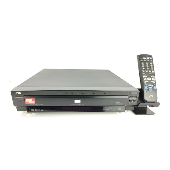
XV-F80BK / XV-F85GD
< ATTENTION ! >
Please pull out the AC plug code after the standby indicator lights pushing the
power supply button without fail after completing the repair.
The mechanism becomes initialed position.
There is a possibility to break when carrying in not initialed position the mechanism
but the state.
Contents
Safety precautions ------------------------ 1-2
Preventing static electricity ------------- 1-3
Importance admistering
point on the safety ------------ 1-4
Precautions for service ----------------- 1-5
DVD VIDEO PLAYER
Each difference point
Model
XV-F80BK
XV-F85GD
Disassembly method -------------------- 1-6
Adjustment method ---------------------- 1-24
Troubleshooting -------------------------- 1-28
Description of major ICs ---------------- 1-32
Glossary of term and abbreviations -- 1-52
This service manual is printed on 100% recycled paper.
COPYRIGHT
2001 VICTOR COMPANY OF JAPAN, LTD.
Body color
Black
Gold
XV-F80BK/XV-F85GD
Area Suffix (XV-F80BK)
J ------------- U.S.A.
C ---------- Canada
Area Suffix (XV-F85GD)
J ------------- U.S.A.
No.A0017
Sep. 2001
Advertisement

Subscribe to Our Youtube Channel
Related Manuals for JVC XV-F80BK


Summary of Contents for JVC XV-F80BK
- Page 1 XV-F80BK/XV-F85GD SERVICE MANUAL DVD VIDEO PLAYER XV-F80BK / XV-F85GD Area Suffix (XV-F80BK) J ------------- U.S.A. C ---------- Canada Area Suffix (XV-F85GD) J ------------- U.S.A. Each difference point Model Body color XV-F80BK Black XV-F85GD Gold < ATTENTION ! > Please pull out the AC plug code after the standby indicator lights pushing the power supply button without fail after completing the repair.
- Page 2 XV-F80BK/XV-F85GD 1. This design of this product contains special hardware and many circuits and components specially for safety purposes. For continued protection, no changes should be made to the original design unless authorized in writing by the manufacturer. Replacement parts must be identical to those used in the original circuits. Services should be performed by qualified personnel only.
- Page 3 XV-F80BK/XV-F85GD Preventing static electricity Electrostatic discharge (ESD), which occurs when static electricity stored in the body, fabric, etc. is discharged, can destroy the laser diode in the traverse unit (optical pickup). Take care to prevent this when performing repairs. 1.1. Grounding to prevent damage by static electricity Static electricity in the work area can destroy the optical pickup (laser diode) in devices such as DVD players.
- Page 4 XV-F80BK/XV-F85GD Importance Admistering point on the Safety CN951 CN952 B320 B103 R956 R952 B316 Q951 Q952 B314 D960 B313 B504 R955 C962 B312 C968 C973 HS952 C970 C978 C969 B310 B502 IC951 B309 C967 C966 C984 C989 L952 C987 L951...
- Page 5 XV-F80BK/XV-F85GD Precautions for Service Handling of Traverse Unit and Laser Pickup 1. Do not touch any peripheral element of the pickup or the actuator. 2. The traverse unit and the pickup are precision devices and therefore must not be subjected to strong shock.
- Page 6 XV-F80BK/XV-F85GD Disassembly method Top cover <Main body> Removing the top cover (See Fig.1) Remove the two screws A on each side of the body. Remove the two screws B on the back of the body. Lift the rear part of the top cover and remove in the direction of the arrow while pulling both sides of the Fig.1...
- Page 7 XV-F80BK/XV-F85GD Removing the main tray assembly Main tray assembly (See Fig.4 to 6) Prior to performing the following procedure, remove the top cover and the front panel assembly. Turn over the body and insert a screwdriver into the slot of the bottom chassis, then move it in the direction of the arrow in Fig.4.
- Page 8 XV-F80BK/XV-F85GD Reattaching the main tray assembly (See Fig.8 to 10) Notch b Main tray assembly Turn over the main tray assembly and pass the card wire extending from the photo sensor board through the notch b, in advance (Fig.8). From above the loading base assembly, turn the...
- Page 9 XV-F80BK/XV-F85GD Loading base assembly Removing the loading base assembly (See Fig.11) Prior to performing the following procedure, remove the top cover, the front panel assembly and the main tray assembly. Servo control board CN210 Disconnect the wire from connector CN808, CN809...
- Page 10 XV-F80BK/XV-F85GD Removing traverse mechanism assembly (See Fig.15 and 16) Clamper base assembly Prior to performing the following procedure, remove Servo control board the top cover and the front panel assembly. CN210 REFERENCE: There is no need to remove the loading base assembly.
- Page 11 XV-F80BK/XV-F85GD Elevator base <Loading base assembly unit> Shafts Prior to performing the following procedures, remove the top cover, the front panel assembly, the main tray assembly, the loading base assembly. Slide gear Removing the elevator base (See Fig.18 and 19)
- Page 12 XV-F80BK/XV-F85GD Removing the belt / load base / slide Loading base assembly gear Prior to performing the following procedures, remove the elevator base. Belt Remove the belt on the upper side of the loading base assembly. Remove the screw R attaching the pulley gear.
- Page 13 XV-F80BK/XV-F85GD Removing the loading motor / loading motor board (See Fig.24 and 25) Remove the two screws U attaching the loading motor on the upper side of the loading base assembly. Turn over the loading base assembly and unsolder the two soldering g on the loading motor board.
- Page 14 XV-F80BK/XV-F85GD Pickup unit <Traverse mechanism unit> Removing the pickup (See Fig.1 to 5) It is not necessary to remove the traverse Flexible board mechanism unit. Solder soldering a on the flexible board next to the pickup unit. From the bottom of the traverse mechanism unit, disconnect the flexible wire from CN101 on the pickup board.
- Page 15 XV-F80BK/XV-F85GD Pickup unit Removing the pickup board (See Fig.1 and 6) It is not necessary to remove the traverse mechanism unit. Flexible board Solder soldering a on the flexible board next to the pickup unit. From the bottom of the traverse mechanism unit, disconnect the flexible wire from CN101 on the pickup board.
- Page 16 XV-F80BK/XV-F85GD Removing the turn table assembly Pickup board (See Fig.6, 8 and 9) Prior to performing the following procedure, remove the traverse mechanism unit. Disconnect the card wire extending from the turn CN101 table assembly, from connector CN201 on the pickup board.
- Page 17 XV-F80BK/XV-F85GD <Main tray assembly unit> Prior to performing the following procedures, remove the top cover, the front panel assembly and the main Main tray assembly tray assembly. Joints a Removing the fitting (See Fig.1) Remove the fitting on the front side of the main tray assembly while releasing the four joints a upward.
- Page 18 XV-F80BK/XV-F85GD Removing the photo sensor board and Sub tray drive motor assembly the sub tray drive motor assembly (See Fig.4) Turn over the main tray assembly and remove the two screws C attaching the photo sensor board. Disconnect the card wire from connector CN082 on CN081 the photo sensor board.
- Page 19 XV-F80BK/XV-F85GD Sub tray position and operation check Sub tray (1) (See Fig.5 and 6) Prior to performing the following procedures, remove the fitting and the main tray cover. CAUTION: Make sure the sub trays are set as shown in Fig.5. When moving the sub trays, put the sub trays which come to the position (4) and (5) forward in turn.
- Page 20 XV-F80BK/XV-F85GD Removing the sub trays (See Fig.8 to 14) Prior to performing the following procedure, remove the main tray cover and the U/D cam (U). CAUTION: Remove the sub tray assembly (4), (3), (2), (5), (6), (7) and (1) in order. When...
- Page 21 XV-F80BK/XV-F85GD Sub tray (4) Reattach the sub tray (3) while inserting the shaft l into the groove m of the main tray, and at the same time, putting the shaft n on the U/D cam (L). Then, Shaft l move the sub tray (3) toward the sub tray (2) until it Sub Tray (3) stops.
- Page 22 XV-F80BK/XV-F85GD Removing the cam switch board assembly (See Fig.15 to 17) Gear cover Prior to performing the following procedure, remove the main tray cover, the U/D cam (U) and the sub trays. Tabs marked p Remove the screw F attaching the gear cover.
- Page 23 XV-F80BK/XV-F85GD Removing the ACT. gear (1), U/D cam (L), cam gear (1) and ACT.gear (2) U/D cam (L) (See Fig.18 and 19) ACT. gear (1) Prior to performing the following procedure, remove the main tray cover, the U/D cam (U) and the sub trays.
- Page 24 XV-F80BK/XV-F85GD Adjustment method (1) Test mode setting method 1)Take out the disc and close the tray. 2)Unplug the power plug. 3)Insert power plug into outlet while pressing both "PLAY" button and "STOP" button of the main body. 4)The player displays "TEST "...
- Page 25 XV-F80BK/XV-F85GD (4) Display of current value of laser 1)Makes to test mode and initializes 2)When "CHOICE" button of remote controller is pushed twice, It is displayed on the FL display, "CHECK". 3)The display of FL display changes from "CHECK" into "LD_ON" if the "TITLE" button of remote controller is pushed.
- Page 26 XV-F80BK/XV-F85GD (6) Upgrading of firmware Please do the up-grade of the firmware after exchanging IC509,IC512,IC513. 1)The power supply is turned on pushing the "POWER" button. 2)The up-grade disk is put on sub-tray 1 pushing OPEN/CLOSE button, and the DISC1 button of the main body is pushed.
- Page 27 XV-F80BK/XV-F85GD Flap adjustment of the pick-up guide shaft <Tool list for adjustment> Stud (four pieces set) Parts No. : JIGXVS40 Hex wrench for adjustment Off-the-shelf (1.3mm) Test disc VT-501 or VT-502 Stud <Adjustment preparation> 1. The metal cover is detached, the OPEN/CLOSE button is pushed, and the tray is done in open.
- Page 28 XV-F80BK/XV-F85GD Troubleshooting Servo volume Press OPEN /CLOSE key Is tray Confirmation of tray drive circuit operation and circuit in surrounding correct? Is the traverse moving See "(3) Traverse movement error" along the innermost in "Check points for individual errors" perimeter for SW detection? "NO DISC"...
- Page 29 XV-F80BK/XV-F85GD Check points for each error (1) Spindle start error 1.Defective spindle motor *Are there several ohms resistance between each pin of CN201 "11-10","10-9","11-9"? (The power supply is turned off and measured.) *Is the sign wave of about 100mVp-p in the voltage had from each terminal? [ CN201"6"(H1-),"7"(H1+),"4"(H2-),"5"(H2+),"2"(H3-),"3"(H3+) ]...
- Page 30 XV-F80BK/XV-F85GD (3) Traverse movement NG 1.Defective traverse driver *Has the voltage come between terminal of CN101 "15" and "13" ? 2.Defective BTL driver (IC271) *Has the motor drive voltage gone out to IC271"17" or "18"? 3.Has the control signal come from servo IC or the microcomputer? *Is it "H"...
- Page 31 XV-F80BK/XV-F85GD (9) Neither picture nor sound is output 1.It is not possible to search *Has the tracking been turned on? *To "(5) Tracking ON NG" in "Check points for each error" when the tracking is not normal. *Is the feed operation normal? To "(3) traverse movement NG"...
- Page 32 XV-F80BK/XV-F85GD Description of major ICs 74LCX373MTC-X(IC512,IC513) 1.Pin layout 2.Pin function 3.Truth table INPUTS OUTPUTS Symbol Description D0~D7 Data inputs Latch enable input Output enable input Q0~Q7 3-State latch outputs H = HIGH Voltage level L = LOW Voltage level Z = High impedance...
- Page 33 XV-F80BK/XV-F85GD AN8702FH(IC101):Frontend processor 1.Pin layout RFINN PC01 RFINP TESTSG PC02 AGCO TGBAL AGCG TBAL PEAK FBAL BOTTOM AN8702FH POFLT RFENV DTRD IDGT OFTR STANDBY DCRF VCC3 STDI RFOUT RSEL RFDIFO JLINE GND3 2.Pin function Symbol Description Symbol Description Pin No.
- Page 34 XV-F80BK/XV-F85GD BA6287F-X(IC451,IC452):Motor driver 1.Pin layout OUT1 OUT2 VREF 2.Block diagram Power save Driver OUT1 Control logic Driver OUT2 Vref 3.Pin function Pin No. Symbol Description Output for motor OUT1 Power supply terminal for drive division Power supply terminal for signal division...
- Page 35 XV-F80BK/XV-F85GD BA6664FM-X(IC251):Spindle motor driver 1.Pin layout 2.Pin function Symbol Description Pin No. Non connect Output 3 for spindle motor Non connect Output 2 for spindle motor Non connect Non connect Output 1 for spindle motor Connect to ground Positive input for hall input AMP 1...
- Page 36 XV-F80BK/XV-F85GD K4S643232E-TC70(IC505):DRAM 1.Block diagram Data input register LDQM Bank select 512K x 32 512K x 32 512K x 32 512K x 32 Column decoder Latency & burst length LCKE Programming register LRAS LCBR LDQM LCAS LWCBR Timing register 2.Pin function...
- Page 37 XV-F80BK/XV-F85GD MN102L25GGW(IC401):Unit CPU Pin function Function Symbol Symbol Function Pin No. Pin No. Micon wait signal input Elevator UP/DOWN switch detect WAIT SWUPDN Read enable SWOPEN Tray OPEN/CLOSE switch detect Spindle muting output to IC251 Serial enable signal for ADSC...
- Page 38 XV-F80BK/XV-F85GD MN103S13BDA(IC301):Optical disc controller 1.Pin layout HDD15 SBCK HDD0 HDD14 HDD1 PVDD HDD13 PVSS HDD2 OSCO1 HDD12 OSCI1 HDD3 LRCK HDD11 BLKCK HDD4 IPFLAG HDD10 DACCLK DACLRCK HDD5 DACDATA HDD9 NTRON MN103S13BDA HDD6 JMPINH HDD8 IDHOLD HDD7 SBCK/PLLOK VDDH CLKOUT2...
- Page 39 XV-F80BK/XV-F85GD 3.Pin function (1/3) Symbol Description Pin No. ATAPI Data HDD15 ATAPI Data HDD0 ATAPI Data HDD14 Power supply 3V ATAPI Data HDD1 ATAPI Data HDD13 ATAPI Data HDD2 Connect to GND ATAPI Data HDD12 Power supply 2.7V ATAPI Data...
- Page 40 XV-F80BK/XV-F85GD 3.Pin function (2/3) Symbol Description Pin No. CPUADR5 System control address CPUADR4 System control address CPUADR3 System control address CPUADR2 System control address CPUADR1 System control address Connect to GND CPUADR0 System control address System control chip select Writing system control...
- Page 41 XV-F80BK/XV-F85GD 3.Pin function (3/3) Symbol Description Pin No. OSCO1 Oscillation output terminal 16.9MHz Power supply 3V PVSS Connect to GND PVDD Power supply 3V Terminal master polarity switch input CIRC-RAM,OVER/UNDER Interruption Connect to GND SBCK Clock output for sub code,serial input...
- Page 42 XV-F80BK/XV-F85GD MN67706ZY (IC201) : Auto digital servo controller 1.Pin layout CHCK40 TSTSG DAT3 DAT2 SYSCLK DAT1 OFTR DAT0 33VDD 33VSS 33VSS 33VDD FBAL TBAL XRESET TGBAL AVSS ROUT CPUIRQ LOUT MN67706ZY CPUCLK AVDD CPUDTIN JLINE CPUDTOUT DBALO MONA VCOF MONB...
- Page 43 XV-F80BK/XV-F85GD 2.Pin function (2/3) Pin No. Symbol Description VFOSHORT VFO short output AVDD Apply 3.3V(For analog circuit) HPFIN Pull-up to VHALF HPFOUT Connect to TP208 AVSS Ground(For analog circuit) LPFIN Pull-up to VHALF LPFOUT Not use CMPIN Connect to TP210...
- Page 44 XV-F80BK/XV-F85GD 2.Pin function (3/3) Pin No. Symbol Description 33VSS Ground(For I/O) 33VDD Apply 3.3V(For I/O) Digital audio interface XRESET Reset input (System control) Servo DSC serial I/F chip select (System control) CIRC serial I/F chip select (System control) CPUIRQ Interrupt request (System control)
- Page 45 XV-F80BK/XV-F85GD NDV8601VWA-BB(IC501):AV Decoder 1.Pin layout 2.Block diagram digital audio Video I/O port audio DAC NTSC Audio MPEG Video Audio digital audio output Video output Video SCART processor decoder processor encoder Serial XBUS serial port controller XBUS peripherals controller RISC SDRAM...
- Page 46 XV-F80BK/XV-F85GD 3.Pin function (NDV8601VWA-BB 2/4) Symbol Description Pin No. Non connect MA11 Connect to ground VSSio 32,33 SDRAM Address bus, reserved for terminal compatibility with 64Mb SDRAM MA12,13 Power supply terminal 1.8V SDRAM Primary bank chip select Power supply terminal 3.3V...
- Page 47 XV-F80BK/XV-F85GD 3.Pin function (NDV8601VWA-BB 3/4) Symbol Description Pin No. Power supply terminal 3.3V VDDio SSP0 Data out or UART0 data-terminal-ready signal SSPOUT0 UART0 Serial data output to an external serial device TXD0 UART0 Serial data input from external serial device...
- Page 48 XV-F80BK/XV-F85GD 3.Pin function (NDV8601VWA-BB 4/4) Symbol Description Pin No. External bus clock used for programmable host peripherals SCLK Programmable WAIT/ACK/RDY control Connect to ground VSSio 163~168 Multiplexed address / data bus terminal AD13~8 Power supply terminal 3.3V VDDio Byte write enable for FLASH,EEPROM,SRAM or peripherals terminal...
- Page 49 XV-F80BK/XV-F85GD NJU3715G-W(IC802) : L.E.D.Driver 1.Pin layout MUTE STLED READY PONLED PROGLED DDPLED ALED DATA 2.Block diagram DATA Latch Shift circuit resistor Control Circuit 3.Pin function Symbol Function PIN No. Parallel conversion data output terminal. D3~D7 Connect to GND. Parallel conversion data output terminal.
- Page 50 XV-F80BK/XV-F85GD SST39VF160-7CEK (IC509) : 16M EEPROM 1. Pin layout /BYTE /RST 2. Block diagram 16,777,216Bit EEPROM X-Decoder Cell Array A19~A0 Address Buffer & Latches Y-Decoder Control Logic I/O Buffers & Data Latches DQ15~DQ0 3. Pin function Symbol Pin name Function...
- Page 51 XV-F80BK/XV-F85GD UPD780232GC-050(IC801):System controller 1.Pin layout 2.Pin function Symbol Description Pin No. Power supply terminal (+5V) VDD1 Connect to ground VSS1 Main system clock oscillation terminal X1,X2 Internal connection (connect to VSS1) IC(VPP) System reset input RESET Serial communications clock input...
- Page 52 XV-F80BK/XV-F85GD Glossary of term and abbreviations (for AV Decoder section) 3-dimension 1)audio/video 2)audio/visual alternating current ACLK audio serial-data (bit) clock multiplexed address / data bus analog-to-digital converter digital audio input address latch enable ANSI/SMPTE American National Standards Institute / Society of Motion Pictures and Television Engineers...
- Page 53 XV-F80BK/XV-F85GD MCLK primary or master clock Megahertz MIPS Million Instructions Per Second MmCPU Mediamatics CPU (synonym for internal RISC CPU) Moving Picture Experts Group Layer-3 Audio (audio file format / extension) MPEG1 audio A digital audio format mainly used in video CDs. It is based on the moving picture expert group (MPEG1) format, a data compression technology.
- Page 54 XV-F80BK/XV-F85GD VICTOR COMPANY OF JAPAN, LIMITED PERSONAL & MOBILE NETWORK BUSINESS UNIT 1644, Shimotsuruma, Yamato, Kanagawa 242-8514, Japan Printed in Japan No.A0017 200109(O)
- Page 55 XV-F80BK/XV-F85GD In regard with component parts appearing on the silk-screen printed side (parts side) of the PWB diagrams, the parts that are printed over with black such as the resistor ( diode ( ) and ICP ( ) or identified by the " " mark nearby are critical for safety.
- Page 56 XV-F80BK/XV-F85GD Block diagrams DVD Servo control & AV decoder section (SHEET 1,2,3,4) (SHEET 2,3,4) AD0~15 PWE0 Flash ROM LADD4~19 LA0~3 ACK FCS IC509 64M SDRAM IC512 IC505 AD4~19 IC513 STD0~7 (Optical disc controller) IC301 BDO OFTR TBAL TE RFENV FBAL...
- Page 57 XV-F80BK/XV-F85GD...
- Page 58 XV-F80BK/XV-F85GD Power supply section (SHEET 6) CN951 CN952 CN953...
- Page 59 XV-F80BK/XV-F85GD Video signal driver section (SHEET 7) TO CN751 AVC DCLK DAC0CS DDATA AOUT0 LRCK MUTE1 SPDIF SHEET 8 L601,L605 IC601 Pr/R/C TO SHEET 5 CVBS/C Pb/B L602 Y/Gr TO CN752 IC602 SHEET 8 C/Cb/B L603 CVBS2/Cr/R L604 AUDIO/VIDEO Signal output section (SHEET 8)
- Page 60 XV-F80BK/XV-F85GD XV-F80BK/XV-F85GD Standard schematic diagrams Frontend & motor driver section TP151 C145 CN101 0.01/16 C107 QGF1012F1-30X K104 NQR0007-002X 0.1/16 C146 K105 R111 NQR0007-002X K106 C104 C115 TP156 NQR0007-002X F1DVD F2DVD TO Pick up unit TESTSG C136 0.047/16 C135 HAGUP R110 0.027/16...
- Page 61 XV-F80BK/XV-F85GD Servo control section D3.3V D2.7V TP158 TP156 TP154 D3.3V -Vdisp C317 1/16 D2.7V Q901 KTC4377 R931 D.GND CN901 QGA2001F2-13X TP131 STD71 R301 TP306 TP132 STD61 R318 C324 R317 0.1/16 R316 R302 TP133 C315 0.1/16 STD51 R303 X301 NAX0375-001X C314 TP134 0.1/16...
- Page 62 XV-F80BK/XV-F85GD XV-F80BK/XV-F85GD AV Decoder section D1.8V D3.3V D3.3V K504 NQR0007-002X C526 C525 C524 C527 TO SHEET 4 22/6.3 00/6.3 R505 AVRTM1 R535 AVRTM R506 STCLK1 R536 STCLK TP917 TP916 R507 STVALID1 R537 STVALID D3.3V R508 STEN1 R538 STEN STD01 R539...
- Page 63 XV-F80BK/XV-F85GD Flash ROM section TO SHEET 3 Flash (IC508,IC509) configuration D3.3V RGB/YC TO SHEET 5 K594 K593 NQR0007-002X NQR0007-002X PAL/NTSC D3.3V LADD16 IC509 CVBS/C SST39VF160 IC512 LADD15 74LCX373MTC-X R517 LADD14 LADD13 C/Cb/B CN551 QGB0807M1-A0 LADD12 AD15 LADD6 LADD10 LADD11 AD10...
- Page 64 XV-F80BK/XV-F85GD XV-F80BK/XV-F85GD FL Display & system control section TO SHEET 7 CN881 DGND RESET TO SHEET 4 -Vdisp R840 CN808 CN8 4 QGA2001C2-06X RF-500TB-12560 D451 EXIN 1SS355-X R847 R835 MUDSW DGND R836 1.5K Q451 QSW0472-001 2SC4081/QR/-X R837 2.2K R453 C809 0.01...
- Page 65 XV-F80BK/XV-F85GD Power supply section T901 QQS0114-001 CP951 D951 C906 Q951 EP951 ERA18-04-T1 ICP-N10-T 0.001/AC250V KTD863/Y/-T R956 QNZ0136-001Z D901 S1WB/A/60-4101 CN951 R952 C960 QGF1016C1-11 C961 C908 R901 82/10 D960 L901 0.0033/1K MTZJ4.7B-T2 QQR1105-001 FC902 C907 C909 R953 ALED FC901 100p/1k D903...
- Page 66 XV-F80BK/XV-F85GD XV-F80BK/XV-F85GD Video signal driver section CN602 DGND QGB1218J2-18X DCLK DAC0CS TO CN751 DDATA AOUTO LRCLK SHEET 8 +12V -12V MUTE1 SPDIF CN603 QGB2510J1-16 DCLK DGND DAC1CS DAC2CS DDATA AOUT2 NOT USE AOUT1 LRCLK MUTE2 MUTE4 D3.3V D.GND TO SHEET 5 C605 100/6.3...
- Page 67 XV-F80BK/XV-F85GD Audio / video signal output section NOT USE CN75 3 QGF1016C1-09 B129 R1187 J756 L1101 R1186 TO CN601 SHEET 7 J755 D1186 1SS133 R1185 D1185 1SS133 DGND R1184 D1184 1SS133 BK761 R1181 J754 R1182 R1183 1SS133 D1183 DGND C1110 0.01GMY...
- Page 68 XV-F80BK/XV-F85GD XV-F80BK/XV-F85GD Printed circuit boards Main board CN951 CN754 B320 B103 CN952 R956 IC754 R952 BK771 B316 Q951 J752 K1162 Q952 R953 B314 D960 C1152 R1163 B313 R1161 C1162 C962 R955 B504 K1161 B312 IC755 C1163 K1163 C968 T1161 B125...
- Page 69 XV-F80BK/XV-F85GD Servo control board Forward side Reverse side C454 TP315 R614 TP413 L202 TP314 TP213 CN807 CN901 Q901 R612 TP316 C622 C616 IC801 IC511 IC505 Q602 IC451 Q603 R855 C573 C237 R856 CN810 R857 C315 C314 R858 TP604 IC501 TP405...
- Page 70 XV-F80BK/XV-F85GD XV-F80BK/XV-F85GD Frontend & motor drive section Reverse side Forward side R275 R289 C161 IC271 R129 R128 R291 C131 R153 R290 C139 C160 TP106 IC101 C138 C277 C126 C144 TP192 C125 C143 R288 TP146 C170 C274 K101 C127 C140 C159...
- Page 71 XV-F80BK/XV-F85GD Operation switch & FL Display board D808 S806 D815 D807 D809 D805 D806 D810 D811 S808 S807 D823 D819 D822 D820 D818 D821 D816 D817 S801 D812 S802 S809 S811 S803 IC804 S810 DI801 D813 S804 CN806 D814 CN814 CN802 Motor &...
-
Page 72: Table Of Contents
XV-F80BK/XV-F85GD PARTS LIST [XV-F80BK/XV-F85GD] * All printed circuit boards and its assemblies are not available as service parts. Area Suffix (XV-F80BK) J ----------- U.S.A. C ----------- Canada Area Suffix (XV-F85GD) J ----------- U.S.A. - Contents - Exploded view of general assembly and parts list ---------- 3-2... -
Page 73: Exploded View Of General Assembly And Parts List
XV-F80BK/XV-F85GD Exploded view of general assembly and parts list Block No. M1MM... - Page 74 METAL COVER QYSBSGY3008E SPECIAL SCREW E406308-003 SPECIAL SCREW 80C,80J E406308-004 SPECIAL SCREW LE20598-001A MECHA FRAME QYSBSG3008Z T.SCREW LE30959-002A STAY BRACKET QYSBSF3008Z SCREW VKZ4001-110S WIRE HOLDER QYSBSG3008Z T.SCREW Explanation of area column 80J =XV-F80BK ver.J 80C =XV-F80BK ver.C 85J =XV-F85GD ver.J...
- Page 75 T.SCREW QQR1267-001 FERRITE CORE LE30966-001A PROTECT SHEET LV10529-001A CHASSIS LV21033-001A TM U/D BASE E65923-003 TAPPING SCREW --------- TRAVERSE MECHANISM See 3-8 page QUQ105-4018AJ FFC WIRE LV41120-003A INSULATOR Explanation of area column 80J =XV-F80BK ver.J 80C =XV-F80BK ver.C 85J =XV-F85GD ver.J...
- Page 76 XV-F80BK/XV-F85GD Parts list (General assembly) Block No. M1MM Item Parts number Parts name Q'ty Description Area LV41120-004A INSULATOR LV41119-001A SPECIAL SCREW LV21035-001A TM U/D CAM E65923-003 TAPPING SCREW QYSBSF3008Z SCREW RF-500TB-12560 MOTOR LV42340-001A MOTOR PULLEY...
-
Page 77: Tray Mechanism Assembly And Parts List
XV-F80BK/XV-F85GD Tray mechanism assembly and parts list Block No. M2MM This FFC wire is the same as the wire "d" in the General assembly(page 3-2). - Page 78 XV-F80BK/XV-F85GD Parts list (Tray mechanism assembly) Block No. M2MM Item Parts number Parts name Q'ty Description Area LV10532-001A MAIN TRAY COVER QYSBSF3008Z SCREW LV21037-001A U/D CAM(U) QYSBSF3008Z SCREW LV10531-001A SUB TRAY LV21036-001A U/D CAM(L) LV32741-001A ACT.GEAR(1) LV10530-001A MAIN TRAY QYSBSF3008Z...
-
Page 79: Traverse Mechanism Assembly And Parts List
XV-F80BK/XV-F85GD Traverse mechanism assembly and parts list Block No. M3MM Grease & Three bond = EBS0006-013B = CFD-4007HYS = 946P = 1401B 65.2 12.0 0.2mm... - Page 80 XV-F80BK/XV-F85GD Parts list (Traverse mechanism assembly) Block No. M3MM Item Parts number Parts name Q'ty Description Area LE20572-001A MECHA BASE LV20635-001A SHAFT HOLDER QYSBST2606M T.SCREW LV31743-002A P.U. SPRING QYSPSGT1416M MINI SCREW QYSBST2606M T.SCREW OPTIMA-2010B1 DVD PICK UP LV31670-001A SWITCH ACTUATOR...
-
Page 81: Grease Points
XV-F80BK/XV-F85GD Grease points Grease = EM-30L-1 = FL-7750 Traverse mechanism UP/DOWN base Both side Traverse mechanism UP/DOWN base 3-10... - Page 82 XV-F80BK/XV-F85GD Grease = EM-30L-1 MAIN TRAY ASSEMBLY APPLY 2 TIMES 3-11...
- Page 83 XV-F80BK/XV-F85GD Grease = EM-30L-1 Load base Traverse mechanism UP/DOWN cam Chassis Apply grease untill bottom of shaft Apply grease on convex surface 3-12...
- Page 84 XV-F80BK/XV-F85GD Grease = EM-30L-1 4 points Apply the bearing of CD roller About 3cm About 2cm 3-13...
- Page 85 XV-F80BK/XV-F85GD Grease = EM-30L-1 = FL-7750 Apply the top surface of rib Back view NOTE : Area, there are not excess grease on surface.(appearance side) Main tray cover 3-14...
- Page 86 XV-F80BK/XV-F85GD Grease = FL-7750 = EM-30L-1 Both side Apply top surface of rib Apply top surface of rib Apply convex part Grease is painted internally in the ditch. Grease is painted internally in the ditch. Main tray Both side 3-15...
- Page 87 XV-F80BK/XV-F85GD Grease = EM-30L-1 = FL-7750 Apply the dent (x5) Action gear (1) (Main tray) 3-16...
- Page 88 XV-F80BK/XV-F85GD Grease = EM-30L-1 UP/DOWN cam (L) 3-17...
- Page 89 XV-F80BK/XV-F85GD Grease = FL-7750 UP/DOWN cam (U) Point of boss Sub tray Point of boss 3-18...
-
Page 90: Electrical Parts List
XV-F80BK/XV-F85GD Electrical parts list (Servo control board) Block No. 01 Item Parts number Parts name Remarks Area Item Parts number Parts name Remarks Area C 201 NCB30JK-474X C CAPACITOR C 407 NCB31CK-104X C CAPACITOR C 204 NCB31HK-331X C CAPACITOR C 408... - Page 91 XV-F80BK/XV-F85GD Electrical parts list (Servo control board) Block No. 01 Item Parts number Parts name Remarks Area Item Parts number Parts name Remarks Area C 582 NEA70JM-226X E CAPACITOR D 614 1SS355-X DIODE C.M C 585 NCB31CK-104X C CAPACITOR D 615 1SS355-X DIODE C.M...
- Page 92 XV-F80BK/XV-F85GD Electrical parts list (Servo control board) Block No. 01 Item Parts number Parts name Remarks Area Item Parts number Parts name Remarks Area R 208 NRSA63J-473X MG RESISTOR R 408 NRSA63J-472X MG RESISTOR R 209 NRSA63J-123X MG RESISTOR R 411...
- Page 93 XV-F80BK/XV-F85GD Electrical parts list (Servo control board) Block No. 01 Item Parts number Parts name Remarks Area R 574 NRSA63J-162X MG RESISTOR R 575 NRSA63J-101X MG RESISTOR R 576 NRSA63J-750X MG RESISTOR R 578 NRSA63J-151X MG RESISTOR R 579 NRSA63J-151X...
- Page 94 XV-F80BK/XV-F85GD Block No. 02 Electrical parts list (Main board) Item Parts number Parts name Remarks Area Item Parts number Parts name Remarks Area BK761 E409182-001SM GRAND TERMINAL C1124 QCZ0202-155Z ML C CAPA I/M 1.5MF C 902 QFZ9067-683 M CAPACITOR C1125...
- Page 95 XV-F80BK/XV-F85GD Electrical parts list (Main board) Block No. 02 Item Parts number Parts name Remarks Area Item Parts number Parts name Remarks Area J 753 QNZ0487-001 OPT TRANSMITTER OPT D.OUT R1116 QRE141J-221Y C RESISTOR 220 5% 1/4W J 754 QNN0434-001...
- Page 96 XV-F80BK/XV-F85GD Electrical parts list (Operation switch & FL Display board) Block No. 03 Item Parts number Parts name Remarks Area Item Parts number Parts name Remarks Area C 806 QER61AM-476Z E CAPACITOR 47MF 20% 10V R 869 NRSA63J-104X MG RESISTOR...
- Page 97 XV-F80BK/XV-F85GD Electrical parts list (Motor & detection switch board) Block No. 04 Item Parts number Parts name Remarks Area C 81 QCZ0202-155Z ML C CAPA I/M 1.5MF C 82 QCZ0202-155Z ML C CAPA I/M 1.5MF C 83 QDVB1EZ-223Y C CAPACITOR...
- Page 98 XV-F80BK/XV-F85GD Electrical parts list (Frontend & Motor driver board) Block No. 06 Item Parts number Parts name Remarks Area Item Parts number Parts name Remarks Area C 101 NCB31CK-104X C CAPACITOR K 101 NQR0007-002X FERRITE BEADS C 105 NEA70JM-476X E.CAPACITOR...
-
Page 99: Packing Materials And Accessories Parts List
XV-F80BK/XV-F85GD Packing materials and accessories parts list Block No. M4MM Block No. M5MM Accessories 3-28... - Page 100 PLUG CORD QAM0328-001 AV CORD 3P RM-SXVF80J REMOCON UNIT 80C,80J RM-SXVF85J REMOCON UNIT A 10 --------- BATTERY A 11 QPC02504015P POLY BAG A 12 BT-52004-2 WARRANTY CARD Explanation of area column 80J =XV-F80BK ver.J 80C =XV-F80BK ver.C 85J =XV-F85GD ver.J 3-29...
Need help?
Do you have a question about the XV-F80BK and is the answer not in the manual?
Questions and answers