Table of Contents
Advertisement
Quick Links
FEATURES
Low power: 1.0 W @ 1 GSPS, 600 mW @ 500 MSPS,
full operating conditions
Single carrier W-CDMA ACLR = 80 dBc @ 80 MHz IF
Analog output: adjustable 8.7 mA to 31.7 mA,
R
= 25 Ω to 50 Ω
L
Novel 2×, 4×, and 8× interpolator/coarse complex modulator
allows carrier placement anywhere in DAC bandwidth
Auxiliary DACs allow control of external VGA and offset control
Multiple chip synchronization interface
High performance, low noise PLL clock multiplier
Digital inverse sinc filter
100-lead, exposed paddle TQFP
APPLICATIONS
Wireless infrastructure
W-CDMA, CDMA2000, TD-SCDMA, WiMax, GSM, LTE
Digital high or low IF synthesis
Internal digital upconversion capability
Transmit diversity
Wideband communications: LMDS/MMDS, point-to-point
COMPLEX I AND Q
FPGA/ASIC/DSP
Rev. B
Information furnished by Analog Devices is believed to be accurate and reliable. However, no
responsibility is assumed by Analog Devices for its use, nor for any infringements of patents or other
rights of third parties that may result from its use. Specifications subject to change without notice. No
license is granted by implication or otherwise under any patent or patent rights of Analog Devices.
Trademarks and registered trademarks are the property of their respective owners.
TYPICAL SIGNAL CHAIN
DC
DIGITAL INTERPOLATION FILTERS
AD9776A/AD9778A/AD9779A
Dual, 12-/14-/16-Bit,1 GSPS
Digital-to-Analog Converters
AD9776A/AD9778A/AD9779A
GENERAL DESCRIPTION
The AD9776A/AD9778A/AD9779A are dual, 12-/14-/16-bit,
high dynamic range digital-to-analog converters (DACs) that
provide a sample rate of 1 GSPS, permitting a multicarrier
generation up to the Nyquist frequency. They include features
optimized for direct conversion transmission applications,
including complex digital modulation and gain and offset
compensation. The DAC outputs are optimized to interface
seamlessly with analog quadrature modulators such as the
ADL537x FMOD series from Analog Devices, Inc. A 3-wire
interface provides for programming/readback of many internal
parameters. Full-scale output current can be programmed over
a range of 10 mA to 30 mA. The devices are manufactured on
an advanced 0.18 μm CMOS process and operate on 1.8 V and
3.3 V supplies for a total power consumption of 1.0 W. They are
enclosed in a 100-lead thin quad flat package (TQFP).
PRODUCT HIGHLIGHTS
1.
Ultralow noise and intermodulation distortion (IMD)
enable high quality synthesis of wideband signals from
baseband to high intermediate frequencies.
2.
A proprietary DAC output switching technique enhances
dynamic performance.
3.
The current outputs are easily configured for various
single-ended or differential circuit topologies.
4.
CMOS data input interface with adjustable setup and hold.
5.
Novel 2×, 4×, and 8× interpolator/coarse complex
modulator allows carrier placement anywhere in DAC
bandwidth.
QUADRATURE
MODULATOR/
MIXER/
AMPLIFIER
DC
I DAC
Q DAC
Figure 1.
One Technology Way, P.O. Box 9106, Norwood, MA 02062-9106, U.S.A.
Tel: 781.329.4700
Fax: 781.461.3113
LO
POST DAC
ANALOG FILTER
A
©2007–2008 Analog Devices, Inc. All rights reserved.
www.analog.com
Advertisement
Table of Contents

Related Manuals for Analog Devices AD9776A


Summary of Contents for Analog Devices AD9776A
-
Page 1: Features
Information furnished by Analog Devices is believed to be accurate and reliable. However, no responsibility is assumed by Analog Devices for its use, nor for any infringements of patents or other One Technology Way, P.O. Box 9106, Norwood, MA 02062-9106, U.S.A. -
Page 2: Table Of Contents
Theory of Operation ..............25 Device Synchronization ..............49 Differences Between AD9776/AD9778/ AD9779 and Synchronization Logic Overview ..........49 AD9776A/AD9778A/AD9779A..........25 Synchronizing Devices to a System Clock ......50 3-Wire Interface ................26 Interrupt Request Operation ............ 50 ... -
Page 3: Revision History
AD9776A/AD9778A/AD9779A REVISION HISTORY 9/08—Rev. A to Rev. B Changes to Auxiliary DAC Operation Section ......44 Replaced Figure 79 ................45 Changed Serial Peripheral Interface (SPI) to 3-Wire Interface Throughout ................... 1 Deleted Figure 79; Renumbered Sequentially ......41 Changes to LO Feedthrough Compensation Section ....45 Change to Features Section .............. -
Page 4: Functional Block Diagram
AD9776A/AD9778A/AD9779A FUNCTIONAL BLOCK DIAGRAM DELAY SYNC_O LINE SYNC_I CLOCK GENERATION/DISTRIBUTION CLOCK REFCLK+ DELAY MULTIPLIER DATACLK LINE 2×/4×/8× REFCLK– DATA ASSEMBLER SINC^-1 OUT1_P 16-BIT I DAC OUT1_N P1D[15:0] LATCH 2× 2× 2× n × n = 0, 1, 2 ... 7... -
Page 5: Specifications
AD9776A/AD9778A/AD9779A SPECIFICATIONS DC SPECIFICATIONS to T , AVDD33 = 3.3 V, DVDD33 = 3.3 V, DVDD18 = 1.8 V, CVDD18 = 1.8 V, I = 20 mA, maximum sample rate, unless OUTFs otherwise noted. Table 1. AD9776A AD9778A AD9779A Parameter... -
Page 6: Digital Specifications
AD9776A/AD9778A/AD9779A DIGITAL SPECIFICATIONS to T , AVDD33 = 3.3 V, DVDD33 = 3.3 V, DVDD18 = 1.8 V, CVDD18 = 1.8 V, I = 20 mA, maximum sample rate, unless OUTFs otherwise noted. LVDS driver and receiver are compliant to the IEEE-1596 reduced range link, unless otherwise noted. -
Page 7: Digital Input Data Timing Specifications
AD9776A/AD9778A/AD9779A DIGITAL INPUT DATA TIMING SPECIFICATIONS All modes, −40°C to +85°C. Table 3. Parameter Conditions Unit INPUT DATA Setup Time Input data to DATACLK Hold Time Input data to DATACLK −0.05 Setup Time Input data to REFCLK −0.80 Hold Time Input data to REFCLK 3.80... -
Page 8: Ac Specifications
AD9776A/AD9778A/AD9779A AC SPECIFICATIONS to T , AVDD33 = 3.3 V, DVDD33 = 3.3 V, DVDD18 = 1.8 V, CVDD18 = 1.8 V, I = 20 mA, maximum sample rate, unless OUTFs otherwise noted. Table 4. AD9776A AD9778A AD9779A Parameter Unit... -
Page 9: Absolute Maximum Ratings
AD9776A/AD9778A/AD9779A ABSOLUTE MAXIMUM RATINGS Table 5. Stresses above those listed under Absolute Maximum Ratings Parameter With Respect To Rating may cause permanent damage to the device. This is a stress AVDD33, DVDD33 AGND, DGND, −0.3 V to +3.6 V rating only; functional operation of the device at these or any... -
Page 10: Pin Configurations And Function Descriptions
NC = NO CONNECT NOTES 1. FOR OPTIMAL THERMAL PERFORMANCE, THE EXPOSED PAD SHOULD BE SOLDERED TO THE GROUND PLANE FOR THE 100-LEAD, THERMALLY ENHANCED TQFP PACKAGE. Figure 3. AD9776A Pin Configuration Table 7. AD9776A Pin Function Descriptions Mnemonic Description Mnemonic Description CVDD18 1.8 V Clock Supply. - Page 11 AD9776A/AD9778A/AD9779A Mnemonic Description Mnemonic Description DVDD18 1.8 V Digital Supply. 3-Wire Interface Port Chip Select Bar. No Connect. RESET Reset, Active High. No Connect. Interrupt Request. No Connect. AGND Analog Ground. DATACLK Data Clock Output. IPTAT Factory Test Pin. Output current is...
- Page 12 AD9776A/AD9778A/AD9779A 100 99 98 97 96 95 94 93 92 91 90 89 88 87 86 85 84 83 82 81 80 79 78 77 76 CVDD18 I120 PIN 1 CVDD18 VREF CGND IPTAT ANALOG DOMAIN CGND AGND REFCLK+ REFCLK–...
- Page 13 AD9776A/AD9778A/AD9779A Mnemonic Description Mnemonic Description DATACLK Data Clock Output. Interrupt Request. DVDD33 3.3 V Digital Supply. AGND Analog Ground. TXENABLE/ Transmit Enable. In single port mode, this IPTAT Factory Test Pin. Output current is IQSELECT pin also functions as IQSELECT.
- Page 14 AD9776A/AD9778A/AD9779A 100 99 98 97 96 95 94 93 92 91 90 89 88 87 86 85 84 83 82 81 80 79 78 77 76 CVDD18 I120 PIN 1 CVDD18 VREF CGND IPTAT ANALOG DOMAIN CGND AGND REFCLK+ REFCLK–...
- Page 15 AD9776A/AD9778A/AD9779A Mnemonic Description Mnemonic Description DATACLK Data Clock Output. Interrupt Request. DVDD33 3.3 V Digital Supply. AGND Analog Ground. TXENABLE/ Transmit Enable. In single port mode, this IPTAT Factory Test Pin. Output current is IQSELECT pin also functions as IQSELECT.
-
Page 16: Typical Performance Characteristics
AD9776A/AD9778A/AD9779A TYPICAL PERFORMANCE CHARACTERISTICS = 160MSPS DATA = 200MSPS DATA –1 –2 = 250MSPS DATA –3 –4 –5 –6 CODE (MHz) Figure 9. AD9779A In-Band SFDR vs. f Figure 6. AD9779A Typical INL 2× Interpolation = 200MSPS = 100MSPS DATA... - Page 17 AD9776A/AD9778A/AD9779A PLL OFF = 160MSPS PLL ON DATA = 200MSPS DATA = 250MSPS DATA (MHz) (MHz) Figure 12. AD9779A Out-of-Band SFDR vs. f Figure 15. AD9779A In-Band SFDR vs. f 2× Interpolation 4× Interpolation, f = 100 MSPS, PLL On/Off...
- Page 18 AD9776A/AD9778A/AD9779A = 160MSPS DATA = 200MSPS DATA = 250MSPS DATA = 75MSPS DATA = 100MSPS DATA = 50MSPS DATA = 125MSPS DATA (MHz) (MHz) Figure 21. AD9779A Third-Order IMD vs. f Figure 18. AD9779A Third-Order IMD vs. f 8× Interpolation 1×...
- Page 19 AD9776A/AD9778A/AD9779A REF 0dBm *ATTEN 20dB *PEAK 10dB EXT REF DC-COUPLED 0dBFS –3dBFS LGAV –6dBFS £(f): FTUN START 1.0MHz STOP 400.0MHz *RES BW 20kHz VBW 20kHz SWEEP 1.203s (601 pts) (MHz) Figure 24. AD9779A IMD Performance vs. f Figure 27. AD9779A Two-Tone Spectrum, Digital Full-Scale Input Over Output Frequency, 4×...
- Page 20 AD9776A/AD9778A/AD9779A –150 –55 –60 –154 –65 0dBFS, PLL ENABLED = 200MSPS –158 –70 = 400MSPS –6dBFS, PLL DISABLED –75 –162 = 800MSPS –80 –166 –85 0dBFS, PLL DISABLED –3dBFS, PLL DISABLED –170 –90 (MHz) (MHz) Figure 30. AD9779A Noise Spectral Density vs. f Figure 33.
- Page 21 AD9776A/AD9778A/AD9779A = 200MSPS DATA = 160MSPS DATA = 250MSPS DATA –0.5 –1.0 –1.5 (MHz) CODE Figure 36. AD9778A Typical INL Figure 39. AD9778A In-Band SFDR vs. f 2× Interpolation –60 –70 FIRST ADJACENT CHANNEL –0.2 THIRD ADJACENT CHANNEL –0.4 –80 –0.6...
- Page 22 = 250MSPS DATA = 200MSPS –0.1 DATA –0.2 –0.3 –0.4 1024 1536 2048 2560 3072 3584 4096 (MHz) CODE Figure 47. AD9776A In-Band SFDR vs. f Figure 44. AD9776A Typical INL 2× Interpolation Rev. B | Page 22 of 56...
- Page 23 CHANNEL –166 –85 –90 –170 (MHz) (MHz) Figure 50. AD9776A Noise Spectral Density vs. f Figure 48. AD9776A ACLR vs. f = 122.88 MSPS, 4× Interpolation, f /4 Modulation Eight-Tone Input with 500 kHz Spacing, f = 200 MSPS DATA DATA REF –25.29dBm...
-
Page 24: Terminology
AD9776A/AD9778A/AD9779A TERMINOLOGY In-Band Spurious-Free Dynamic Range (SFDR) Integral Nonlinearity (INL) INL is defined as the maximum deviation of the actual analog In-band SFDR is the difference, in decibels, between the peak output from the ideal output, determined by a straight line amplitude of the output signal and the peak spurious signal drawn from zero scale to full scale. -
Page 25: Theory Of Operation
AD9779A reads a value of 0x07. The version register of the PLL are wider than those for the AD9776/AD9778/AD9779. AD9776/AD9778/AD9779 reads a value of 0x03. Table 10. Register Value Differences Between AD9776/AD9778/AD9779 and AD9776A/AD9778A/AD9779A PLL Loop Bandwidth, PLL Bias, VCO Control Voltage, PLL VCO Drive, Part No. -
Page 26: 3-Wire Interface
There are two phases of a communication cycle with the device, based on the LSB-first bit (Register 0x00, Bit 6). AD9776A/AD9778A/AD9779A. Phase 1 is the instruction cycle (the writing of an instruction byte into the device), coinciding with Table 12. Byte Transfer Count the first eight SCLK rising edges. -
Page 27: Serial Interface Port Pin Descriptions
AD9776A/AD9778A/AD9779A SERIAL INTERFACE PORT PIN DESCRIPTIONS The serial port controller data address decrements from the data address written toward 0x00 for multibyte I/O operations if the Serial Clock (SCLK) MSB-first format is active. The serial port controller address The serial clock pin synchronizes data to and from the device increments from the data address written toward 0x1F for and controls the internal state machines. -
Page 28: 3-Wire Interface Register Map
AD9776A/AD9778A/AD9779A 3-WIRE INTERFACE REGISTER MAP Note that all unused register bits should be kept at the device default values. Table 13. Address Register Name Decimal Bit 7 Bit 6 Bit 5 Bit 4 Bit 3 Bit 2 Bit 1 Bit 0 Def. - Page 29 AD9776A/AD9778A/AD9779A Table 14. 3-Wire Interface Register Description Register Register Name Address Bits Parameter Function Default Comm 0x00 SDIO bidirectional 0: use SDIO pin as input data only. 1: use SDIO as both input and output data. 0x00 LSB/MSB first 0: first bit of serial data is MSB of data byte.
- Page 30 AD9776A/AD9778A/AD9779A Register Register Name Address Bits Parameter Function Default Sync Control 0x03 DATACLK delay mode 0: manual data timing error detect mode. 1: automatic data timing error detect mode. 0x03 Reserved Should always be set to 1. 0x03 DATACLK Divide[1:0] DATACLK output divider value.
- Page 31 AD9776A/AD9778A/AD9779A Register Register Name Address Bits Parameter Function Default PLL Control 0x08 PLL Band Select[5:0] 111001 This sets the operating frequency range of the VCO. For details (see Table 23). 0x08 PLL VCO Drive[1:0] Controls the signal strength of the VCO output. Set to 11 for optimal performance.
- Page 32 AD9776A/AD9778A/AD9779A Register Register Name Address Bits Parameter Function Default AUX DAC2 Control 0x12 Auxiliary DAC2 Data[9:8] Auxiliary DAC2 Data[9:0] is the 10-bit output current control word. Magnitude of the auxiliary 0x11 Auxiliary DAC2 Data[7:0] 00000000 DAC current increases with increasing value. Bit 9 is the MSB and Bit 0 is the LSB.
-
Page 33: Interpolation Filter Architecture
AD9776A/AD9778A/AD9779A INTERPOLATION FILTER ARCHITECTURE The AD9776A/AD9778A/AD9779A can provide up to 8× inter- Table 16. Low-Pass Filter 2 polation, or the interpolation filters can be entirely disabled. It Lower Coefficient Upper Coefficient Integer Value is important to note that the input signal should be backed off... - Page 34 AD9776A/AD9778A/AD9779A –10 –10 –20 –20 –30 –30 –40 –40 –50 –50 –60 –60 –70 –70 –80 –80 –90 –90 –100 –100 –4 –3 –2 –1 –4 –3 –2 –1 (× Input Data Rate) (× Input Data Rate) Figure 58. 4× Interpolation, Low-Pass Response to ±4× Input Data Rate Figure 61.
- Page 35 –70 the DAC Nyquist bandwidth. –80 The AD9776A/AD9778A/AD9779A are dual DACs with –90 internal complex modulators built into the interpolating filter –100 response. In dual channel mode, the devices expect the real and –4...
- Page 36 AD9776A/AD9778A/AD9779A Table 19. Interpolation Filter Modes, (Register 0x01, Bits[5:2]) Frequency Normalized to f Interpolation Filter Modulation Nyquist Zone Factor[7:6] Mode[5:2] Modulation Pass Band Center High Comments 0x00 −0.05 +0.05 In 8× interpolation; BW (min) = 0.0375 × f 0x01 DC shifted +0.0125...
-
Page 37: Interpolation Filter Bandwidth Limits
AD9776A/AD9778A/AD9779A INTERPOLATION FILTER BANDWIDTH LIMITS The AD9776A/AD9778A/AD9779A use a novel interpolation filter architecture that allows DAC IF frequencies to be gener- –10 ated anywhere in the spectrum. Figure 68 shows the traditional –20 choice of DAC IF output bandwidth placement. Note that there –30... -
Page 38: Inverse Sinc Filter
AD9776A/AD9778A/AD9779A As shown in Table 20, the mixing functions of most of the Table 21. Inverse Sinc Filter modes result in cross-coupling of samples between the I and Q Lower Coefficient Upper Coefficient Integer Value channels. The I and Q channels only operate independently... -
Page 39: Sourcing The Dac Sample Clock
AD9776A/AD9778A/AD9779A SOURCING THE DAC SAMPLE CLOCK The AD9776A/AD9778A/AD9779A offer two modes of sourcing The clock multiplier circuit operates such that the VCO outputs the DAC sample clock (DACCLK). The first mode employs an a frequency, f , equal to the REFCLK input signal frequency on-chip clock multiplier that accepts a reference clock operating multiplied by N1 ×... - Page 40 AD9776A/AD9778A/AD9779A Table 23. Typical VCO Frequency Range vs. PLL Band Select Value PLL Lock Ranges Over Temperature, −40°C to +85°C PLL Lock Ranges Over Temperature, −40°C to +85°C VCO Frequency Range (MHz) VCO Frequency Range (MHz) PLL Band Select PLL Band Select...
- Page 41 AD9776A/AD9778A/AD9779A Configuring PLL Band Select with Temperature Sensing Known Temperature Calibration with Memory The following procedure outlines a method for setting the PLL If temperature sensing is not available in the system, a factory band select value for a device operating at a particular temperature...
-
Page 42: Driving The Refclk Input
AD9776A/AD9778A/AD9779A 0.1µF 50Ω DRIVING THE REFCLK INPUT TTL OR CMOS REFCLK+ CLK INPUT The REFCLK input requires a low jitter differential drive signal. The signal level can range from 400 mV p-p differential to REFCLK– 1.6 V p-p differential centered about a 400 mV input common- 50Ω... -
Page 43: Full-Scale Current Generation
AD9776A/AD9778A/AD9779A FULL-SCALE CURRENT GENERATION INTERNAL REFERENCE AD9776A/AD9778A/AD9779A I DAC GAIN Full-scale current on the I DAC and Q DAC can be set from I DAC 1.2V BAND GAP 8.66 mA to 31.66 mA. Initially, the 1.2 V band gap reference is... -
Page 44: Gain And Offset Correction
AUXILIARY DAC OPERATION be used. A low-pass or band-pass passive filter is recommended Two auxiliary DACs are provided on the AD9776A/AD9778A/ when spurious signals from the DAC (distortion and DAC images) AD9779A. The full-scale output current on these DACs is derived at the quadrature modulator inputs may affect the system perfor- from the 1.2 V band gap reference and external resistor between... -
Page 45: Lo Feedthrough Compensation
DAC. It may –40 take practice before an effective algorithm is achieved. –50 Using the AD9776A/AD9778A/AD9779A evaluation board, the –60 LO feedthrough can typically be adjusted down to the noise floor, although this is not stable over temperature. -
Page 46: Input Data Ports
TXENABLE input is used to power down the digital data path. The simplest method of interfacing to the AD9776A/AD9778A/ AD9779A is when the input data is referenced to the DATACLK In dual port mode, the data must be delivered at the input data output. -
Page 47: Input Data Referenced To Refclk
AD9776A/AD9778A/AD9779A The DATACLKDIV only affects the DATACLK output frequency, SYNC_I not the frequency of the data sampling clock. To maintain an frequency that samples the input data that remains H_SYNC DATACLK consistent with the expected data rate, DATACLKDIV should S_SYNC REFCLK be set to 00. -
Page 48: Optimizing The Data Input Timing
In addition to setting the data timing error IRQ, the data timing error type bit is indicated when an error occurs. The data timing The AD9776A/AD9778A/AD9779A have on-chip circuitry that error type bit is set low to indicate a hold error and high to enables the user to optimize the input data timing by adjusting indicate a setup error. -
Page 49: Device Synchronization
AD9776A/AD9778A/AD9779A DEVICE SYNCHRONIZATION System demands can impose two different requirements for multiple of 32 DACCLK periods. In any case, the maximum synchronization. Some systems require multiple DACs to be frequency of SYNC_I must be less than f DATACLK synchronized to each other. This is the case when supporting Table 30. -
Page 50: Synchronizing Devices To A System Clock
Figure 90 shows the timing of the SYNC_I input with respect to the REFCLK input. Note that although the timing is relative to The AD9776A/AD9778A/AD9779A offer a pulse mode synchro- the REFCLK signal, SYNC_I is sampled at the DACCLK rate. -
Page 51: Power Dissipation
AD9776A/AD9778A/AD9779A POWER DISSIPATION Figure 91 to Figure 99 show the power dissipation of the 1.8 V and 3.3 V digital and clock supplies in single DAC mode and dual DAC mode. In addition to this, the power dissipation/current of the 3.3 V analog supply (mode and speed independent) in single DAC mode is 102 mW/31 mA. -
Page 52: Power-Down And Sleep Modes
AD9776A/AD9778A/AD9779A 0.125 POWER-DOWN AND SLEEP MODES 8× INTERPOLATION, f The AD9776A/AD9778A/AD9779A have a variety of power-down NO MODULATION 0.100 4× INTERPOLATION modes; thus, the digital engine, main TxDACs, or auxiliary DACs can be powered down individually or together. Via the 3-wire interface port, the main TxDACs can be placed in sleep or power- 0.075... -
Page 53: Evaluation Board Overview
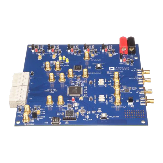
OUTPUT S5 OUTPUT 1 JP15 JP14 AD9779A ADL537x JP16 S6 OUTPUT 2 JP17 LOCAL OSC INPUT S7 DCLKOUT ANALOG DEVICES AD9776A/ AD9778A/ SPI PORT AD9779A Figure 101. AD9776A/AD9778A/AD9779A Evaluation Board Showing All Connections Rev. B | Page 53 of 56... - Page 54 Complete details on the evaluation board and the 3-wire various operating modes. The default software window is interface software can be downloaded from the Analog Devices shown in Figure 102. website.
-
Page 55: Outline Dimensions
AD9776A/AD9778A/AD9779A OUTLINE DIMENSIONS 16.00 BSC SQ 1.20 0.75 0.60 14.00 BSC SQ 0.45 SEATING PIN 1 BOTTOM VIEW PLANE (PINS UP) TOP VIEW (PINS DOWN) CONDUCTIVE HEAT SINK 0.20 1.05 6.50 0.09 1.00 7° 0.95 3.5° FOR PROPER CONNECTION OF 0°... - Page 56 AD9776A/AD9778A/AD9779A NOTES ©2007–2008 Analog Devices, Inc. All rights reserved. Trademarks and registered trademarks are the property of their respective owners. D06452-0-9/08(B) Rev. B | Page 56 of 56...
Need help?
Do you have a question about the AD9776A and is the answer not in the manual?
Questions and answers