Table of Contents
Advertisement
Quick Links
Chipsmall Limited consists of a professional team with an average of over 10 year of expertise in the distribution
of electronic components. Based in Hongkong, we have already established firm and mutual-benefit business
relationships with customers from,Europe,America and south Asia,supplying obsolete and hard-to-find components
to meet their specific needs.
With the principle of "Quality Parts,Customers Priority,Honest Operation,and Considerate Service",our business
mainly focus on the distribution of electronic components. Line cards we deal with include
Microchip,ALPS,ROHM,Xilinx,Pulse,ON,Everlight and Freescale. Main products comprise
IC,Modules,Potentiometer,IC Socket,Relay,Connector.Our parts cover such applications as commercial,industrial,
and automotives areas.
We are looking forward to setting up business relationship with you and hope to provide you with the best service
and solution. Let us make a better world for our industry!
Contact us
Tel: +86-755-8981 8866 Fax: +86-755-8427 6832
Email & Skype: info@chipsmall.com Web: www.chipsmall.com
Address: A1208, Overseas Decoration Building, #122 Zhenhua RD., Futian, Shenzhen, China
Advertisement
Table of Contents

Related Manuals for Xilinx ML623


Summary of Contents for Xilinx ML623
- Page 1 With the principle of “Quality Parts,Customers Priority,Honest Operation,and Considerate Service”,our business mainly focus on the distribution of electronic components. Line cards we deal with include Microchip,ALPS,ROHM,Xilinx,Pulse,ON,Everlight and Freescale. Main products comprise IC,Modules,Potentiometer,IC Socket,Relay,Connector.Our parts cover such applications as commercial,industrial, and automotives areas.
- Page 2 ML623 Virtex-6 FPGA GTX Transceiver Characterization Board User Guide UG724 (v1.1) September 15, 2010...
-
Page 3: Revision History
Xilinx. Xilinx expressly disclaims any liability arising out of your use of the Documentation. Xilinx reserves the right, at its sole discretion, to change the Documentation without notice at any time. Xilinx assumes no obligation to correct any errors contained in the Documentation, or to advise you of any corrections or updates. -
Page 4: Table Of Contents
Online Document ............6 Chapter 1: ML623 Board Features and Operation ML623 Board Features . - Page 5 Appendix A: Default Jumper Positions Appendix B: VITA 57.1 FMC HPC Connector Pinout Appendix C: ML623 Master UCF Listing Appendix D: References www.xilinx.com ML623 Board User Guide UG724 (v1.1) September 15, 2010...
-
Page 6: Preface: About This Guide
Preface About This Guide This document describes the basic setup, features, and operation of the ML623 Virtex-6 FPGA GTX transceiver characterization board. The ML623 board provides the hardware environment for characterizing and evaluating the GTX transceivers available on the Virtex®-6 XC6VLX240T-2FFG1156C FPGA. -
Page 7: Online Document
Blue text in the current document Refer to “Title Formats” in Chapter 1 for details. Go to http://www.xilinx.com Blue, underlined text Hyperlink to a website (URL) for the latest speed files. www.xilinx.com ML623 Board User Guide UG724 (v1.1) September 15, 2010... -
Page 8: Chapter 1: Ml623 Board Features And Operation
Chapter 1 ML623 Board Features and Operation This chapter describes the components, features, and operation of the ML623 Virtex-6 FPGA GTX transceiver characterization board. The ML623 board provides the hardware environment for characterizing and evaluating the GTX transceivers available on the Virtex®-6 XC6VLX240T-2FFG1156C FPGA. -
Page 9: Detailed Description
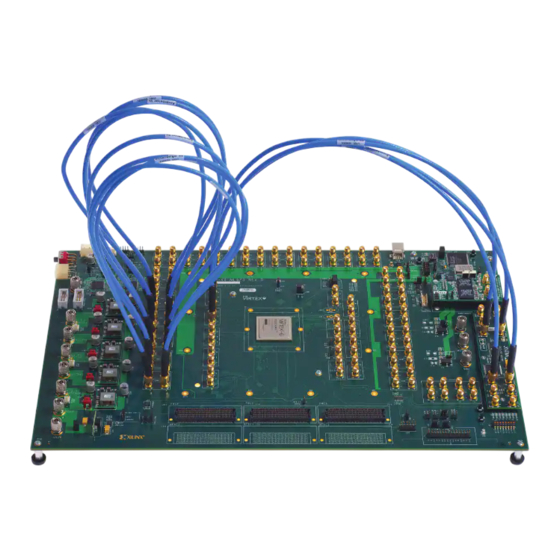
SuperClock-2 Module UG724_c1_01_043010 Figure 1-1: ML623 Board Block Diagram Detailed Description Figure 1-2 shows the ML623 board described in this user guide. Each numbered feature that is referenced in Figure 1-2 is described in the sections that follow. Note: The image in... - Page 10 21c FMC3 connector (J115) Configuration address DIP switch (SW3) System Monitor JTAG isolation jumpers (J22, J23, J195, J196) C Bus Management (U27) UG724_c1_02_063010 Figure 1-2: Detailed Description of ML623 Board Components ML623 Board User Guide www.xilinx.com UG724 (v1.1) September 15, 2010...
-
Page 11: Power Management
Do NOT apply power to J122 and connectors J141 and/or J234 at the same time. Doing so will damage the ML623 board. The ML623 board power is turned on or off by switch SW1. When the switch is in the ON position, power is applied to the board and a green LED (DS36) illuminates. -
Page 12: Onboard Power Regulation
MGTAVTT UG724_c1_03_040810 Figure 1-3: ML623 Board Power Supply Block Diagram The ML623 board uses power regulators and PMBus compliant digital PWM system controllers from Texas Instruments to supply the core and auxiliary voltages listed in Table 1-1. The board can also be configured to use external bench power supply for each voltage. - Page 13 Chapter 1: ML623 Board Features and Operation Table 1-1: Onboard Power System Devices Power External Reference Power Rail Typical Device Description Regulation Supply Designator Net Name Voltage Jumper Jack Core voltage controller and regulators UCD9240PFC PMBus compliant digital PWM system...
-
Page 14: Gtx Transceiver Power Module
PMBus. The PMBus connector, J6, is provided for use with the TI USB Interface Adapter PMBus pod and associated TI GUI. References More information about the power system components used by the ML623 board are available from the Texas Instruments digital power website at: http://www.ti.com/ww/en/analog/digital-power/index.html... -
Page 15: Fpga Configuration
Chapter 1: ML623 Board Features and Operation Technology Module is installed, place jumpers on JP1 and/or JP2 across pins 2–3 (OFF position). Note: The power regulation jumper must be placed in the OFF position before connecting an external supply to its corresponding supply jack. -
Page 16: Prog Push Button
The DONE LED (DS6) indicates the state of the DONE pin of the FPGA. When the DONE pin is High, DS6 lights indicating the FPGA is successfully configured. INIT LED [Figure 1-2, callout 5] The INIT LED (DS20) lights during FPGA initialization. ML623 Board User Guide www.xilinx.com UG724 (v1.1) September 15, 2010... -
Page 17: System Ace Controller
Chapter 1: ML623 Board Features and Operation System ACE Controller [Figure 1-2, callout 6] The onboard System ACE controller (U25) allows storage of multiple configuration files on a CompactFlash card. These configuration files can be used to program the FPGA. The CompactFlash card connects to the CompactFlash card connector (U24) located directly below the System ACE controller on the back side of the board. -
Page 18: 200 Mhz 2.5V Lvds Oscillator
J196 200 MHz 2.5V LVDS Oscillator [Figure 1-2, callout 10] The ML623 board has one 2.5V LVDS differential 200 MHz oscillator (U7) connected to the FPGA global clock inputs. Table 1-5 lists the FPGA pin connections to the LVDS oscillator. -
Page 19: Differential Sma Global Clock Inputs
FPGA I/O by way of 24 control pins, 3 LVDS pairs, 1 regional clock pair, and 1 reset pin. Table 1-8 shows the FPGA I/O mapping for the SuperClock-2 module interface. The ML623 board also supplies 5V, 3.3V, and 2.5V input power to the clock module interface. Table 1-8: SuperClock-2 FPGA I/O Mapping FPGA Pin... -
Page 20: User Leds (Active High)
1-9. These LEDs can be used to indicate status or any other purpose determined by the user. Table 1-9: User LEDs Reference FPGA Pin Net Name Designator LED1 DS17 LED2 DS16 ML623 Board User Guide www.xilinx.com UG724 (v1.1) September 15, 2010... -
Page 21: User Dip Switches (Active High)
Chapter 1: ML623 Board Features and Operation Table 1-9: User LEDs (Cont’d) Reference FPGA Pin Net Name Designator LED3 DS15 LED4 DS14 LED5 DS13 LED6 DS12 LED7 DS11 LED8 DS10 User DIP Switches (Active High) [Figure 1-2, callout 15] The DIP switch SW7 provides a set of eight active-High switches that are connected to user... -
Page 22: User Test I/O
GTX transceivers are grouped into five sets of four (referred to as Quads) which share two differential reference clock pin pairs (Figure 1-7). The transceiver pins and their corresponding SMA connector are shown in Table 1-13. ML623 Board User Guide www.xilinx.com UG724 (v1.1) September 15, 2010... - Page 23 Chapter 1: ML623 Board Features and Operation X-Ref Target - Figure 1-7 QUAD_113 QUAD_114 QUAD_115 116 Clocks 112 Clocks 115 Clocks 113 Clocks 114 Clocks 114 Clocks QUAD_112 QUAD_116 UG724_c1_07_040610 Figure 1-7: GTX Transceiver and Reference Clock SMA Locations Table 1-13: GTX Transceiver Pins...
- Page 24 113_RX3_N 7,175 113_TX3_P 6,595 113_TX3_N 6,599 114_RX0_P 6,112 114_RX0_N 6,119 114_TX0_P 5,441 114_TX0_N 5,449 114_RX1_P 5,096 114_RX1_N 5,102 114_TX1_P 4,435 114_TX1_N 4,442 114_RX2_P J103 4,398 114_RX2_N J100 4,424 114_TX2_P 4,633 ML623 Board User Guide www.xilinx.com UG724 (v1.1) September 15, 2010...
- Page 25 Chapter 1: ML623 Board Features and Operation Table 1-13: GTX Transceiver Pins (Cont’d) FPGA Pin Net Name SMA Connector Trace Length (Mils) 114_TX2_N 4,625 114_RX3_P 5,068 114_RX3_N 5,075 114_TX3_P 5,614 114_TX3_N 5,619 115_RX0_P J136 6,166 115_RX0_N J135 6,172 115_TX0_P J134...
-
Page 26: Gtx Transceiver Clock Input Smas
[Figure 1-2, callout 19] The ML623 board provides differential SMA connectors that can be used for connecting an external function generator to all GTX transceiver reference clock inputs of the FPGA. The FPGA reference clock pins are connected to the SMA connectors as shown in Table 1-14.
Need help?
Do you have a question about the ML623 and is the answer not in the manual?
Questions and answers