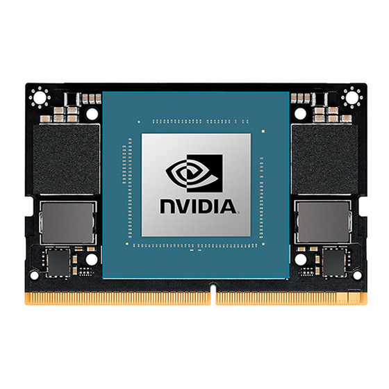

Related Manuals for Nvidia Jetson Orin NX


Summary of Contents for Nvidia Jetson Orin NX
- Page 1 NVIDIA Jetson Orin NX Design Guide DG-10931-001_v0.1 April 2022 PRELIMINARY INFORMATION...
- Page 2 Document History DG-10931-001_v0.1 Version Date Description of Change April 25, 2022 Preliminary information – Subject to change PRELIMINARY INFORMATION NVIDIA Jetson Orin NX DG-10931-001_v0.1 | ii...
-
Page 3: Table Of Contents
Attachments ........................1 Abbreviations and Definitions .................... 2 Chapter 2. Jetson Orin NX ..................3 Chapter 3. Jetson Orin NX Boot Considerations ............. 8 QSPI Boot ..........................8 USB Recovery Mode ......................8 Chapter 4. Developer Kit Feature Considerations ..........9 Button Power MCU ...................... - Page 4 14.1 Unused Multi-Purpose Standard CMOS Pad Interfaces ..........72 14.2 Unused Dedicated Special Purpose Pad Interfaces ............72 Chapter 15. Design and Bring-Up Checklists ............73 Chapter 16. Jetson Orin NX Pin Descriptions ............74 Chapter 17. General Routing Guidelines ..............75 17.1 Signal Naming Convention ....................75 17.2 Routing Guidelines Format ....................
- Page 5 List of Figures Figure 2-1. Jetson Orin NX Block Diagram ................4 Figure 5-1. Jetson Orin NX Module Installed in SODIMM Connector ........12 Figure 5-2. Module to Connector Assembly Diagram ............12 Figure 6-1. System Power and Control Block Diagram ............16 Figure 6-2.
- Page 6 Basic SPI Initiator and Target Connections ............64 Figure 12-4. SPI Topologies ...................... 65 Figure 12-5. Jetson Orin NX UART Connections ..............66 Figure 12-6. Jetson Orin NX CAN Connections ............... 67 Figure 12-7. Jetson Orin NX Fan Connections ................. 68 Figure 12-8.
- Page 7 Jetson Orin NX Power and System Pin Description ........... 13 Table 7-1. Jetson Orin NX USB 2.0 Pin Description ............. 19 Table 7-2. Jetson Orin NX USB 3.2 and PCIe Pin Description ..........20 Table 7-3. USB SS and PCIe Lane Mapping ................. 22 Table 7-4.
- Page 8 CAN Signal Connections ..................68 Table 12-12. Jetson Orin NX Fan Pin Descriptions ..............68 Table 12-13. Jetson Orin NX Debug UART Pin Descriptions ........... 69 Table 12-14. Debug UART Connections ..................69 Table 13-1. Pins Pulled or Driven High by Orin Prior to SYS_RESET* Inactive ....71 Table 13-2.
-
Page 9: Chapter 1. Introduction
Orin (SoC) Technical Reference Manual Jetson Orin NX Module Pinmux Jetson Orin NX Thermal Design Guide Jetson Orin NX SCL (Supported Component List) Attachments The following files are attached to this design guide. Jetson_Orin_NX_Series_Pin_Descriptions.nvxlsx Jetson_Orin_NX_Series_Schematic_Checklist.nvxlsx ... -
Page 10: Abbreviations And Definitions
Power Management Integrated Circuit RJ45 8P8C modular connector used in Ethernet and other data links Real Time Clock Single-Ended Serial Peripheral Interface TMDS Transition-Minimized Differential Signaling UART Universal Asynchronous Receiver-Transmitter Universal Serial Bus PRELIMINARY INFORMATION NVIDIA Jetson Orin NX DG-10931-001_v0.1 | 2... -
Page 11: Chapter 2. Jetson Orin Nx
Chapter 2. Jetson Orin NX The Jetson Orin NX resides at the center of the embedded system solution and includes: Power (Power Sequencer, Regulators, and so on) DRAM (LPDDR5) Gigabit Ethernet Controller QSPI NOR (Boot device) ... -
Page 12: Figure 2-1. Jetson Orin Nx Block Diagram
DIGITAL MIC General Purpose Clocks 2x SPI 2x PWM 3x UART 3x CAN 1x Table 2-2. Jetson Orin NX Connector 260-Pin SO-DIMM Pinout Matrix Module Signal Name Jetson Orin NX Pin # Pin # Module Signal Name Jetson Orin NX Function... - Page 13 USB1_D_P GPIO01 GPIO01 CAM1_PWDN CAM1_PWDN USB2_D_N USB2_D_N CAM1_MCLK CAM1_MCLK USB2_D_P USB2_D_P GPIO02 GPIO02 GPIO03 GPIO03 GPIO04 GPIO04 GPIO05 GPIO05 GPIO06 GPIO06 PCIE0_RX0_N PCIE0_RX0_N PCIE0_RX0_P PCIE0_RX0_P PCIE0_TX0_N PCIE0_TX0_N PCIE0_TX0_P PCIE0_TX0_P PCIE0_RX1_N PCIE0_RX1_N PRELIMINARY INFORMATION NVIDIA Jetson Orin NX DG-10931-001_v0.1 | 5...
- Page 14 I2S1_FS SDMMC_DAT3 PCIE3_CLKREQ* I2S1_SCLK I2S1_SCLK SDMMC_CMD PCIE3_CLK_N GPIO13 GPIO13 SDMMC_CLK PCIE3_CLK_P GPIO14 GPIO14 I2C2_SCL I2C2_SCL SHUTDOWN_REQ* SHUTDOWN_REQ* I2C2_SDA I2C2_SDA PMIC_BBAT PMIC_BBAT UART2_TXD UART2_TXD POWER_EN POWER_EN UART2_RXD UART2_RXD SYS_RESET* SYS_RESET* SLEEP/WAKE* SLEEP/WAKE* PRELIMINARY INFORMATION NVIDIA Jetson Orin NX DG-10931-001_v0.1 | 6...
- Page 15 Module Signal Name Jetson Orin NX Pin # Pin # Module Signal Name Jetson Orin NX Function Function VDD_IN VDD_IN VDD_IN VDD_IN VDD_IN VDD_IN VDD_IN VDD_IN VDD_IN VDD_IN Legend Ground Power Different Functionality PRELIMINARY INFORMATION NVIDIA Jetson Orin NX DG-10931-001_v0.1 | 7...
-
Page 16: Chapter 3. Jetson Orin Nx Boot Considerations
QSPI Boot The Jetson Orin NX module normally boots from QSPI. However, the QSPI’s 64 MB of storage is not expected to contain all the files for a fully functioning system. Secondary storage needs to be provided through NVMe using PCIe. -
Page 17: Chapter 4. Developer Kit Feature Considerations
Jetson Xavier NX Developer Kit carrier board design files are provided as a reference design. Not all the Jetson Orin NX features can be used on the Jetson Xavier NX Developer Kit. In addition, there are some features on the developer kit that are not supported when used with the Jetson Orin NX module. -
Page 18: Usb Superspeed Hub
The ID EEPROM (P3509 - U17) is a feature that is used for NVIDIA internal purposes, but not recommended on a custom design. If a similar functionality is desired for a custom design, avoid using address 7’h57 on the I2C2 interface. -
Page 19: Chapter 5. Modular Connector
Chapter 5. Modular Connector Module Connector Details Jetson Orin NX modules connect to the carrier board using a 260-pin SODIMM connector. The mating connector used on the reference design carrier board will be listed in the Jetson Orin NX SCL (Supported Components List). The connector listed in the Jetson Xavier NX SCL is the same, so that document can be referenced. -
Page 20: Module Installation And Removal
(Envelop view) Standoffs Mounting Screws Module Installation and Removal To install the Jetson Orin NX module correctly, follow the sequence and mounting hardware instructions: Here are some suggested assembly guidelines. Assemble any required thermal solution on the module. Install the module Start with baseboard that has suitable standoff to match SODIMM connector height. -
Page 21: Chapter 6. Power
Jetson Orin NX Data Sheet for supply tolerance and maximum current). CAUTION: Jetson Orin NX is not hot-pluggable. Before installing or removing the module, the main power supply (to VDD_IN pins) must be disconnected and adequate time allowed for the various power rails to fully discharge. -
Page 22: Power Supply And Sequencing
Pull-up voltage on the carrier board on the module ID strap pin is up to the carrier board designer. In the Direction column, Output is from Jetson Orin NX. Input is to Jetson Orin NX. Bidir is for Bidirectional signals. - Page 23 This pull-up will cause the VDD_IN module ID level to be high if a Jetson Orin NX module is installed. The module ID pin should be used on the carrier board to determine if only 5V is supplied to...
-
Page 24: Figure 6-1. System Power And Control Block Diagram
1. MODULE_ID indicates the capability of the module. Low: Legacy module with VDD_IN = 5V nominal. 2. Designs which implement an eFUSE or current limiting device on the input power rail of the module should select a part that DOES NOT limit reverse current. PRELIMINARY INFORMATION NVIDIA Jetson Orin NX DG-10931-001_v0.1 | 16... -
Page 25: Figure 6-3. Power Up Sequence No Power Button - Auto Power On
SHUTDOWN_REQ* Power Button POWER_EN ~14ms SYS_RESET* Notes: 1. SHUTDOWN_REQ* is not driven during power up. The signal is pulled to VDD_IN. 2. SYS_RESET* is driven by the PMIC during power up. PRELIMINARY INFORMATION NVIDIA Jetson Orin NX DG-10931-001_v0.1 | 17... -
Page 26: Figure 6-5. Power Down Initiated By Shutdown_Req* Assertion
VDD_IN 3.0V T > 10mS SHUTDOWN_REQ* POWER_EN Note: SHUTDOWN_REQ* must always be serviced by the carrier board to toggle POWER_EN from high to low, even in cases of sudden power loss. PRELIMINARY INFORMATION NVIDIA Jetson Orin NX DG-10931-001_v0.1 | 18... -
Page 27: Chapter 7. Usb And Pcie
Bidir USB PHY HS_USB0_P2_P USB2_D_P (i.e. M.2 Key E) Note: In the Direction column, Output is from Jetson Orin NX. Input is to Jetson Orin NX. Bidir is for Bidirectional signals. PRELIMINARY INFORMATION NVIDIA Jetson Orin NX DG-10931-001_v0.1 | 19... -
Page 28: Table 7-2. Jetson Orin Nx Usb 3.2 And Pcie Pin Description
USB and PCIe Table 7-2. Jetson Orin NX USB 3.2 and PCIe Pin Description Module Pin Recommended Pin # Name Orin Signal Usage and Description Usage Direction Pin Type HS_UPHY0_L4_RX_ PCIE0_RX0_N PCIe #0 Receive 0 (PCIe Ctrl #4 Lane 0) - Page 29 GP185_PCIE_WAKE PCIe Wake. 47kΩ pull-up to 3.3V on the Shared between Open PCIE_WAKE* Input module. PCIe interfaces. Drain 3.3V HS_UPHY0_L0_RX_ USB SS USBSS_RX_N USB SS Receive (USB 3.2 Port #0) Input PRELIMINARY INFORMATION NVIDIA Jetson Orin NX DG-10931-001_v0.1 | 21...
-
Page 30: Table 7-3. Usb Ss And Pcie Lane Mapping
Notes: In the Direction column, Output is from Jetson Orin NX. Input is to Jetson Orin NX. Bidir is for Bidirectional signals. The direction shown in this table for GPxxx_PCIEx_RST* and GP185_PCIE_WAKE* signals is true when used for those PCIe functions. -
Page 31: Usb
USB and PCIe Jetson Orin NX supports up to three USB 2.0 ports and up to three USB 3.2 ports. Two examples are shown in Figure 7-1 and Figure 7-2. Note: Some non-compliant USB 3.0 devices will not function correctly unless USB 3.2 Gen2 is disabled. -
Page 32: Usb 2.0 Design Guidelines
Resonance Dip Frequency > 8 budget [*] the consideration of Gen1 fixture loss Time-domain Reflectometer (TDR) Dip @ Tr = 200ps (10%-90%) Gen1 Ω @ Tr = 61ps (10%-90%) Gen2 PRELIMINARY INFORMATION NVIDIA Jetson Orin NX DG-10931-001_v0.1 | 24... - Page 33 4 if all vias are PTH via Micro Vias Not limited if total channel loss meets IL spec Max Via Stub Length long via stub requires review (IL and resonance dip check) PRELIMINARY INFORMATION NVIDIA Jetson Orin NX DG-10931-001_v0.1 | 25...
- Page 34 GND plane under signal pad should be voided. Size of void should be the same size as the pad. Connector used must be USB-IF certified General: See Chapter 17 for guidelines related to serpentine routing, routing over voids and noise coupling PRELIMINARY INFORMATION NVIDIA Jetson Orin NX DG-10931-001_v0.1 | 26...
-
Page 35: Figure 7-3. Il/Next Plot
USB and PCIe The following figures show the USB 3.2. Interface signal routing requirements. Figure 7-3. IL/NEXT Plot Figure 7-4. TDR Plot Figure 7-5. Via Topology Figure 7-6. Component Order PRELIMINARY INFORMATION NVIDIA Jetson Orin NX DG-10931-001_v0.1 | 27... -
Page 36: Common Usb Routing Guidelines
(through 100ohm series resistor to OC pin). GPIO (VBUS Detect) 5V to 1.8V level shifter VBUS Detect: Connect to VBUS pin of USB connector receiving USB0_+/– interface through level shifter. PRELIMINARY INFORMATION NVIDIA Jetson Orin NX DG-10931-001_v0.1 | 28... -
Page 37: Pcie
PCIe Jetson Orin NX brings four PCIe interfaces to the module pins for up to seven total lanes (1 x4 + 1 x1 + 1x2) for use on the carrier board. The PCIe x4 interface (PCIE0) operates up to Gen4 speed and supports both Root Port and Endpoint operation. -
Page 38: Figure 7-9. Pcie Root Port Connections Example
3. See design guidelines for correct AC capacitor values. 4. The PCIe REFCLK inputs and CLK outputs comply to the PCIe CEM specification “REFCLK DC Specifications and AC Timing Requirements.” The clocks are HCSL compatible. PRELIMINARY INFORMATION NVIDIA Jetson Orin NX DG-10931-001_v0.1 | 30... -
Page 39: Figure 7-10. Pcie Endpoint Connections Example
3. See design guidelines for correct AC capacitor values. 4. Isolation circuitry is required on the PCIe control signals when Jetson Orin NX is configured as Endpoint. These isolate the lines from the on-module pull-ups as well as ensure the Endpoint and Root Port devices do not have their pads driven high before power is applied. -
Page 40: Pcie Design Guidelines
Insertion loss / length (delay) -10.5 / 310 (1985) Gen 3.0: -6.5 dB @4GHz Routing to PCIe/M.2 connector/module: The PCIe/M.2 connector/card loss Insertion loss / length (delay) -7.6 / 224 (1437) assumption is: PRELIMINARY INFORMATION NVIDIA Jetson Orin NX DG-10931-001_v0.1 | 32... -
Page 41: Figure 7-11. Zig-Zag Routing Example
The max length and delay numbers are examples. These should be updated based on the actual PCB material loss and the loss for the end device and any additional connections. Figure 7-11. Zig-Zag Routing Example PRELIMINARY INFORMATION NVIDIA Jetson Orin NX DG-10931-001_v0.1 | 33... -
Page 42: Figure 7-12. Insertion Loss S-Parameter Plot Sdd21
USB and PCIe Figure 7-12. Insertion Loss S-Parameter Plot SDD21 Figure 7-13. Insertion Loss S-Parameter Plot SDD11 Figure 7-14. AC Cap Voiding Figure 7-15. Connector Voiding PRELIMINARY INFORMATION NVIDIA Jetson Orin NX DG-10931-001_v0.1 | 34... -
Page 43: Table 7-10. Pcie Signal Connections
Differential Receive Data Pair: Connect to RX_N/P pins of PCIe (PCIE2_RX1_N/P) capacitors near Jetson connector or TX_N/P pin of PCIe device through AC cap according CSI4_D2_N/P Xavier NX pins or to supported configuration. (PCIE2_RX0_N/P) device if device on main PCB. PRELIMINARY INFORMATION NVIDIA Jetson Orin NX DG-10931-001_v0.1 | 35... - Page 44 This isolates the on- module pull-up resistors as well as ensures this signal will not be pulled or driven high before the Root Port is powered on. PRELIMINARY INFORMATION NVIDIA Jetson Orin NX DG-10931-001_v0.1 | 36...
-
Page 45: Chapter 8. Gigabit Ethernet
GBE_MDI3_N − GbE Transformer Data 3 GBE_MDI3_P − Notes: In the Direction column, Output is from Jetson Orin NX. Input is to Jetson Orin NX. Bidir is for Bidirectional signals. Figure 8-1. Jetson Orin NX Ethernet Connections Jetson 3.3V UPHY2... -
Page 46: Figure 8-2. Gigabit Ethernet Magnetics And Rj45 Connections
Ideally there should be no vias, but if required for breakout to Ethernet controller or magnetics, keep very close to either device. Notes: NVIDIA Orin does not support delay or skewing of clock vs. data. This must be enabled in the PHY. Table 8-3. Ethernet Signal Connections... -
Page 47: Chapter 9. Display
Notes: In the Direction column, Output is from Jetson Orin NX. Input is to Jetson Orin NX. Bidir is for Bidirectional signals. The direction shown in this table for DP_AUX_CH[1:0]_HPD is true when used for Hot-plug Detect. Otherwise, if used as GPIOs, the direction is bidirectional. -
Page 48: Edp And Dp
LANE_0P Notes: 1. Level shifter required on DP0_HPD to avoid the pin from being driven when Jetson Orin NX is off. The level shifter must be non-inverting (preserve the polarity of the HPD signal from the display). The reference design uses a BJT level shifter, and a resistor divider is needed. See the reference design if a similar approach will be used. -
Page 49: Edp And Dp Routing Guidelines
DP Routing Guidelines The following routing requirements meet the eDP and DP routing guidelines. Figure 9-3. eDP and DP Differential Main Link Topology Jetson Common Mode Chokes & ESD Driver Conn PRELIMINARY INFORMATION NVIDIA Jetson Orin NX DG-10931-001_v0.1 | 41... -
Page 50: Table 9-3. Edp And Dp Main Link Signal Requirements Including Dp_Aux
6.9ps/mm assumption for Stripline, Max trace length (delay) from module to connector 5.9ps/mm for Microstrip. RBR/HBR Stripline 215 (1137.5) mm (ps) Microstrip 215 (975) HBR2 Stripline 184 (1260) Microstrip 178 (1050) HBR3 PRELIMINARY INFORMATION NVIDIA Jetson Orin NX DG-10931-001_v0.1 | 42... - Page 51 No requirement HBR2/HBR3 Voiding HBR2: Voiding the plane directly under the pad ~0.1mm larger than the pad size is RBR/HBR No requirement recommended. HBR2/HBR3 Voiding required Serpentine (See USB 3.2 Guidelines) PRELIMINARY INFORMATION NVIDIA Jetson Orin NX DG-10931-001_v0.1 | 43...
-
Page 52: Figure 9-4. S-Parameter Up To Hbr2
The following figures show the eDP and DP interface signal routing requirements. Figure 9-4. S-Parameter Up to HBR2 Figure 9-5. S-Parameter Up to HBR3 PRELIMINARY INFORMATION NVIDIA Jetson Orin NX DG-10931-001_v0.1 | 44... -
Page 53: Figure 9-6. Via Topology #1
DP1_HPD Level shifter (1.8V on module side, 3.3V on eDP/DP: Hot Plug Detect: Connect to HPD DP/eDP connector side) and ESD to GND.. pin on display connector through level shifter. PRELIMINARY INFORMATION NVIDIA Jetson Orin NX DG-10931-001_v0.1 | 45... -
Page 54: Hdmi
TPD4E 02B04 DQO R Notes: 1. Level shifters required on DDC/HPD. NVIDIA Orin pads are not 5V tolerant and cannot directly meet HDMI VIL/VIH requirements. HPD level shifter can be non-inverting or inverting. The HPD level shifter in the reference design is inverting. The reference design uses a BJT level shifter, and a resistor divider is needed. -
Page 55: Figure 9-9. Hdmi Clk And Data Topology
The max length (delay) is derived based < 0.8 dB/in. @ 3GHz on this characteristic. The length (delay) < 0.4 dB/in. @ 1.5GHz constraint must be re-defined if the loss characteristic is changed. See Note 1. PRELIMINARY INFORMATION NVIDIA Jetson Orin NX DG-10931-001_v0.1 | 47... - Page 56 (seg A) Max distance between ESD and signal via Add-on Components Example of a case where space is limited for Top: See Figure 9-16 Bottom: See Figure 9-17 placing components. PRELIMINARY INFORMATION NVIDIA Jetson Orin NX DG-10931-001_v0.1 | 48...
- Page 57 Trace at Component Region Value Ω ± 10% Location At component region (Microstrip) Trace entering the SMT pad One 45° See Figure 9-22 Trace between components Uncoupled structure See Figure 9-23 HDMI connector PRELIMINARY INFORMATION NVIDIA Jetson Orin NX DG-10931-001_v0.1 | 49...
-
Page 58: Figure 9-10. Il/Fext Plot
Solutions with flex/2nd PCB may not achieve maximum frequency operation. The following figures show the HDMI interface signal routing requirements. Figure 9-10. IL/FEXT Plot Figure 9-11. TDR Plot Figure 9-12. HDMI Via Topology PRELIMINARY INFORMATION NVIDIA Jetson Orin NX DG-10931-001_v0.1 | 50... -
Page 59: Figure 9-13. Connector Pin Via
Connector Pin Via Figure 9-14. Via No Breakout Figure 9-15. Via Breakout on Same Layer as Main Trunk Figure 9-16. Add On Components – Top Figure 9-17. Add On Components – Bottom PRELIMINARY INFORMATION NVIDIA Jetson Orin NX DG-10931-001_v0.1 | 51... -
Page 60: Figure 9-18. Ac Cap Void
Figure 9-18. AC Cap Void Figure 9-19. RPD, Choke, FET Placement Figure 9-20. ESD Footprint Figure 9-21. ESD Void Figure 9-22. SMT Pad Trace Entering Figure 9-23. SMT Pad Trace Between PRELIMINARY INFORMATION NVIDIA Jetson Orin NX DG-10931-001_v0.1 | 52... -
Page 61: Figure 9-24. Connector Voiding
HDMI 5V supply to connector: Connect recommended) on supply near connector and ESD to +5V on HDMI connector. to GND. Note: Any ESD and/or EMI solutions must support targeted modes (frequencies). PRELIMINARY INFORMATION NVIDIA Jetson Orin NX DG-10931-001_v0.1 | 53... -
Page 62: Chapter 10. Mipi Csi Video Input
CSI3_D1_N HS_CSI3_D1_N Camera, CSI 3 Data 1 CSI3_D1_P HS_CSI3_D1_P Notes: In the Direction column, Output is from Jetson Orin NX. Input is to Jetson Orin NX. Bidir is for Bidirectional signals. PRELIMINARY INFORMATION NVIDIA Jetson Orin NX DG-10931-001_v0.1 | 54... -
Page 63: Figure 10-1. Csi Connection Options
Notes: 1. In the Direction column, Output is from Jetson Orin NX. Input is to Jetson Orin NX. Bidir is for Bidirectional signals. 2. The direction shown in this table for CAM[1:0]_MCLK and CAM[1:0]_PWDN is true when used for those functions. These pins are GPIOs and can support input or output (bidirectional). -
Page 64: Csi Design Guidelines
Via proximity (signal to reference) < 0.65 (3.8) mm (ps) Intra-pair trace spacing 0.15mm Can be adjusted to meet Differential Impedance. Trace spacing: Microstrip / Stripline 2x / 2x dielectric Max PCB breakout delay PRELIMINARY INFORMATION NVIDIA Jetson Orin NX DG-10931-001_v0.1 | 56... -
Page 65: Table 10-5. Mipi Csi Signal Connections
CAM[1:0]_MCLK Camera Initiator Clocks: Connect to camera reference clock inputs. GPIO01 (opt. MCLK2) GPIO11 (opt. MCLK3) CAM[1:0]_PWDN Camera Power Control signals (or GPIOs [1:0]): Connect to power down pins on camera(s). PRELIMINARY INFORMATION NVIDIA Jetson Orin NX DG-10931-001_v0.1 | 57... -
Page 66: Chapter 11. Audio
Notes: In the Direction column, Output is from Jetson Orin NX. Input is to Jetson Orin NX. Bidir is for Bidirectional signals. The direction indicated for I2S[1:0]_DOUT and _DIN are associated with their use as I2S data lines. The direction for GPIO09 is associated with its use as Audio Initiator Clock. -
Page 67: Figure 11-1. Audio Connection Example
I2C (see note 2) Notes: 1. The Interrupt pin from the audio codec can connect to any available Jetson Orin NX GPIO. If the pin must be wake-capable, choose one of the GPIOs that supports this function. 2. I2C2 supports 1.8V operation since the interface is pulled to 1.8V through 4.7 kΩ resistors on the module. -
Page 68: Table 11-3. Audio Signal Connection
I2S Data Output: Connect to data input pin of audio device. I2S[1:0]_DIN I2S Data Input: Connect to data output pin of audio device. GPIO09 Audio Codec Initiator Clock: Connect to clock pin of audio codec. PRELIMINARY INFORMATION NVIDIA Jetson Orin NX DG-10931-001_v0.1 | 60... -
Page 69: Chapter 12. Miscellaneous Interfaces
General I2C 2 Data. 1.5kΩ pull-up to 1.8V on the module. – 1.8V Notes: In the Direction column, Output is from Jetson Orin NX. Input is to Jetson Orin NX. Bidir is for Bidirectional signals. PRELIMINARY INFORMATION NVIDIA Jetson Orin NX... -
Page 70: I2C Design Guidelines
(all 7-bit or all 8-bit format). Note: The Jetson Orin NX I2C interfaces have 1.5 kΩ pull-ups on the module. Pads for additional pull-ups are recommended in case a stronger pull-up is required due to additional loading on the interfaces. -
Page 71: Spi
GP40_SPI3_CS1 SPI 1 Chip Select 1 SPI #1 Device #1 Notes: In the Direction column, Output is from Jetson Orin NX. Input is to Jetson Orin NX. Bidir is for Bidirectional signals. PRELIMINARY INFORMATION NVIDIA Jetson Orin NX DG-10931-001_v0.1 | 63... -
Page 72: Figure 12-2. Spi Connections
CS (Chip Select) SPIn_SCK CLK (Clock) SPIn_SCK CLK (Clock) SPIn_MOSI MOSI (Master out, Slave in) SPIn_MOSI MOSI (Master out, Slave in) SPIn_MISO MISO (Master in, Slave out) SPIn_MISO MISO (Master in, Slave out) PRELIMINARY INFORMATION NVIDIA Jetson Orin NX DG-10931-001_v0.1 | 64... -
Page 73: Spi Design Guidelines
SPI Data Output: Connect to target peripheral MOSI pins SPI[1:0]_MISO SPI Data Input: Connect to target peripheral MISO pins SPI[1:0]_CS[1:0]* SPI Chip Selects.: Connect one CSx* pin per SPI interface to each target peripheral CS pin on the interface PRELIMINARY INFORMATION NVIDIA Jetson Orin NX DG-10931-001_v0.1 | 65... -
Page 74: Uart
Notes: 1. In the Direction column, Output is from Jetson Orin NX. Input is to Jetson Orin NX. Bidir is for Bidirectional signals. 2. The direction indicated for the UART pins except for is true when used for that function. Otherwise, these pins support GPIO functionality and most can support both input and output (bidirectional) functionality. -
Page 75: Can
Notes: 1. In the Direction column, Output is from Jetson Orin NX. Input is to Jetson Orin NX. Bidir is for Bidirectional signals. 2. The direction indicated for the CAN signals are associated with that usage. The pins support GPIO functionality, so support both input and output operation (bidirectional). -
Page 76: Fan
Notes: 1. In the Direction column, Output is from Jetson Orin NX. Input is to Jetson Orin NX. Bidir is for Bidirectional signals. 2. The direction indicated for GPIO014 and GPIO08 is associated with their use as Fan PWM/Tach. The pins support GPIO functionality, so support both input and output operation (bidirectional). -
Page 77: Debug
Debug UART UART2_TXD GP12_UART3_RXD UART 2 transmit Output Note: In the Direction column, Output is from Jetson Orin NX. Input is to Jetson Orin NX. Bidir is for Bidirectional signals. Table 12-14. Debug UART Connections Module Pin Name Type Termination... -
Page 78: Chapter 13. Pads
Chapter 13. PADS Jetson Orin NX signals that come from the SoC may glitch when the associated power rail is enabled. This may affect pins that are used as GPIO outputs. Designers should take this into account. GPIO outputs that must maintain a low state even while the power rail is being ramped up may require special handling. -
Page 79: Pins Pulled Or Driven High During Power-On
The Jetson Orin NX is powered up before the carrier board (See Section 6.1 for power sequencing). Table 13-1 lists the pins on Jetson Orin NX that default to being pulled or driven high. Care must be taken on the carrier board design to ensure that any of these pins that connect to devices on the carrier board (or devices connected to the carrier board) do not cause damage or excessive leakage to those devices. -
Page 80: Chapter 14. Unused Interface Terminations
Unused Multi-Purpose Standard CMOS Pad Interfaces The following Jetson Orin NX pins (and groups of pins) are Orin MPIO pins that support either special function I/Os (SFIO) and GPIO capabilities. Any unused pins or portions of pin groups listed in Table 14-1 that are not used can be left unconnected. -
Page 81: Chapter 15. Design And Bring-Up Checklists
(using Adobe Acrobat Reader or Adobe Acrobat). Select the file and use the Tool Bar options (Open, Save) to retrieve the documents. Excel files with the .nvxlsx extension will need to be renamed to .xlsx to open. PRELIMINARY INFORMATION NVIDIA Jetson Orin NX DG-10931-001_v0.1 | 73... -
Page 82: Chapter 16. Jetson Orin Nx Pin Descriptions
Chapter 16. Jetson Orin NX Pin Descriptions The Jetson Orin NX pin description is attached to this design guide. To access the attached files, click the Attachment icon on the left-hand toolbar on this PDF (using Adobe Acrobat Reader or Adobe Acrobat). Select the file and use the Tool Bar options (Open, Save) to retrieve the documents. -
Page 83: Chapter 17. General Routing Guidelines
Chapter 17. General Routing Guidelines 17.1 Signal Naming Convention The following conventions are used in describing the signals for Jetson Orin NX: Signal names use a mnemonic to represent the function of the signal. For example, I2S interface #0 shift clock signal is represented as . -
Page 84: Routing Guidelines Format
Each interface has different trace impedance requirements and spacing to other traces. It is up to designer to calculate trace width and spacing required to achieve specified SE and Diff impedances. Unless otherwise noted, trace impedance values are ±15%. PRELIMINARY INFORMATION NVIDIA Jetson Orin NX DG-10931-001_v0.1 | 76... -
Page 85: General Pcb Routing Guidelines
Orin NX mating connector resides) and any additional routing on a Flex or secondary PCB segment connected to main PCB. The max length or delay should be from Jetson Orin NX to the actual connector (that is USB, HDMI, and so on) or device (that is, onboard USB device, camera imager IC, and so on). -
Page 86: Common High-Speed Interface Requirements
Keep critical high-speed traces away from other signal traces or unrelated power traces and areas or power supply components The following figures show the common high-speed interface signal routing requirements. Figure 17-2. Common Mode Choke PRELIMINARY INFORMATION NVIDIA Jetson Orin NX DG-10931-001_v0.1 | 78... -
Page 87: Test Points For High-Speed Interfaces
Test points should be located on the existing trace (no stub). If the test points are placed on differential signals, they should be symmetric for each P and N signal. PRELIMINARY INFORMATION NVIDIA Jetson Orin NX DG-10931-001_v0.1 | 79... -
Page 88: Chapter 18. Usb Ss And Wireless Coexistence
USB SS connector itself. If possible, the antenna or USB SS location can be changed to increase physical isolation. In general, doubling the distance between antenna and noise source, reduces the coupling by around 6 dB. PRELIMINARY INFORMATION NVIDIA Jetson Orin NX DG-10931-001_v0.1 | 80... - Page 89 USB SS connectors. The shield must touch the USB SS body in multiple points. The shield track must have number of grounding vias so that any emitted noise from the USB SS connector is swiftly grounded. PRELIMINARY INFORMATION NVIDIA Jetson Orin NX DG-10931-001_v0.1 | 81...
- Page 90 NVIDIA product and may result in additional or different conditions and/or requirements beyond those contained in this document. NVIDIA accepts no liability related to any default, damage, costs, or problem which may be based on or attributable to: (i) the use of the NVIDIA product in any manner that is contrary to this document or (ii) customer product designs.
Need help?
Do you have a question about the Jetson Orin NX and is the answer not in the manual?
Questions and answers