
Related Manuals for ADLINK Technology cPCI-3970 series


Summary of Contents for ADLINK Technology cPCI-3970 series
- Page 1 cPCI-3970/3971 Series Performance 3U CompactPCI® PlusIO Intel® Core™ i7 Processor Blade User’s Manual Manual Rev.: 2.02 Revision Date: March 29, 2013 Part No: 50-15078-1020 Advance Technologies; Automate the World.
-
Page 2: Revision History
Revision History Revision Release Date Description of Change(s) 2.00 2011/09/15 Initial release Add “Q”, “L” and “M” models; add Gold Cap 2.01 2012/11/16 support Correct “3.3V/5V” column headings in power 2.02 2013/03/29 consumption tables... -
Page 3: Preface
Preface Copyright 2011-13 ADLINK Technology Inc. This document contains proprietary information protected by copy- right. All rights are reserved. No part of this manual may be repro- duced by any mechanical, electronic, or other means in any form without prior written permission of the manufacturer. - Page 4 Using this Manual Audience and Scope The cPCI-3970 User’s Manual is intended for hardware technicians and systems operators with knowledge of installing, configuring and operating industrial grade single board computers. Manual Organization This manual is organized as follows: Chapter 1, Introduction: Introduces the cPCI-3970, its features, block diagrams, and package contents.
- Page 5 cPCI-3970 Conventions Take note of the following conventions used throughout this manual to make sure that users perform certain tasks and instructions properly. Additional information, aids, and tips that help users perform tasks. NOTE: NOTE: Information to prevent minor physical injury, component dam- age, data loss, and/or program corruption when trying to com- plete a task.
- Page 6 This page intentionally left blank. Preface...
-
Page 7: Table Of Contents
cPCI-3970 Table of Contents Revision History..............ii Preface ..................iii List of Figures ................ xi List of Tables................ xiii 1 Introduction ................ 1 Overview................1 Features................1 Model Number Decoder............2 Package Contents ............... 5 2 Specifications ..............7 cPCI-3970 Processor Blade Specifications ......7 cPCI-R3P00(T) RTM Specifications ........ - Page 8 4 Board Interfaces..............29 cPCI-3970 Series Board Layout ........29 cPCI-3970 Blade Assembly Layout ........30 cPCI-3970D Blade Assembly Layout......... 31 cPCI-3970G Blade Assembly Layout......... 32 cPCI-3970, cPCI-3970D, cPCI-3970G Faceplate....33 cPCI-3970S, cPCI-3970P, cPCI-3970U Front Panel ..34 cPCI-3970L, cPCI-3970M, cPCI-3970Q Front Panel..35 cPCI-R3P00(T) RTM Board Layout ........
- Page 9 cPCI-3970 8 BIOS Setup Utility............105 Starting the BIOS............. 105 Main Setup............... 108 Advanced BIOS Setup............. 110 Chipset Configuration ............120 Boot Configuration ............124 Security Setup ..............125 Save & Exit ..............126 9 IPMI User Guide.............. 129 Introduction ..............129 Summary of Commands Supported by BMR-AVR-cPCI .
- Page 10 This page intentionally left blank. Table of Contents...
-
Page 11: List Of Figures
Figure 2-6: cPCI-R3P00 RTM Func. Block Diagram......17 Figure 2-7: cPCI-R3P00T RTM Func. Block Diagram ..... 18 Figure 4-1: cPCI-3970 Series Board Layout ........29 Figure 4-2: cPCI-3970 Blade Assembly Layout ....... 30 Figure 4-3: cPCI-3970D Blade Assembly Layout......31 Figure 4-4: cPCI-3970G Blade Assembly Layout ...... - Page 12 This page intentionally left blank. List of Figures...
-
Page 13: List Of Tables
cPCI-3970 List of Tables Table 2-1: cPCI-3970 Processor Blade Specifications ..... 7 Table 2-2: cPCI-R3P00(T) RTM Specifications ......11 Table 4-1: cPCI-3970 Front Panel System LED Descriptions ..36 Table 4-2: USB Pin Definition ............39 Table 4-3: VGA Pin Definition ............39 Table 4-4: RJ-45 GbE Pin Definitions .......... - Page 14 This page intentionally left blank. List of Tables...
-
Page 15: Introduction
Introduction 1.1 Overview The ADLINK cPCI-3970 Series is a 3U CompactPCI® PlusIO compatible processor blade with ECC memory up to 16GB. The ADLINK cPCI-3970 features an Intel® Core™ i7 processor with Mobile Intel® QM67 Express Chipset, supports Satellite mode operation as a standalone blade in peripheral slots and IPMI for system health monitoring. -
Page 16: Model Number Decoder
VGA port on front or switchable to rear I/O by BIOS setting Two PCIe Gigabit Ethernet egress ports Additional two Gigabit Ethernet ports on 80mm RTM (cPCI-R3P00T) One CompactFlash socket Optional CFast socket for SATA interface storage (shares CF socket site) Line-in and Line-out ports on front panel 2.5"... - Page 17 cPCI-3970 S = Dual slot width with CF socket, 2x USB, 2x GbE, VGA on layer-1; PMC/XMC site on layer-2 DB-3UMC. P =Triple slot width with CF socket, 2x USB, 2x GbE, VGA on layer-1; 2x USB, COM, PS/2 KB/MS, Line-in, Line-out and SATA on layer-2 DB-3610L2;...
- Page 18 RTMs cPCI- R3P00 (A) Model Code Blank = dual slot width, 50mm depth 3U RTM with 2x COM, 2x USB, 3x SATA, VGA, 2x GbE (switched from processor blade) T = dual slot width, 80mm depth 3U RTM with 2x COM, 2x USB, 3x SATA, VGA, 2x GbE (independent from processor blade) Introduction...
-
Page 19: Package Contents
Please obtain authorization before returning any product to ADLINK. The packing contents of cPCI-3970 Series non-standard configurations will vary depending on customer requests. CPU module... - Page 20 The contents of non-standard cPCI-3970 configurations may vary depending on the customer’s requirements. NOTE: NOTE: This product must be protected from static discharge and phys- ical shock. Never remove any of the components except at a static-free workstation. Use the anti-static bag shipped with the CAUTION: product when putting the board on a surface.
-
Page 21: Specifications
cPCI-3970 Specifications 2.1 cPCI-3970 Processor Blade Specifications CompactPCI® • PICMG® 2.0 CompactPCI® Rev. 3.0 Standards • PICMG® 2.1 Hot Swap Specification Rev. 2.0 • PICMG® 2.9 System Management Rev. 1.0 • PICMG® 2.30 PlusIO compatible (cPCI-3971 supports full PICMG 2.30 compliance - UHM type J2 connector) Mechanical •... - Page 22 Graphics • Integrated in Intel® Core™ processor • DB-15 VGA port on front panel, switchable to J2 (RTM) by BIOS setting • Analog display up to QXGA 2048x1536 @75Hz, 32-bit • Two DisplayPorts on front panel with resolution up to 2560x1600 @60Hz (cPCI-3970G/U only) •...
- Page 23 cPCI-3970 Faceplate I/O 4HP (cPCI-3970) & 8HP (cPCI-3970Q) • 2x USB 2.0 ports • 2x 10/100/1000BASE-T Ethernet ports • Analog DB-15 VGA port 8HP (cPCI-3970D) • 4x USB 2.0 ports • 2x 10/100/1000BASE-T Ethernet ports • Analog DB-15 VGA port •...
- Page 24 Faceplate I/O 12HP (cPCI-3970U) • 2x DisplayPorts • 3x USB 2.0 ports • 2x 10/100/1000BASE-T Ethernet ports • Analog DB-15 VGA port • RJ-45 RS-232/422/485 port • PS/2 Keyboard/ Mouse combo port • PMC/XMC site Table 2-1: cPCI-3970 Processor Blade Specifications 1.
-
Page 25: Cpci-R3P00(T) Rtm Specifications
cPCI-3970 2.2 cPCI-R3P00(T) RTM Specifications Mechanical Board Size • cPCI-R3P00: 100mm x 50mm • cPCI-R3P00T: 100mm x 80mm Dual-slot (8HP, 40.64mm) (optional single slot upon request ) Gigabit • cPCI-R3P00: Two GbE ports switched from front panel by Ethernet BIOS setting (LAN1/2) •... -
Page 26: Block Diagrams
2.3 Block Diagrams cPCI-3970 Blade DDR3-1066/1333 ® Intel ECC SODIMM Core™ i7/i5 ECC SODIMM 4-core or 2-core GbE 1 GbE 2 GbE 2 PCIe Gen2 1 x4 or 4 x1* PCIe x1 Intel 82574L GbE 1 SATA2/3/4 Intel PCIe x1 82574L SATA1 CFAST/CF... -
Page 27: Figure 2-2: Db-3610L2 Daughter Board Func. Block Diagram
cPCI-3970 DB-3610L2 Daughter Board USB x2 Conn. Line-in, Line-out Codec SATA0 2.5” HDD PS/2, KB/MS Figure 2-2: DB-3610L2 Daughter Board Functional Block Diagram Specifications... -
Page 28: Figure 2-3: Db-3970L2 Daughter Board Func. Block Diagram
DB-3970L2 Daughter Board Conn. DVI/DP SATA0 2.5” HDD/SSD DVI/DP COM1 COM2 10-pin KB/MS Figure 2-3: DB-3970L2 Daughter Board Functional Block Diagram Specifications... -
Page 29: Figure 2-4: Db-Lanl2-S Daughter Board Func. Block Diagram
cPCI-3970 DB-LANL2-S Daughter Board USB x1 Conn. USB x1 Horizontal Type A RS232/422/485 SATA0 2.5” HDD GbE 3 82574L GbE 4 82574L Figure 2-4: DB-LANL2-S Daughter Board Functional Block Diagram Specifications... -
Page 30: Figure 2-5: Db-Max Daughter Board Func. Block Diagram
DB-Max Daughter Board 100-pin Conn. high Line-in, Line-out density connector 2x DVI/DP 2.5” HDD/Slim SATA0 2x USB 2.0 2x COM (RS232/422/485) KB/MS Figure 2-5: DB-Max Daughter Board Functional Block Diagram Specifications... -
Page 31: Figure 2-6: Cpci-R3P00 Rtm Func. Block Diagram
cPCI-3970 cPCI-R3P00 RTM COM4 (Tx, Rx) 2x USB GbE 1/2 SATA3/4/5 7 pin 7 pin 7 pin USB3 COM5 RS-232/422/485 FT232R Figure 2-6: cPCI-R3P00 RTM Functional Block Diagram Specifications... -
Page 32: Figure 2-7: Cpci-R3P00T Rtm Func. Block Diagram
cPCI-R3P00T RTM COM4 (Tx, Rx) 2x USB GbE 1/2* PCIe x4 82580DB SATA3/4/5 7 pin 7 pin 7 pin COM5 RS-232/422/485 FT232R Figure 2-7: cPCI-R3P00T RTM Functional Block Diagram *cPCI-R3P00T GbE ports are LAN1/2 due to PCI-Express root port sequence requirements of the PCH; cPCI-3970 front panel GbE ports change to LAN3/4 when using the cPCI-R3P00T. -
Page 33: I/O Connectivity Table
cPCI-3970 2.4 I/O Connectivity Table cPCI-3970 cPCI-3970D cPCI-3970G R3P00(T) (4HP) (8HP) (8HP) (RTM) Function Faceplate Onboard Faceplate Onboard Faceplate Onboard Faceplate Onboard Gigabit Y x2 Y x2 Y x2 Y x2 Ethernet Y x2 (DB-9) (RJ-45) (10-pin) USB 2.0 Y x2 Y x4 Y x3 Y x2... -
Page 34: Power Requirements
2.5 Power Requirements In order to guarantee a stable functionality of the system, it is rec- ommended to provide more power than the system requires. An industrial power supply unit should be able to provide at least twice as much power as the entire system requires of each voltage. - Page 35 Power Consumption This section provides information on the power consumption of cPCI-3970 Series when using the Intel® Core™ i7 processors with 2x 4GB DDR3-1066 SO-CDIMM memory and onboard 64GB SATA flash disk. The cPCI-3970 is powered by 5V and 3.3V. Power con- sumption at 100% CPU usage was measured using the Intel Ther- mal Analysis Tool (TAT).
-
Page 36: Thermal Requirements
2.6 Thermal Requirements Cooling of the CompactPCI blade and its components is provided by the thermal module (passive heatsink) and is dependent on suf- ficient airflow from the chassis. The amount of thermal energy that can by dissipated from the board is dependent on the ambient air temperature and the airflow rate of the chassis. -
Page 37: Functional Description
The processor includes Integrated Dis- play Engine, Processor Graphics and Integrated Memory Controller. The cPCI-3970 Series supports the Intel® Core™ i7/i5 processors. The table below lists the general specifications and power ratings of the CPUs supported by the cPCI-3970 Series. - Page 38 Supported Technologies Intel® Virtualization Technology for Directed I/O (Intel® VT-d) Intel® Virtualization Technology (Intel® VT-x) Intel® Hyper-Threading Technology Intel® 64 Architecture Execute Disable Bit Intel® Turbo Boost Technology Interfaces Two channels of DDR3 memory with a maximum of one SO-DIMM per channel Memory DDR3 data transfer rates of 1066 MT/s, 1333 MT/s, and 1600 MT/s 64-bit wide channels...
-
Page 39: Platform Controller Hub
cPCI-3970 3.2 Platform Controller Hub The QM67 PCH provides extensive I/O support. functions and capabilities include: PCI Express Base Specification, Revision 2.0 support for up to eight ports with transfers up to 5 GT/s ACPI Power Management Logic Support, Revision 4.0a Enhanced DMA controller, interrupt controller, and timer functions Integrated Serial ATA host controllers with independent... -
Page 40: Intel® Turbo Boost Technology
3.4 Intel® Turbo Boost Technology Intel Turbo Boost Technology is a feature that allows the processor to opportunistically and automatically run faster than its rated operating core and/or render clock frequency when there is suffi- cient power headroom, and the product is within specified temper- ature and current limits. -
Page 41: Battery
cPCI-3970 The key features the TPM provides are: Hardware hash accelerator for SHA-1 algorithm. Advanced Crypto Engine (ACE) for asymmetric key opera- tions (up to 2048-bit key length) to make hardware protec- tion. Tick counter to extend the time required to decipher the key. In addition to an encryption key created by the user, the TPM also provides security features to protect the TPM itself: Over/Under-voltage detection to monitor the system stabil-... -
Page 42: Bios Recovery
3.8 BIOS Recovery The cPCI-3970 Series features AMI® EFI BIOS with BIOS recov- ery. If the BIOS becomes corrupted and you are unable to boot your system, follow the instructions in Section 7.3“BIOS Recovery” on page 101. Functional Description... -
Page 43: Board Interfaces
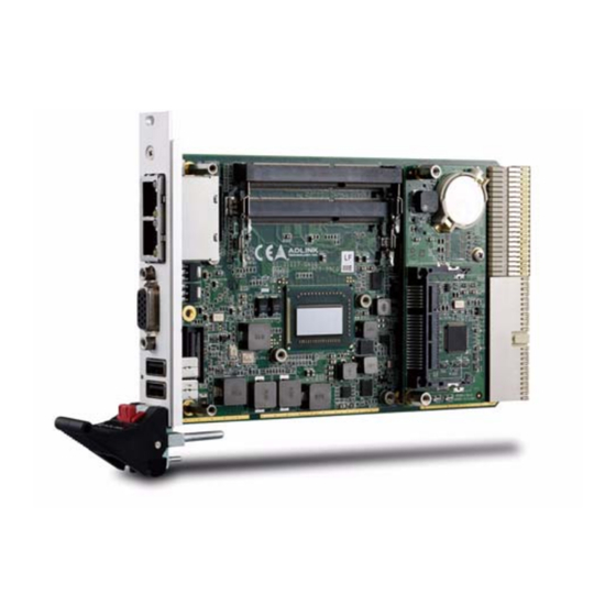
Intel® Core Processor CompactPCI Connector J1 Intel® QM67 PCH cPCI J2 (UHM/HM) CN4/5 Stacked SO-CDIMM socket LAN Dual Ethernet connectors DB-3610L2/DB-3970L2 VGA1 DB-15 VGA connector connector DB-3CFAST connector USB3 USB ports DB-3970L2 connector Figure 4-1: cPCI-3970 Series Board Layout Board Interfaces... -
Page 44: Cpci-3970 Blade Assembly Layout
4.2 cPCI-3970 Blade Assembly Layout This section describes the final assembly layout of the single slot cPCI-3970 Blade. DB-3CFAST Heatsink Figure 4-2: cPCI-3970 Blade Assembly Layout Battery CF or CFast socket Clear CMOS Jumper cPCI J2 (UHM/HM) Board Interfaces... -
Page 45: Cpci-3970D Blade Assembly Layout
cPCI-3970 4.3 cPCI-3970D Blade Assembly Layout The dual-slot width cPCI-3970D Blade is comprised of the cPCI-3970 single-slot main board and the DB-3610L2 riser card to expand I/O connectivity with PS/2, COM, 2x USB ports, Line-in, and Line-out ports . COM1 USB2 SATA0 USB3... -
Page 46: Cpci-3970G Blade Assembly Layout
4.4 cPCI-3970G Blade Assembly Layout The dual-slot width cPCI-3970D Blade is comprised of the cPCI-3970 single-slot main board and the DB-3970L2 riser card to expand I/O connectivity with PS/2, COM, USB ports, and 2x Dis- playPorts. COM2 2.5” SATA HDD SATA0 COM1 USB9... -
Page 47: Cpci-3970, Cpci-3970D, Cpci-3970G Faceplate
cPCI-3970 4.5 cPCI-3970, cPCI-3970D, cPCI-3970G Faceplate cPCI-3970 GP LED Reset Button Overheat LED HDD LED Power LED WDT LED cPCI-3970D PS/2 Line-in COM1 USB 2.0 KB/MS Line-out Reset Button GP LED HDD LED Overheat LED Power LED WDT LED cPCI-3970G PS/2 DisplayPorts KB/MS... -
Page 48: Cpci-3970S, Cpci-3970P, Cpci-3970U Front Panel
4.6 cPCI-3970S, cPCI-3970P, cPCI-3970U Front Panel cPCI-3970S cPCI-3970P cPCI-3970U Figure 4-6: cPCI-3970S, cPCI-3970P, cPCI-3970U Front Panel Layout Board Interfaces... -
Page 49: Cpci-3970L, Cpci-3970M, Cpci-3970Q Front Panel
cPCI-3970 4.7 cPCI-3970L, cPCI-3970M, cPCI-3970Q Front Panel cPCI-3970L cPCI-3970M cPCI-3970Q Figure 4-7: cPCI-3970L, cPCI-3970M, cPCI-3970Q Front Panel Layout Board Interfaces... -
Page 50: Table 4-1: Cpci-3970 Front Panel System Led Descriptions
System LEDs Color Condition Indication System is off Power Green/ System Power ready (PWGD) Green Post OK No Watchdog event Orange Blinking Watchdog event alert No CF/CFast/SATA HDD activity Blue Data read/write in process for CF/CFast/ Blinking SATA HDD CPU T temperature is under 100ºC Overheat junction... -
Page 51: Cpci-R3P00(T) Rtm Board Layout
cPCI-3970 4.8 cPCI-R3P00(T) RTM Board Layout LAN1/2 USB1 SATA2 USB10 SATA3 SATA4 VGA1 COM4 COM5 COM5* RS-232/422/485 port LAN1/2 Dual Ethernet ports (converted from USB) COM4 RS-232 port (Tx, Rx only) VGA1 VGA port SATA2/3/4 SATA ports USB1/10 USB ports CompactPCI connector Figure 4-8: cPCI-R3P00 RTM Board Layout *COM5 is incorrectly labeled COM3 on the A1 vers. -
Page 52: Cpci-R3P00(T) Rtm Faceplate
4.9 cPCI-R3P00(T) RTM Faceplate COM4 COM5 USB x2 GbE x2 Figure 4-9: cPCI-R3P00(T) RTM Front Panel Board Interfaces... -
Page 53: Connector Pin Assignments
cPCI-3970 4.10 Connector Pin Assignments USB Connectors Pin # Signal Name UV0- UV0+ Table 4-2: USB Pin Definition DB-15 VGA Connector Signal Name Pin # Pin # Signal Name Green Blue N.C. +5V. N.C. CRTDATA HSYNC VSYNC CRTCLK Table 4-3: VGA Pin Definition Board Interfaces... -
Page 54: Table 4-4: Rj-45 Gbe Pin Definitions
RJ-45 Gigabit Ethernet Connectors 10BASE-T/ Pin # 1000BASE-T 100BASE-TX LAN_TX0+ LAN_TX0- LAN_TX1+ — LAN_TX2+ — LAN_TX2- LAN_TX1- — LAN_TX3+ — LAN_TX3- Table 4-4: RJ-45 GbE Pin Definitions Speed Activity Speed LED Activity LED Status (Green/Orange) (Yellow) Network link is not established or system powered off Link 10 Mbps... -
Page 55: Table 4-6: Ps/2 Keyboard/Mouse Pin Definition
cPCI-3970 PS/2 Keyboard/Mouse Connector Pin # Signal Function KBDATA Keyboard Data MSDATA Mouse Data Ground Power KBCLK Keyboard Clock MSCLK Mouse Clock Table 4-6: PS/2 Keyboard/Mouse Pin Definition cPCI-3970D/P Serial Ports COM1 Connector (DB-9) Pin # RS-232 RS-422 RS-485(+) DCD-L TXD- TXD- TXD+... -
Page 56: Table 4-8: Cpci-3970D/P Com1 Mode Selection Switch Settings
COM1 Mode Selection Switches (SW1~SW4) These switches set the cPCI-3970D/P COM1 to RS-232 full modem, RS-422, RS-485, or RS-485+ half-duplex mode. Switches SW1~SW4 are located on the top edge of the DB-3610L2 board. RS-232 full modem is set by default. Mode RS-232 RS-422... -
Page 57: Table 4-9: Cpci-3970G/U Com1 (Rj-45) Pin Definition
cPCI-3970 cPCI-3970G/U Serial Ports The COM mode setting for cPCI-3970G/U models are set in the BIOS: “cPCI-3970G COM1/ 2 Output” on page 122. NOTE: NOTE: COM1 Connector (RJ-45) Pin # RS-232 RS-422 RS-485 DCD-L — — RTS-L TXD+ TXD+ DSR-L —... -
Page 58: Table 4-11: Rs-422/485 Adapter Dongle Pin Definition
The cPCI-3970G/U COM1 RS-422/485 pin definitions are differ- ent from the common DB-9 pin definitions. An RS-422/485 DB-9 male-female adapter dongle is provided to allow compatibility NOTE: NOTE: with common RS-422/485 pin definitions. RS-422/485 Adapter Dongle A DB-9 male-female adapter dongle is provided to allow com- patibility with common RS-422/485 pin definitions DB-9 (Female) DB-9 (Male) -
Page 59: Table 4-13: Cpci-3970G/U Com2 Pin Header Definition
cPCI-3970 COM2 Pin Header Pin # RS-232 RS-422 RS-485 DCD-L — — DSR-L — — RXD- — RTS-L TXD+ TXD+ TXD- TXD- CTS-L RXD+ — DTR-L — — RI-L — — Ground — — — — Table 4-13: cPCI-3970G/U COM2 Pin Header Definition cPCI-R3P00(T) RTM Serial Ports COM4 Connector (DB-9)) Pin #... -
Page 60: Table 4-15: Cpci-R3P00(T) Rtm Com5 Pin Definition
COM5 Connector (DB-9) The cPCI-R3P00(T) RTM COM5 RS-422/485 pin definitions are different from the common DB-9 pin definitions. An RS-422/485 DB-9 male-female adapter dongle is provided to allow compati- NOTE: NOTE: bility with common RS-422/485 pin definitions. See Pin # RS-232 RS-422 RS-485... -
Page 61: Table 4-17: Displayport Pin Definition
cPCI-3970 DisplayPort Connectors Pin # Signal Pin # Signal CN_DP0_P Ground CN_DP0_N CN_DP1_P Ground CN_DP1_N CN_DP2_P Ground CN_DP2_N CN_DP3_P Ground CN_DP3_N CN_CAD-L CN_CEC CN_AUX_P Ground CN_AUX_N DDP_HPD Ground P3V3 Table 4-17: DisplayPort Pin Definition Board Interfaces... -
Page 62: Table 4-18: Cpci-3970M 100-Pin I/O Connector Pin Definition
cPCI-3970M 100-pin I/O Connector (CN4) Pin # Signal Pin # Signal USB9_CN-N USB9_CN-P USB1_CN-N USB1_CN-P TMDS_I2C_DATA TMDS_I2C_CLK TMDSB_DATA2B TMDSB_DATA2 TMDSB_DATA1B TMDSB_DATA1 TMDSB_DATA0B TMDSB_DATA0 TMDSB_CLKB TMDSB_CLK P5V_DVI1 TMDSB_HPD NC TMDS_I2C_DATA TMDS_I2C_CLK TMDSB_DATA2B TMDSB_DATA2 TMDSB_DATA1B TMDSB_DATA1 TMDSB_DATA0B TMDSB_DATA0 TMDSB_CLKB TMDSB_CLK P5V_DVI2 TMDSB_HPD Table 4-18: cPCI-3970M 100-pin I/O Connector Pin Definition Board Interfaces... - Page 63 cPCI-3970 Pin # Signal Pin # Signal P5V_USB_1_9 P5V_USB_1_9 P5V_USB_1_9 P5V_USB_1_9 P5V_KBMS MSCLK_CN MSDATA_CN KBCLK_CN KBDATA_CN COM1_CTS-L_C COM1_RXD_CN COM1_TXD_CN COM1_RTS-L_CN COM1_DSR-L_C COM1_DTR-L_CN COM1_DCD-L_CN COM2_CTS-L_C COM2_RXD_CN COM2_TXD_CN COM2_RTS-L_CN COM2_DSR-L_C COM2_DTR-L_CN COM2_DCD-L_CN AGND_AU AGND_AU L_IN_R L_IN_L L_IN_JD AGND_AU HP_R HP_L HP_JD AGND_AU Table 4-18: cPCI-3970M 100-pin I/O Connector Pin Definition Board Interfaces...
-
Page 64: Table 4-19: Serial Ata Connector On Rtm Pin Definition
Serial ATA Connectors on RTM (CN4-R, CN5-R) Pin # Signal Table 4-19: Serial ATA Connector on RTM Pin Definition Board Interfaces... -
Page 65: Table 4-20: Serial Ata Connector On Db-3610/3970L2 Pin Def'n
cPCI-3970 Serial ATA Connector on DB-3610L2/3970L2 Pin # Signal Signal Power P13~P15 Table 4-20: Serial ATA Connector on DB-3610L2/3970L2 Pin Definition Board Interfaces... -
Page 66: Table 4-21: Compactflash Socket Pin Definition
CompactFlash Socket (on DB-3CF) Signal Name Pin# Pin# Signal Name DD11 DD12 DD13 DD14 DD15 CS1J CS3J SDIORJ SDIOWJ IRQ15 PCSEL BRSTDRVJ SDIORDY SDACKJ IDEACTJ DIAG IOIS16J DD10 Table 4-21: CompactFlash Socket Pin Definition Board Interfaces... -
Page 67: Table 4-22: Cfast Socket Pin Definition
cPCI-3970 CFast Socket (on DB-3CFAST) Pin # Signal Name Ground SATA_TX-P SATA_TX-N Ground SATA_RX-N SATA_RX-P Ground CFast_CDI Ground Ground CFast_LED1 CFast_LED2 P3V3 P3V3 Ground Ground CFast_CDO Table 4-22: CFast Socket Pin Definition Board Interfaces... -
Page 68: Table 4-23: Db-3610L2 Connector Pin Definition
DB-3610L2 Connector (CN1) Signal Name Pin # Pin # Signal Name USB2-N -12V USB2-P USB3-N HDA_SDIN0 USB3-P HDA_R_SDOUT SATA_ICH_RX-N0 HDA_R_SYNC SATA_ICH_RX-P0 HDA_R_BIT_CLK SATA_TX-P0 CK_L2_PCIE1-P SATA_TX-N0 CK_L2_PCIE1-N PCIE_TXN5 CK_L2_PCIE2-P PCIE_TXP5 CK_L2_PCIE2-N PCIE_RXN5 HDA_R_RST-L PCIE_RXP5 SPKR L2_PCIE_RST-L PCIE_RXN4 PCIE_RXP4 USB_2_3_OC-L COM1_DCD-L PCIE_TXN4 COM1_RI-L PCIE_TXP4 COM1_CTS-L... -
Page 69: Table 4-24: Db-3Cfast Connector Pin Definition
cPCI-3970 DB-3CFAST Connector (CN2) Signal Name Pin # Pin # Signal Name PCH_SPKR CLK33_TPM SIO_SPKR LPC_FRAME-L TPM_RST-L CN_VCC_RTC LPC_AD3 LPC_AD2 LPC_AD1 LPC_AD0 TPM_LPCPD PCH_SERIRQ TPM_CLKRUN TPM_GPIO SATA_PCH_RX-N0 SATA_PCH_RX-P0 SATA_PCH_TX-N0 SATA_PCH_TX-P0 CFast_CDI CFast_CDO P3V3 P3V3 Table 4-24: DB-3CFAST Connector Pin Definition Board Interfaces... -
Page 70: Table 4-25: Db-3970L2 Connector Pin Definition
DB-3970L2 Connector (CN3) Signal Name Pin # Pin # Signal Name RS232_COM2_SEL-L COM2_DCD-L COM2_RI-L COM2_CTS-L COM2_DTR-L COM2_RTS-L COM2_DSR-L COM2_SOUT COM2_SIN PCH_DDPD_AUXN PCH_DDPC_AUXN PCH_DDPD_AUXP PCH_DDPC_AUXP PCH_DDPD_0N PCH_DDPC_0N PCH_DDPD_0P PCH_DDPC_0P PCH_DDPD_1N PCH_DDPC_1N PCH_DDPD_1P PCH_DDPC_1P PCH_DDPD_2N PCH_DDPC_2N PCH_DDPD_2P PCH_DDPC_2P PCH_DDPD_3N PCH_DDPC_3N PCH_DDPD_3P PCH_DDPC_3P DDPD_CTRLCLK DDPC_CTRLCLK DDPD_CTRLDATA... -
Page 71: Table 4-26: Db-3Umc Connector Pin Definition
cPCI-3970 DB-3UMC Connector on DB-3610L2/3970L2 Signal Name Pin # Pin # Signal Name -12V +12V CK_PCIE1_P CK_PCIE1_N PCIE_TXN2 CK_PCIE2_P PCIE_TXP2 CK_PCIE2_N PCIE_R_RXN2 PCIE_R_RXP2 PCIE_RST# PCIE_R_RXN1 PCIE_R_RXP1 PCIE_TXN4 PCIE_TXP4 +3.3V +3.3V Table 4-26: DB-3UMC Connector Pin Definition Board Interfaces... -
Page 72: Table 4-27: Pmc Connector Pin Definitions
PMC Connector on DB-3UMC (JN1/2) Pin# JN1 Signal JN2 Signal PMC_TCK P12V N12V PMC_TRST-L PMC_TMS PCIX_INTA-L NC (PMC_TDO) PCIX_INTB-L PMC_TDI PCIX_INTC-L PMC_MOD-L1 PCIX_INTD-L PMC_MOD-L2 P3V3_PMCAUX P3V3 CLK66_PCIX_PMC PMC_RST-L PMC_MOD-L3 P3V3 PCIX_GNT-L0 PMC_MOD-L4 PCIX_REQ-L0 PMC_PME-L PMC_VIO PCIX_AD30 PCIX_AD31 PCIX_AD29 PCIX_AD28 PCIX_AD27 PCIX_AD26 PCIX_AD25 PCIX_AD24... - Page 73 cPCI-3970 Pin# JN1 Signal JN2 Signal PCIX_FRAME-L PCIX_TRDY-L PCIX_IRDY-L P3V3 PCIX_DEVSEL-L PCIX_STOP-L PCIX_PCIXCAP PCIX_PERR-L PCIX_LOCK-L P3V3 PCIX_SERR-L PCIX_PAR PCIX_CBE-L1 PMC_VIO PCIX_AD14 PCIX_AD15 PCIX_AD13 PCIX_AD12 PCIX_M66EN PCIX_AD11 PCIX_AD10 PCIX_AD9 PCIX_AD8 P3V3 PCIX_AD7 PCIX_CBE-L0 PCIX_AD6 P3V3 PCIX_AD5 PCIX_AD4 PMC_VIO PCIX_AD3 PCIX_AD2 PCIX_AD1 PCIX_AD0 PCIX_ACK64-L P3V3...
-
Page 74: Table 4-28: Xmc Connector Pin Definition
XMC Connector on DB-3UMC (JN3) Pin# 3.3V VPWR Not used PCIE_RST-L 3.3V VPWR Not used Not used 3.3V VPWR Not used +12V 3.3V VPWR Not used -12V Not used VPWR Not used Not used VPWR Not used 3.3V VPWR Not used Not used VPWR Not used... -
Page 75: Table 4-29: Compactpci J1 Connector Pin Definition
cPCI-3970 CompactPCI J1 Connector REQ64# ENUM# +3.3V CPCI_AD1 CPCI_VIO CPCI_AD0 ACK64# P3V3 CPCI_AD4 CPCI_AD3 CPCI_AD2 CPCI_AD7 P3V3 CPCI_AD6 CPCI_AD5 P3V3 CPCI_AD9 CPCI_AD8 CPCI_M66EN CPCI_CBE-L0 GND CPCI_AD12 CPCI_AD11 CPCI_AD10 P3V3 CPCI_AD15 CPCI_AD14 CPCI_AD13 GND CPCI_SERR-L P3V3 CPCI_PAR CPCI_CBE-L1 GND P3V3 CPCI_PERR-L GND GND CPCI_DEVSEL-L CPCI_PCIXCAP CPCI_STOP-L CPCI_LOCK-L GND P3V3... -
Page 76: Table 4-30: Compactpci J2 Connector Pin Definition
CompactPCI J2 Connector CLK6 2_ETH_B+ 1_ETH_D+ 1_ETH_B+ CLK5 2_ETH_B- 1_ETH_D- 1_ETH_B- 2_ETH_A+ 1_ETH_C+ 1_ETH_A+ 2_ETH_D+ 2_ETH_C+ 2_ETH_A- 1_ETH_C- 1_ETH_A- 2_ETH_D- 2_ETH_C- PRST# REQ6# GNT6# 4PE_CLK- 2_PE_CLK+ DEG# 4PE_CLK+ 2_PE_CLK- FAL# REQ5# GNT5# 3PE_CLK+ 1_PE_CLK+ 4_PE_CLKE# DDC_DAT 3PE_CLK- 1_PE_CLK- 3_PE_CLKE# DDC_CLK 4PE_RX00+ 1_PE_CLKE# 2_PE_CLKE#... -
Page 77: Table 4-31: Cpci-R3P00 Rj2 Connector Pin Definition
cPCI-3970 cPCI-R3P00 rJ2 Connector Pin Z 22 GND 21 GND 2_ETH_B+ 1_ETH_D+ 1_ETH_B+ 20 GND 2_ETH_B- 1_ETH_D- 1_ETH_B- 19 GND 2_ETH_A+ 1_ETH_C+ 1_ETH_A+ 18 GND 2_ETH_D+ 2_ETH_C+ 2_ETH_A- 1_ETH_C- 1_ETH_A- 17 GND 2_ETH_D- 2_ETH_C- 16 GND 15 GND 14 GND DDC_DAT 13 GND DDC_CLK... -
Page 78: Table 4-32: Cpci-R3P00T Rj2 Connector Pin Definition
cPCI-R3P00T rJ2 Connector Pin Z 22 GND 21 GND 20 GND 19 GND 18 GND 17 GND 16 GND 4PE_CLK- 2_PE_CLK+ 15 GND 4PE_CLK+ 2_PE_CLK- 14 GND 3PE_CLK+ 1_PE_CLK+ 4_PE_CLKE# DDC_DAT 13 GND 3PE_CLK- 1_PE_CLK- 3_PE_CLKE# DDC_CLK 12 GND 4PE_RX00+ 1_PE_CLKE# 2_PE_CLKE# RGB_BLUE... -
Page 79: Jumper Settings
cPCI-3970 4.11 Jumper Settings Load BIOS Default Jumper (JP1) The cPCI-3970 Load BIOS Default Jumper is located on the DB-3CF/CFast daughter board. To load the default BIOS settings, short pins 2-3 on JP1, then reinstall the jumper cap to pins 1-2. BIOS Setting Connection Normal... - Page 80 This page intentionally left blank. Board Interfaces...
-
Page 81: Getting Started
Processor blade installation to chassis RTM installation to chassis 5.1 CPU and Heatsink The cPCI-3970 Series come with CPU and heatsink pre-installed. Removal of heatsink/CPU by users is not recommended. Please contact your ADLINK service representative for assistance. Getting Started... -
Page 82: Memory Module Installation
5.2 Memory Module Installation The cPCI-3970 Series supports DDR3-1066/1333 ECC memory modules stacked-type SO-CDIMM sockets. SO-CDIMM modules have a 204-pin footprint and are notched to facilitate correct installation in the SO-DIMM sockets. At least one memory module will be pre-installed in the lower socket as shown below. - Page 83 cPCI-3970 Installing the Memory Modules Align the notch in the memory module with the key on the SO-CDIMM slot. Press down on the module until is it is prop- erly seated in the socket. Getting Started...
-
Page 84: Sata Drive Installation
5.3 SATA Drive Installation The cPCI-3970D/G 2-slot version and cPCI-3970P/U 3-slot version provide space to install a slim type 2.5" Serial-ATA storage drive. SATA Drive Installing a - cPCI-3970D/G(P/U) 1. Drive mounting brackets and screws are provided in the accessory kit. Secure the brackets to the SATA drive with the four M3 screws provided. -
Page 85: Compactflash Installation
cPCI-3970 5.4 CompactFlash Installation The CompactFlash socket is located on the DB-3CF daughter board mounted on layer-1. To install a CF card, orient the card so that the bottom side is facing up and align with the CF socket as shown. -
Page 86: Converting From Cf To Cfast Slot
5.5 Converting from CF to CFast Slot DB-3CFAST is an optional accessory for the cPCI-3970 series. To change the CF1 slot from CompactFlash to CFast, follow the instructions below. For cPCI-3970 models with 2 or 3 slots, the layer-2 and layer-3 daughter boards and front panel must first be removed. - Page 87 cPCI-3970 Removing the Layer-2 Daughter Board 1. Remove the screws on the front panel as shown below (6 screws on "D/P" model, 5 screws on the "G/U" model). cPCI-3970D cPCI-3970G 2. Remove the screw next to the handle on the solder side of the cPCI-3970.
- Page 88 3. Remove the 5 screws securing the DB-3970L2 or DB-3610L2 layer-2 daughter board to the blade assembly. 4. Remove the front panel from the blade assembly. 5. Lift the DB-3970L2 or DB-3610L2 daughter board to remove it from the blade assembly. Getting Started...
- Page 89 cPCI-3970 Installing the DB-3CFAST Daughter Board 1. Remove the three screws securing the DB-3CF daugh- ter board as shown and lift it from the blade assembly. 2. Install the DB-3CFAST daughter board by aligning it with the board-to-board connector (CN2) on the cPCI-3970 main board and pressing down firmly.
- Page 90 3. Secure the DB-3CFAST by tightening the three screws shown below. 4. Reinstall the layer-2 daughter board, front panel and layer-3 daughter board as required by reversing the steps described above. Getting Started...
-
Page 91: Pmc/Xmc Card Installation
cPCI-3970 5.6 PMC/XMC Card Installation The cPCI-3970P/U provides one PMC/XMC slot designed to sup- port 3.3V or 5V V(I/O) (default 3.3V) and 5V or 12V VPWR (default 5V). Before you install the PMC/XMC card on the cPCI-3970P/U, please make sure that the PMC V(I/O) jumper JPX2 and XMC VPWR jumper JPX1 have been correctly set (see page 65). - Page 92 2. Remove the DB-3UMC daughter board from the blade assembly by unscrewing the four screws securing it to the layer-2 daughter board as shown below. 3.3V Key 3. There is a 3.3V key on board by default, if the PMC/XMC card you wish to install is 5V signaling, please remove the key and set the PMC V(I/O) jumper JPX2 to the 5V setting (see “PMC V(I/O) Select Jumper on DB-3UMC...
- Page 93 cPCI-3970 4. Align the male connectors of the PMC/XMC card (com- ponent-side down) to the female connectors of the DB-3UMC and press down. 5. Secure the PMC/XMC card to the DB-3UMC by attach- ing four screws (provided with the card) from the under- side of the daughter board.
- Page 94 6. Align the male board-to-board connector (CN1) of the PMC/XMC assembly to the female board-to-board connec- tor (CN7) of the layer-2 daughter board and press down. 7. Secure the PMC/XMC assembly to the layer-2 daughter board using the four screws removed in Step 2 above. 8.
-
Page 95: Installing The Cpci-3970 To The Chassis
cPCI-3970 5.7 Installing the cPCI-3970 to the Chassis The cPCI-3970 may be installed in a system or peripheral slot of a 3U CompactPCI chassis. These instructions are for reference only. Refer to the user guide that comes with the chassis for more information. -
Page 96: Rtm Installation - Cpci-R3P00(T)
RTMs. Refer to previous sections for peripheral connectivity of all I/O ports on the RTM. When installing the cPCI-3970 Series and related RTMs, make sure the RTM is the correct matching model. You must install the correct RTM to enable functions (I/O inter- faces) on the rear panel. -
Page 97: Driver Installation
cPCI-3970 Driver Installation The cPCI-3970 drivers are available from the ADLINK All-In-One DVD at X:\cPCI\cPCI-3970\, or from the ADLINK website (http://www.adlinktech.com). ADLINK provides validated driv- ers for Windows XP Professional and Windows 7. We recommend using these drivers to ensure compatibility. The VxWorks BSP can be downloaded from the cPCI-3970 product page on the ADLINK website 6.1 cPCI-3970 Drivers... - Page 98 8. Install the audio driver and utilities by extracting and running the program in …\Audio\RealTek_High_Definition_Audio _WINXP_5.10.0.6029.zip. 9. Install the Intel® Management Engine Interface driver to remove the "question mark" from Other Devices in Windows Device Manager. The cPCI-3970 does not support Intel® Active Management Technology.
- Page 99 cPCI-3970 Select "Install from a list or specific location (Advanced)" and click Next. Extract the contents of …\cPCI-3970\Chipset\Intel _Management_Engine_Interface_AllOS_7.0.0.1144.zip. Select "Search for the best driver in these locations" and "Include this location in the search". Click Browse and navi- gate to the folder "MEI" where you extracted the contents of the zip file, and then click OK.
-
Page 100: Usb-To-Serial Converter Driver (Rtm)
6.2 USB-to-Serial Converter Driver (RTM) The COM5 serial port on the cPCI-R3P00(T) is converted from the USB3 port by a USB-to-serial converter (see “cPCI-R3P00 RTM” on page 17). To install the driver for the converter, follow the pro- cedure below. The installation consists of two parts: USB Serial Converter and USB Serial Port. - Page 101 cPCI-3970 4. Select "Install from a list or specific location (Advanced)" and click Next. 5. Extract the contents of …\cPCI-3970\COM\USB_Serial _Port_WINXP_32_WIN7_64_FTDI 2.8.8.0. Select "Search for the best driver in these locations" and "Include this location in the search". Click Browse and navigate to the folder where you extracted the contents of the zip file, and then click OK.
- Page 102 6. When notified that the software has not passed Windows Logo testing, click Continue Anyway. 7. When the USB Serial Converter driver installation has com- pleted, click Finish to close the wizard. Driver Installation...
- Page 103 cPCI-3970 8. The Found New Hardware Wizard will automatically open and ask you to install the software for USB Serial Port. Select Install from a list or specific location (Advanced) and click Next. 9. When notified that the software has not passed Windows Logo testing, click Continue Anyway.
-
Page 104: Lan Driver For Cpci-R3P00T
10.When the USB Serial Converter driver installation has com- pleted, click Finish to close the wizard. 6.3 LAN Driver for cPCI-R3P00T The GbE ports on the cPCI-R3P00T are supported by an Intel® 82580DB Gigabit Ethernet Controller (see “cPCI-R3P00T RTM” on page 18). Install the LAN drivers by extracting and running the program PROWin32.exe in …\cPCI\cPCI-R3P00(T)\INTEL 82580 Network driver\. -
Page 105: Utilities
cPCI-3970 Utilities 7.1 Watchdog Timer This section describes the operation of the cPCI-3970’s watchdog timer (WDT). The primary function of the WDT is to monitor the cPCI-3970's operation and to reset the system if a software appli- cation fails to function as programmed. The following WDT func- tions may be controlled using a software application: enabling and disabling set and get current configuration... - Page 106 Reset Watchdog Timer This command is used to reload the WDT. Action Byte Value Description NetFn/LUN Request Defined command Response Complete Code 00h means OK Set Watchdog Timer This command is used to start and restart the Watchdog Timer using the specified countdown value. Action Byte Value...
- Page 107 cPCI-3970 Action Byte Value Description Pre-timeout interval in Request 1h~ffh ( ‘1h’ based.) seconds. [7] - reserved [6] - reserved [5] - OEM [4] - SMS/OS [3] - OS Load Timer Use Expiration flags [2] - BIOS/POST clear [1] - BIOS FRB2 [0] - reserved 0b = leave alone 1b = clear timer use...
- Page 108 Action Byte Value Description [7] - reserved [6:4] - pre-timeout interrupt 000b = none 001b = SMI (optional) 010b = NMI / Diagnostic Interrupt (optional) 011b = Messaging Interrupt 100b,111b = reserved Timer Actions [3] - reserved [2:0] - timeout action 000b = no action 001b = Hard Reset 010b = Power Down...
-
Page 109: Figure 7-1: Example Procedure For Configuring The Wdt
cPCI-3970 Example WDT Programming Procedure Configuration of the watchdog timer is via serial interface. Detailed description of the WDT IPMI commands can be found above. The following example shows the procedure for configuring the WDT works over a serial console. See “Communications with IPMC” on page 137. - Page 110 2. Reload the WDT counter by using the raw IPMI command "Reset Watchdog Timer". "Reset Watchdog Timer" Command: [18 00 22] Successful response to Command: [1C 00 22 00] 3. Get the WDT configuration by using the "Get Watchdog Timer" command. "Get Watchdog Timer"...
-
Page 111: Using The Trusted Platform Module
cPCI-3970 7.2 Using the Trusted Platform Module This section describes the operation of the cPCI-3970’s Trusted Platform Module (TPM). Enabling TPM in BIOS The TPM is set to "Disabled" by default. Users wishing to use the TPM should enable it in BIOS as follows: 1. - Page 112 3. Set "TPM State" Enabled. Save settings and exit BIOS. Using the TPM Utility A utility for managing the TPM settings, the Infineon Security Plat- form Settings Tool, is provided with the TPM driver located on the All-In-One DVD in the following directory: X:\cPCI\cPCI- 3970\TPM.
- Page 113 cPCI-3970 2. The Infineon Security Platform Settings Tool is shown in the screen capture below. 3. Click on the "User Settings" tab, then follow the on screen instructions to build a security platform. Utilities...
- Page 114 4. Prepare a removable media to store important pass- words and data and follow the on screen instructions. Utilities...
-
Page 115: Bios Recovery
7.3 BIOS Recovery The cPCI-3970 Series features AMI® EFI BIOS with BIOS recov- ery. If the BIOS becomes corrupted and you are unable to boot your system, the system will sound 4 beeps. Follow the instruc- tions below to re-flash the BIOS and recover the system. - Page 116 6. During the BIOS recovery process, you will see the following: 7. After the flash update is completed, power down the system and restart. The system should now boot up normally. After BIOS recovery, follow the instructions in Section 7.4 BIOS Update to restore your original BIOS version.
-
Page 117: Bios Update
cPCI-3970 7.4 BIOS Update Follow the instructions below to update the BIOS or restore a pre- vious BIOS version. 1. Download the required BIOS file from the product website: www.adlinktech.com/PD/web/PD_detail.php?cKind=&pid=1013. 2. Prepare a DOS bootable floppy disk or USB flash drive and unzip the contents of the BIOS file to the disk 3. - Page 118 This page intentionally left blank. Utilities...
-
Page 119: Bios Setup Utility
cPCI-3970 BIOS Setup Utility The following chapter describes basic navigation for the AMI EFI BIOS setup utility. 8.1 Starting the BIOS To enter the setup screen, follow these steps: 1. Power on the motherboard 2. Press the < Delete > key on your keyboard when you see the following text prompt: <... - Page 120 Setup Menu The main BIOS setup menu is the first screen that you can navi- gate. Each main BIOS setup menu option is described in this user’s guide. The Main BIOS setup menu screen has two main frames. The left frame displays all the options that can be configured.
- Page 121 cPCI-3970 Navigation Note: There is a hot key legend located in the right frame on most setup screens. Keyboard Commands Enter Selects the highlighted option or submenu. < > The Left and Right "Arrow" keys allow you to select a setup screen.
-
Page 122: Main Setup
8.2 Main Setup When you first enter the Setup Utility, you will enter the Main setup screen. You can always return to the Main setup screen by select- ing the Main tab. There are two Main Setup options. They are described in this section. - Page 123 cPCI-3970 System Time/System Date Use this option to change the system time and date. Highlight Sys- tem Time or System Date using the < Arrow > keys. Enter new val- ues using the keyboard. Press the < Tab > key or the < Arrow > keys to move between fields.
-
Page 124: Advanced Bios Setup
8.3 Advanced BIOS Setup Select the Advanced tab from the setup screen to enter the Advanced BIOS Setup screen. You can select any of the items in the left frame of the screen, such as SuperIO Configuration, to go to the sub menu for that item. You can display an Advanced BIOS Setup option by highlighting it using the <... - Page 125 cPCI-3970 PCI Subsystem Settings PCI Latency Timer Value to be programmed into PCI Latency Timer Register. Options: 32 PCI Bus Clocks, 64 PCI Bus Clocks, 96 PCI Bus Clocks, 128 PCI Bus Clocks, 160 PCI Bus Clocks, 192 PCI Bus Clocks, 224 PCI Bus Clocks, 248 PCI Bus Clocks.
- Page 126 Trusted Computing Trusted computing is an industry standard to make personal com- puters more secure through a dedicated hardware chip, called a Trusted Platform Module (TPM). This option allows you to enable or disable the TPM support. BIOS Setup Utility...
- Page 127 cPCI-3970 CPU Configuration Hyper-Threading Enables/disables Hyper-Threading Technology. Active Processor Cores Number of cores to enable in each processor package. Options: All, 1, 2. Intel Virtualization Enables/disables Intel Virtualization Technology. BIOS Setup Utility...
- Page 128 SATA Configuration SATA Controllers This item specifies enables/disables the SATA Controllers. SATA Mode The SATA interface can be configured as a legacy IDE, RAID and AHCI mode. BIOS Setup Utility...
- Page 129 cPCI-3970 USB Configuration Legacy USB Support Legacy USB Support refers to USB mouse and keyboard sup- port. Normally if this option is not enabled, any attached USB mouse or keyboard will not become available until a USB com- patible operating system is fully booted with all USB drivers loaded.
- Page 130 Device Power-up Delay Maximum time the device will take before it properly reports itself to the Host Controller. "Auto" uses these default values: for a Root port it is 100ms, for a Hub port the delay is taken from the Hub descriptor. Super IO Configuration Serial Port 1/2/3/4 Configuration Each sub-menu allows you to Enable/Disable and set the...
- Page 131 cPCI-3970 PC Health Configuration BIOS Setup Utility...
- Page 132 Console Redirection The settings specify how the host computer and the remote computer will exchange data. Both computers should have the same or compatible settings. Terminal Type VT-UTF8 is the preferred terminal type for out-of-band man- agement. The next best choice is VT100+ and then VT100. Options: VT100, VT100+, VT-UTF8, ASNI.
- Page 133 cPCI-3970 Communication with slow devices may require more than 1 stop bit. Set this value to 1 or 2. Flow Control Set this option to select Flow Control for console redirection. The settings for this value are None, Hardware, Software. Terminal Resolution Remote Terminal Resolution.
-
Page 134: Chipset Configuration
8.4 Chipset Configuration Select the Chipset tab from the setup screen to enter the Chipset BIOS Setup screen. You can select any of Chipset BIOS Setup options by highlighting it using the < Arrow > keys. The Chipset BIOS Setup screen is shown below. System Agent (SA) Configuratio Enables/disables Intel®... - Page 135 cPCI-3970 Graphics Configuration Primary Display Allows you to select which graphics controller to use as the pri- mary boot device. Configuration options: IGD, PCI/IGD, PCI/PEG, PEG/IGD, PEG/PCI. Internal Graphics Allows you to select enable/disable.the internal graphics. DVMT Pre-Allocated Select DVMT 5.0 Pre-Allocated (fixed) Graphics Memory size used by the internal graphics device.
- Page 136 PCH-IO Configuration LAN1, LAN2, VGA Output Sets the LAN1/LAN2/VGA output to Front/Rear. cPCI-3970G COM1/ 2 Output Sets the cPCI-3970G COM1/2 mode. Options: RS232, RS422/RS485. The cPCI-3970G COM1/2 Output BIOS setting is only used for cPCI-3970G/U models. The COM mode setting for cPCI-3970D/P models must be set using the “COM1 Mode NOTE: NOTE:...
- Page 137 cPCI-3970 USB Configuration EHCI1/2 Controller 1 USB 2.0 (EHCI) support. Set this value to Enabled/Disabled. BIOS Setup Utility...
-
Page 138: Boot Configuration
8.5 Boot Configuration Select the Boot tab from the setup screen to enter the Boot Con- figuration screen. You can select any of the items in the left frame of the screen to go to the sub menu for that item. You can display a Boot Configuration option by highlighting it using the <... -
Page 139: Security Setup
cPCI-3970 8.6 Security Setup Administrator Password Use this option to set a password for administrators with full con- trol of the BIOS setup utility. User Password Use this option to set a password for users with limited access to the BIOS setup utility. BIOS Setup Utility... -
Page 140: Save & Exit
8.7 Save & Exit Select the Save & Exit tab from the setup screen to enter the Save & Exit setup screen. You can display a Save & Exit BIOS setup option by highlighting it using the < Arrow > keys. The Save & Exit BIOS setup screen is shown below. - Page 141 cPCI-3970 Save Changes Save changes made so far to any of the setup options. Discard Changes Discard changes made so far to any of the setup options. Restore Defaults Restore/Load Defaults values for all the setup options. Boot Override Use the up/down arrow keys to highlight a boot device to immedi- ately exit the BIOS Setup and boot from the selected device.
- Page 142 This page intentionally left blank. BIOS Setup Utility...
-
Page 143: Ipmi User Guide
cPCI-3970 IPMI User Guide 9.1 Introduction This chapter is written for those who already have a basic under- standing of the newest implementation of the baseboard manage- ment controller (BMC) of the Intelligent Platform Management Interface (IPMI) specification rev. 2.0. It also describes the OEM extension IPMI command usages which are not listed in the IPMI specification. - Page 144 IPMI Command NetFn CMD Description Spec This is a broadcast version of the ‘Get Broadcast "Get Device ID’ command that is provided for 17.9 Device ID" the ‘discovery’ of Intelligent Devices on the IPMB IPMI Messaging Support Commands The Send Message command is used for bridging IPMI messages between Send Message 18.7...
- Page 145 cPCI-3970 IPMI Command NetFn CMD Description Spec Sensor Device Commands This command returns general Get Device SDR 29.2 information about the collection of Info sensors in a Dynamic Sensor Device. The ‘Get Device SDR’ command allows SDR information for sensors for a Sensor Get Device SDR 29.3 Device (typically implemented...
- Page 146 IPMI Command NetFn CMD Description Spec This command returns the present reading for sensor. The sensor device Get Sensor may return a stored version of a 29.14 Reading periodically updated reading, or the sensor device may scan to obtain the reading after receiving the request.
-
Page 147: Oem Commands Summary Table
cPCI-3970 9.3 OEM Commands Summary Table Command NetFn Code Cmd Code System Life Time App (18h) Statistics of Power Cycle App (18h) Voltage Detection from Internal Sensor App (18h) Thermal Detection App (18h) Voltage Detection from External App (18h) Sensor System Power Status App (18h) BIOS Operation Status... - Page 148 Action Byte Value Description Complete Code 00h means OK The counter is added byt Reset Times pushing reset button. LS on Power Button byte last. The counter is added by Reset Times system reset request on on Payload payload. LS byte last. Response The counter is added by Reset Times...
- Page 149 cPCI-3970 Thermal Detection This command is used to get temperatures from external sensor components. Action Byte Value Description NetFn/LUN Defined command Request 01h : CPU Temperature 01h~02h 02h : System Temperature Complete Code 00h means OK Assigned It gets digital raw data. The Response Temperature value practical value can be...
- Page 150 System Power Status This command is used to detect system power status via GPIO pin signal on IPMC chip. Action Byte Value Description NetFn/LUN Request Defined command Complete Code 00h means OK Response 00: Power Fail 00h~01h 01 : Power OK BIOS Operation Status This command is used to get BIOS operation status.
-
Page 151: Compactpci Address Map
cPCI-3970 9.4 CompactPCI Address Map Since more than one system may be installed in a single chassis, we allocate each IPMB address based on GA input as peripheral cards. The CompactPCI Peripheral Address Mapping Table is given below. CompactPCI Peripheral Address Mapping Geo. -
Page 152: Ipmi Sensors List
9.6 IPMI Sensors List Sensor Reading Value of Sensor Normal Sensor name IPMI Get Sensor Reading Number Reading Command Timeout action: 000b = no action 001b = Hard Reset BMC Watchdog 000b = Power Down 011b = Power Cycle 100b - 111b = reserved 3.3V 3.3 V Raw data of 3.3V sensor... -
Page 153: Relevant Documents
cPCI-3970 Sensor Reading Value of Sensor Normal Sensor name IPMI Get Sensor Reading Number Reading Command BIOS status: 00b : Not Ready. 01b : BIOS Reset. 02b : ROM Check. 03b : Initiate Hardware. BIOS POST OK 04b : Enter BIOS Menu. 05b : Start BIOS firmware burning process. - Page 154 This page intentionally left blank. IPMI User Guide...
-
Page 155: Important Safety Instructions
cPCI-3970 Important Safety Instructions For user safety, please read and follow all instructions, WARNINGS, CAUTIONS, and NOTES marked in this manual and on the associated equipment before handling/operating the equipment. Read these safety instructions carefully. Keep this user’s manual for future reference. Read the specifications section of this manual for detailed information on the operating environment of this equipment. - Page 156 Never attempt to fix the equipment. Equipment should only be serviced by qualified personnel. A Lithium-type battery may be provided for uninterrupted, backup or emergency power. Risk of explosion if battery is replaced with one of an incorrect type. Dispose of used batteries appropriately. WARNING: Equipment must be serviced by authorized technicians when:...
-
Page 157: Getting Service
5215 Hellyer Avenue, #110, San Jose, CA 95138, USA Tel: +1-408-360-0200 Toll Free: +1-800-966-5200 (USA only) Fax: +1-408-360-0222 Email: info@adlinktech.com ADLINK Technology (China) Co., Ltd. Address: (201203) 300 Fang Chun Rd., Zhangjiang Hi-Tech Park, Pudong New Area, Shanghai, 201203 China Tel: +86-21-5132-8988 Fax:... - Page 158 84 Genting Lane #07-02A, Cityneon Design Centre, Singapore 349584 Tel: +65-6844-2261 Fax: +65-6844-2263 Email: singapore@adlinktech.com ADLINK Technology Singapore Pte. Ltd. (Indian Liaison Office) Address: 1st Floor, #50-56 (Between 16th/17th Cross) Margosa Plaza, Margosa Main Road, Malleswaram, Bangalore-560055, India Tel: +91-80-65605817, +91-80-42246107 Fax: +91-80-23464606 Email: india@adlinktech.com...
Need help?
Do you have a question about the cPCI-3970 series and is the answer not in the manual?
Questions and answers