
Related Manuals for Quectel EM06 Series


Summary of Contents for Quectel EM06 Series
- Page 1 EM06 Series Hardware Design LTE-A Module Series Version: 1.4 Date: 2020-12-21 Status: Released www.quectel.com...
- Page 2 To the maximum extent permitted by law, Quectel excludes all liability for any loss or damage suffered in connection with the use of the functions and features under development, regardless of whether such loss or damage may have been foreseeable.
- Page 3 EM06 Series Hardware Design Copyright The information contained here is proprietary technical information of Quectel. Transmitting, reproducing, disseminating and editing this document as well as using the content without permission are forbidden. Offenders will be held liable for payment of damages. All rights are reserved in the event of a patent grant or registration of a utility model or design.
-
Page 4: About The Document
LTE-A Module Series EM06 Series Hardware Design About the Document Revision History Version Date Author Description King MA/ 2018-07-17 Initial Wison HE Updated CA feature of EM06-A (Table 1). Updated Internet protocol features of EM06 (Table Deleted information about USB 3.0 and changed USB 3.0 pins into NC pins (Figure 2 and Table 4). - Page 5 LTE-A Module Series EM06 Series Hardware Design Deleted the information about EM06-LA. Added a reference design for power supply circuit with buck DC-DC converter (Figure 5). Updated the current consumption of EM06-E in Eysen Wang/ Chapter 31. 2020-12-21 Archibald JIANG Deleted M.2 Socket 2 USB 3.0-Based Pinout row in...
-
Page 6: Table Of Contents
LTE-A Module Series EM06 Series Hardware Design Contents About the Document ........................... 3 Contents ............................... 5 Table Index ..............................7 Figure Index ..............................8 Introduction ............................9 1.1. Safety Information ........................10 Product Concept ..........................11 2.1. General Description ........................11 2.2. - Page 7 LTE-A Module Series EM06 Series Hardware Design Antenna Connection .......................... 44 5.1. Main/Rx-diversity/GNSS Antenna Connectors ................. 44 5.1.1. Antenna Connectors ...................... 44 5.1.2. Operating Frequencies....................45 5.1.2.1. Cellular Operating Frequencies ................45 5.1.2.2. GNSS Operating Frequencies ................47 5.2. Antenna Installation ........................47 5.2.1.
- Page 8 EM06 Series Hardware Design Table Index Table 1: Frequency Bands, CA Combinations and GNSS Types Supported ..........11 Table 2: Key Features of EM06 Series ...................... 12 Table 3: Definition of I/O Parameters ......................18 Table 4: Pin Description ..........................18 Table 5: Overview of Operating Modes ......................
- Page 9 Figure 29: Connect Receptacle and Mating Plug Using Ø 1.13 mm Coaxial Cable ......... 50 Figure 30: Thermal Dissipation Area on Bottom Side of Module (Top View) ..........62 Figure 31: Mechanical Dimensions of EM06 Series (Unit: mm) ..............63 Figure 32: Standard Dimensions of M.2 Type 3042-S3 (Unit: mm) ............64 Figure 33: M.2 Nomenclature ........................
-
Page 10: Introduction
LTE-A Module Series EM06 Series Hardware Design Introduction This document defines the EM06 series module and describes its air and hardware interfaces which connect to your applications. It helps you quickly understand EM06 series’ interface specifications, electrical and mechanical details, as well as other related information. -
Page 11: Safety Information
The following safety precautions must be observed during all phases of operation, such as usage, service or repair of any cellular terminal or mobile incorporating EM06 series module. Manufacturers of the cellular terminal should notify users and operating personnel of the following safety information by incorporating these guidelines into all manuals of the product. -
Page 12: Product Concept
With standard PCI Express M.2 interfaces, the series supports data connection on LTE-FDD, LTE-TDD, DC-HSDPA, DC-HSPA+, HSDPA, HSUPA and WCDMA networks. EM06 series supports embedded operating systems such as Windows, Linux and Android, and also carries GNSS and voice functionality to meet specific application demands. -
Page 13: Key Features
QZSS NOTES The GNSS function is optional. EM06 series modules (EM06-E/EM06-J/EM06-A) come in two versions: Telematics and Data-only. The Telematics version supports voice and data functions, while the Data-only version only supports the data function. LTE-FDD B29 and B32 are supported only for Rx and secondary component carrier(s). - Page 14 LTE-A Module Series EM06 Series Hardware Design ⚫ Class 3 (23 dBm ± 2 dB) for LTE-FDD bands ⚫ Transmitting Power Class 3 (23 dBm ± 2 dB) for LTE-TDD bands ⚫ Class 3 (24 dBm +1/-3 dB) for WCDMA ⚫...
- Page 15 GNSS Features Protocol: NMEA 0183 ⚫ Data rate: 1 Hz ⚫ Compliant with 3GPP TS 27.007, 27.005 and Quectel enhanced AT AT Commands commands ⚫ Size: (42.0 ± 0.15) mm × (30.0 ± 0.15) mm × (2.3 ± 0.10) mm Physical Characteristics ⚫...
-
Page 16: Functional Diagram
Figure 1: Functional Diagram 2.4. Evaluation Board To help you develop applications conveniently with EM06 series modules, Quectel supplies the evaluation board (M.2 EVB), USB to RS-232 converter cable, USB type-C cable, earphone, antennas and other peripherals to control or test the module. For more details, please refer to document [1]. -
Page 17: Application Interfaces
LTE-A Module Series EM06 Series Hardware Design Application Interfaces The physical connections and signal levels of EM06 series comply with PCI Express M.2 specifications. This chapter mainly describes the definition and application of the following interfaces, signals and pins of the modules: ⚫... -
Page 18: Pin Assignment
LTE-A Module Series EM06 Series Hardware Design 3.1. Pin Assignment The following figure shows the pin assignment of EM06 series. The module and antenna connectors are on the top side. Pin Name Pin Name CONFIG_2 CONFIG_1 RESET# USIM1_DET ANTCTL3 RESERVED... -
Page 19: Pin Description
LTE-A Module Series EM06 Series Hardware Design 3.2. Pin Description The following tables define and describe the pins of EM06 series on a 75-pin application. Table 3: Definition of I/O Parameters Type Description Digital Input Digital Output Bidirectional Open Drain... - Page 20 LTE-A Module Series EM06 Series Hardware Design Airplane mode control W_DISABLE1# 1.8/3.3 V power domain Active low USB_DM USB 2.0 differential data bus (-) An open collector and active low signal WWAN_LED# Allows the module to provide RF 3.3 V power domain...
- Page 21 LTE-A Module Series EM06 Series Hardware Design Ground PCM data frame synchronization PCM_SYNC 1.8 V power domain signal USIM1_RST (U)SIM1 card reset 1.8/3.0 V power domain USIM1_CLK (U)SIM1 card clock 1.8/3.0 V power domain Ground Pulled up to USIM1_DATA (U)SIM1 card data...
- Page 22 LTE-A Module Series EM06 Series Hardware Design Ground I2C serial data I2C_SDA Used for external codec Ground I2C serial clock I2C_SCL Used for external codec ANTCTL0 Antenna tuner control 1.8 V power domain RESERVED Reserved ANTCTL1 Antenna tuner control 1.8 V power domain...
-
Page 23: Operating Modes
⚫ NOTE Please keep all NC, reserved and unused pins unconnected. 3.3. Operating Modes The table below summarizes different operating modes of EM06 series. Table 5: Overview of Operating Modes Mode Details The module has registered on network and is ready to send and Idle receive data, its software being active. -
Page 24: Power Supply
LTE-A Module Series EM06 Series Hardware Design 3.4. Power Supply The following table defines VCC and GND pins. Table 6: Definition of VCC and GND Pins Pin Name Pin No. Power Domain Description – 2, 4, 70, 72, 74 3.135 4.4 V... -
Page 25: Reference Design Of Power Supply
LTE-A Module Series EM06 Series Hardware Design Module 1 uF 220 uF 100 nF 33 pF 10 pF 5.1 V Figure 4: Reference Design of VCC 3.4.2. Reference Design of Power Supply Power design is critical as the module’s performance largely depends on its power source. The power supply should be capable of providing a sufficient current of 2 A at least. -
Page 26: Turn On/Off
LTE-A Module Series EM06 Series Hardware Design 3.5. Turn On/Off 3.5.1. Turn On the Module Driving the FULL_CARD_POWER_OFF# pin to high level will power on the module. The following table shows the definition of FULL_CARD_POWER_OFF#. Table 7: Pin Definition of FULL_CARD_POWER_OFF# Pin Name Pin No. - Page 27 LTE-A Module Series EM06 Series Hardware Design A reference circuit is shown in the following figure. Module 3.3 V FULL_CARD_POWER_ OFF# Figure 7: Turn on the Module Automatically The power-on scenario is illustrated in the following figure. NOTE RESET# 1.19 V FULL_CARD_POWE R_OFF# 1.8 V or 3.0 V...
-
Page 28: Turn Off The Module
LTE-A Module Series EM06 Series Hardware Design 3.5.2. Turn Off the Module 3.5.2.1. Turn Off through FULL_CARD_POWER_OFF# Driving the FULL_CARD_POWER_OFF# pin to low level will turn off the module. The power-off scenario is illustrated in the following figure. RESET# (H) - Page 29 LTE-A Module Series EM06 Series Hardware Design min = 1.3 V max = 0.5 V An open collector driver or button can be used to control the RESET# pin. RESET# 4.7K Reset pulse Figure 10: Reference Design of Resetting Using Driving Circuit...
-
Page 30: U)Sim Interfaces
When (U)SIM2 card is present, it USIM2_DET detection. is at high level. Active high. When (U)SIM2 card is absent, it is at low level. EM06 series modules support (U)SIM card hot-plug via the USIM_DET pin, a level trigger pin normally EM06_Series_Hardware_Design 29 / 69... - Page 31 LTE-A Module Series EM06 Series Hardware Design short-circuited to ground when no (U)SIM card inserted. When a (U)SIM card gets inserted, the pin will change from low to high level with a rising edge indicating the insertion of a (U)SIM card; when the card is removed, the pin will return to low level with a falling edge indicating the removal of card.
- Page 32 LTE-A Module Series EM06 Series Hardware Design Normally Open (U)SIM Card Connector: ⚫ When the (U)SIM card is absent, the switch is open and USIM_DET is at low level. ⚫ When the (U)SIM card is inserted, the switch is closed and USIM_DET is at high level.
- Page 33 LTE-A Module Series EM06 Series Hardware Design When AT+QSIMDET=1, 1 is set, the timing of hot plugging is illustrated by the following figure. USIM_ DET 450 ms 0.1 ms 10 ms USIM_ VDD ta + 5 2 u s USIM_ DATA 1.5 ms...
-
Page 34: Usb Interface
EM06 Series Hardware Design 3.8. USB Interface Each EM06 series module provides one integrated Universal Serial Bus (USB) interface which complies with USB 2.0 specifications and supports high speed (480 Mbps) and full speed (12 Mbps) modes on USB 2.0. The USB interface is used for AT command communication, data transmission, GNSS NMEA sentences output, software debugging, firmware upgrade and voice over USB*. -
Page 35: Pcm And I2C Interfaces
If possible, reserve a 0 ohm resistor on USB_DP and USB_DM lines respectively. NOTE “*” means under development. 3.9. PCM and I2C Interfaces EM06 series modules support audio communications via Pulse Code Modulation (PCM) digital interface and I2C interface. The PCM interface supports the following modes: ⚫... - Page 36 LTE-A Module Series EM06 Series Hardware Design The module supports 16-bit linear data format. The following two figures show respectively the timing relationship between 8 kHz PCM_SYNC and 2048 kHz PCM_CLK in the primary mode and that between 8 kHz PCM_SYNC and 256 kHz PCM_CLK in the auxiliary mode.
- Page 37 LTE-A Module Series EM06 Series Hardware Design The following table shows the pin definition of PCM and I2C interfaces which can be applied to audio codec design. Table 11: Pin Definition of PCM and I2C Interfaces Pin Name Pin No.
-
Page 38: Control And Indication Interface
It is recommended to add an RC (R = 22 Ω, C = 22 pF) circuit on the PCM lines, especially for PCM_CLK. EM06 series module works as a master device pertaining to I2C interface. 3.10. Control and Indication Interface The following table shows the pin definition of control and indication interfaces. -
Page 39: Wwan_Led
LTE-A Module Series EM06 Series Hardware Design Table 13: Airplane Mode Controlled by Hardware W_DISABLE1# RF Function Status Module Operating Mode High level RF enabled Normal mode Low level RF disabled Airplane mode The software approach is by executing the command AT+CFUN, which has the same function with the W_DISABLE1# signal. -
Page 40: Wake_On_Wan
LTE-A Module Series EM06 Series Hardware Design The following table shows the RF status indicated by WWAN_LED# signal. Table 15: Network Status Indication by WWAN_LED# Signal WWAN_LED# Level Description Low Level (LED ON) RF function is turned on. RF function is turned off if any of the following circumstances occurs: ⚫... -
Page 41: Dpr Signal
LTE-A Module Series EM06 Series Hardware Design VCC from the Host Host Module WAKE_ON_WAN# Figure 24: Reference Design of WAKE_ON_WAN# 3.10.4. DPR Signal The module provides a DPR (Dynamic Power Reduction) signal for body SAR (Specific Absorption Rate) detection. The signal is sent by a host system proximity sensor to the module to provide an input trigger which will reduce the output power in the radio transmission. -
Page 42: Configuration Pins
LTE-A Module Series EM06 Series Hardware Design Table 18: Pin Definition of Antenna Tuner Control Interface Pin Name Pin No. Description Comment ANTCTL0 Antenna tuner control 1.8 V power domain ANTCTL1 Antenna tuner control 1.8 V power domain ANTCTL2 Antenna tuner control 1.8 V power domain... -
Page 43: Gnss Receiver
GNSS Receiver 4.1. General Description The EM06 series module includes a fully integrated global navigation satellite system solution that supports Gen8C-Lite of Qualcomm (GPS, GLONASS, BeiDou/Compass, Galileo and QZSS). The module supports standard NMEA-0183 protocol, and outputs NMEA sentences at 1 Hz data update rate via USB interface by default. - Page 44 LTE-A Module Series EM06 Series Hardware Design Autonomous Hot start @open sky XTRA enabled Accuracy Autonomous CEP-50 (GNSS) @open sky NOTES Tracking sensitivity: the minimum GNSS signal power at which the module can maintain locked - keep positioning for at least 3 minutes continuously.
-
Page 45: Antenna Connection
EM06 Series Hardware Design Antenna Connection The EM06 series module is mounted with three 2 mm × 2 mm antenna connectors (receptacles) for external antenna connection: a Main antenna connector, a Rx-diversity antenna connector which is used to resist the fall of signals caused by high speed movement and multipath effect, and a GNSS antenna connector. -
Page 46: Operating Frequencies
LTE-A Module Series EM06 Series Hardware Design 5.1.2. Operating Frequencies 5.1.2.1. Cellular Operating Frequencies Table 22: EM06-E Operating Frequencies 3GPP Band Transmit Receive Unit WCDMA B1 1920–1980 2110–2170 WCDMA B3 1710–1785 1805–1880 WCDMA B5 824–849 869–894 WCDMA B8 880–915 925–960 LTE-FDD B1 1920–1980... - Page 47 LTE-A Module Series EM06 Series Hardware Design WCDMA B6 830–840 875–885 WCDMA B8 880–915 925–960 WCDMA B19 830–845 875–890 LTE-FDD B1 1920–1980 2110–2170 LTE-FDD B3 1710–1785 1805–1880 LTE-FDD B8 880–915 925–960 LTE-FDD B18 815–830 860–875 LTE-FDD B19 830–845 875–890 LTE-FDD B26 814–849...
-
Page 48: Gnss Operating Frequencies
LTE-A Module Series EM06 Series Hardware Design LTE-FDD B30 2305–2315 2350–2360 LTE-FDD B66 1710–1780 2110–2200 LTE-TDD B41 2496–2690 2496–2690 NOTES LTE-FDD B29 and B32 are supported only for Rx and secondary component carrier(s). 2. “*” means under development. 5.1.2.2. GNSS Operating Frequencies The following table shows frequency specifications of the GNSS antenna connector. -
Page 49: Antenna Connectors And Mating Plugs
LTE-A Module Series EM06 Series Hardware Design Passive antenna gain: > 0 dBi VSWR: ≤ 2 Efficiency: > 30 % Max Input Power: 50 W Input Impedance: 50 Ω Cable insertion loss: < 1 dB WCDMA/LTE (WCDMA B5/B6/B8/B19, LTE B5/B8/B12/B13/B18/B19/B20/B26/B28/B29) Cable insertion loss: <... - Page 50 LTE-A Module Series EM06 Series Hardware Design Table 27: Major Specifications of Antenna Connectors Item Specification Nominal Frequency Range DC to 6 GHz 50 Ω Nominal Impedance Temperature Rating -40 ° C to +85 ° C Meet the requirements of: –...
- Page 51 LTE-A Module Series EM06 Series Hardware Design The following figure illustrates the connection between the receptacle antenna connector on EM06 series and the mating plug using a Ø 0.81 mm coaxial cable. Figure 28: Connect Receptacle and Mating Plug Using Ø 0.81 mm Coaxial Cable The following figure illustrates the connection between the receptacle antenna connector on EM06 series and the mating plug using a Ø1.13 mm coaxial cable.
-
Page 52: Electrical, Reliability And Radio Characteristics
Voltage at Digital Pins -0.3 6.2. Power Supply Requirements The typical input voltage of EM06 series is 3.7 V, as specified by PCIe M.2 Electromechanical Spec Rev1.0. The following table shows the power supply requirements of the module. Table 29: Power Supply Requirements... -
Page 53: I/O Requirements
LTE-A Module Series EM06 Series Hardware Design 6.3. I/O Requirements Table 30: I/O Requirements Parameter Description Min. Max. Unit Input high voltage 0.7 × V + 0.3 DD18 DD18 Input low voltage -0.3 0.3 × V DD18 Output high voltage - 0.5... - Page 54 LTE-A Module Series EM06 Series Hardware Design LTE-TDD PF = 64 (USB disconnected) 4.54 LTE-TDD PF = 128 (USB disconnected) 3.91 LTE-TDD PF = 256 (USB disconnected) 3.59 WCDMA PF = 64 (USB disconnected, band 1) 22.1 WCDMA PF = 64 (USB connected, band 1) 26.27...
- Page 55 LTE-A Module Series EM06 Series Hardware Design LTE-TDD B40 CH39150 @ 23.6 dBm LTE-TDD B41 CH40740 @ 23.6 dBm LTE-FDD B1 + B1 @ 21.8 dBm LTE-FDD B1 + B5 @ 21.7 dBm LTE-FDD B1 + B8 @ 21.8 dBm LTE-FDD B1 + B20 @ 21.9 dBm...
- Page 56 LTE-A Module Series EM06 Series Hardware Design WCDMA B8 CH3012 @ 22.9 dBm Table 32: EM06-J Current Consumption Parameter Description Conditions Typ. Unit μA OFF state Power down AT+CFUN=0 (USB disconnected) 2.96 WCDMA PF = 64 (USB disconnected) 3.76 Sleep state WCDMA PF = 128 (USB disconnected) 3.29...
- Page 57 LTE-A Module Series EM06 Series Hardware Design WCDMA B19 HSUPA CH738 @ 22.4 dBm LTE-FDD B1 CH300 @ 23.3 dBm LTE-FDD B3 CH1575 @ 23.1 dBm LTE-FDD B8 CH3625 @ 24.1 dBm LTE data LTE-FDD B18 CH5925 @ 24.2 dBm transfer LTE-FDD B19 CH6075 @ 23.4 dBm...
- Page 58 LTE-A Module Series EM06 Series Hardware Design Table 33: EM06-A Current Consumption Parameter Description Conditions Typ. Unit μA OFF state Power down AT+CFUN=0 (USB disconnected) 2.96 WCDMA PF = 64 (USB disconnected) 3.76 Sleep state WCDMA PF = 128 (USB disconnected) 3.29...
-
Page 59: Rf Output Power
WCDMA voice WCDMA B4 CH1638 @ 23.2 dBm call WCDMA B5 CH4407 @ 22.9 dBm 6.5. RF Output Power The following table shows the RF output power of EM06 series modules. Table 34: RF Output Power Frequency Max. Min. WCDMA bands 24 dBm +1/-3 dB <... -
Page 60: Rf Receiving Sensitivity
LTE-A Module Series EM06 Series Hardware Design 6.6. RF Receiving Sensitivity The following tables show conducted RF receiving sensitivity of EM06 series modules. Table 35: EM06-E Conducted RF Receiving Sensitivity Primary Diversity SIMO SIMO Frequency (Typ.) (Typ.) (Typ.) (Worst Case) WCDMA B1 -109.5 dBm... - Page 61 LTE-A Module Series EM06 Series Hardware Design WCDMA B6 -108 dBm -109 dBm -111 dBm -106.7 dBm WCDMA B8 -109 dBm -109 dBm -111 dBm -103.7 dBm WCDMA B19 -109 dBm -109 dBm -111 dBm -106.7 dBm LTE-FDD B1 (10 MHz) -97.5 dBm...
-
Page 62: Esd Characteristics
± 1 6.8. Thermal Dissipation EM06 series modules are designed to work over an extended temperature range. In order to achieve optimal performance while working under extended temperatures or extreme conditions (such as with maximum power or data rate, etc.) for a long time, it is strongly recommended to add a thermal pad or other thermally conductive compounds between the module and the main PCB for thermal dissipation. - Page 63 LTE-A Module Series EM06 Series Hardware Design The thermal dissipation area, where the thermal pad is added, is shown as below. The dimensions are measured in mm. Figure 30: Thermal Dissipation Area on Bottom Side of Module (Top View) There are some other measures to enhance heat dissipation performance: ⚫...
-
Page 64: Mechanical Dimensions And Packaging
EM06 Series Hardware Design Mechanical Dimensions and Packaging This chapter mainly describes the mechanical dimensions and packaging specifications of EM06 series modules. All dimensions are measured in millimeter (mm), and the dimensional tolerances are ± 0.05 mm unless otherwise specified. -
Page 65: Standard Dimensions Of M.2 Pci Express
Figure 32: Standard Dimensions of M.2 Type 3042-S3 (Unit: mm) According to M.2 nomenclature, EM06 series modules are Type 3042-S3-B (30.0 mm × 42.0 mm, max component height on the top is 1.5 mm and single-sided; key ID is B). See document [4] for detailed B. -
Page 66: Design Effect Drawings Of The Module
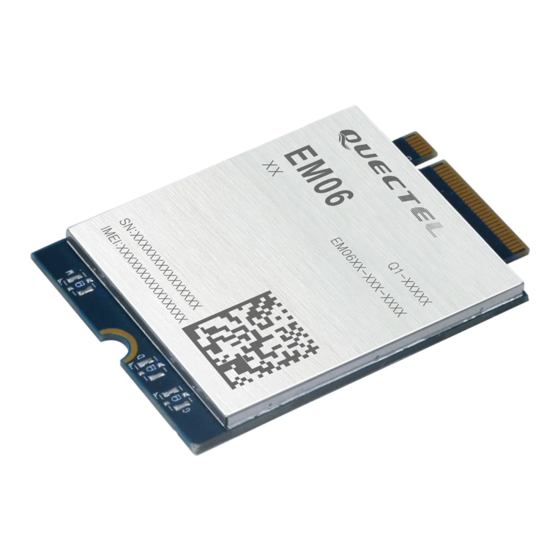
Figure 34: Top View of the Module Figure 35: Bottom View of the Module NOTE Images above are for illustration purpose only and may differ from the actual module. For authentic appearance and label, please refer to the module received from Quectel. EM06_Series_Hardware_Design 65 / 69... -
Page 67: Connector
EM06 series modules adopt standard PCI Express M.2 connectors compliant with the directives and standards listed in the document [4]. 7.5. Packaging EM06 series modules are packaged in trays. Each tray contains 10 modules. The smallest package contains 100 modules. EM06_Series_Hardware_Design... -
Page 68: Appendix References
LTE-A Module Series EM06 Series Hardware Design Appendix References Table 39: Related Documents Document Name Remark Quectel_M.2_EVB_User_Guide M.2 EVB User Guide EP06, EG06 and EM06 AT Quectel_EP06&EG06&EM06_AT_Commands_Manual Commands Manual Quectel_EP06&EG06&EM06_GNSS_AT_Commands_ EP06, EG06 and EM06 GNSS AT Manual Commands Manual PCI Express M.2 Specification PCI Express M.2 Specification... - Page 69 LTE-A Module Series EM06 Series Hardware Design Global Positioning System Global System for Mobile Communications Half Rate HSDPA High-Speed Downlink Packet Access HSPA High Speed Packet Access HSUPA High Speed Uplink Packet Access kbps kilobits per second Light Emitting Diode...
- Page 70 LTE-A Module Series EM06 Series Hardware Design Uplink UMTS Universal Mobile Telecommunications Service Unsolicited Result Code (U)SIM (Universal) Subscriber Identity Module WCDMA Wideband Code Division Multiple Access EM06_Series_Hardware_Design 69 / 69...
Need help?
Do you have a question about the EM06 Series and is the answer not in the manual?
Questions and answers