
Related Manuals for Quectel EM12-G


Summary of Contents for Quectel EM12-G
- Page 1 EM12-G Hardware Design LTE-A Module Series Rev. EM12_Hardware_Design_ Date: 2018-09-28 Status: Preliminary www.quectel.com...
- Page 2 QUECTEL OFFERS THE INFORMATION AS A SERVICE TO ITS CUSTOMERS. THE INFORMATION PROVIDED IS BASED UPON CUSTOMERS’ REQUIREMENTS. QUECTEL MAKES EVERY EFFORT TO ENSURE THE QUALITY OF THE INFORMATION IT MAKES AVAILABLE. QUECTEL DOES NOT MAKE ANY WARRANTY AS TO THE INFORMATION CONTAINED HEREIN, AND DOES NOT ACCEPT ANY LIABILITY FOR ANY INJURY, LOSS OR DAMAGE OF ANY KIND INCURRED BY USE OF OR RELIANCE UPON THE INFORMATION.
-
Page 3: About The Document
LTE-A Module Series EM12-G Hardware Design About the Document History Revision Date Author Description Oscar LIU/ Draft 2018-09-28 Initial Reed Wang EM12-G_Hardware_Design 2 / 62... -
Page 4: Table Of Contents
LTE-A Module Series EM12-G Hardware Design Contents About the Document ........................... 2 Contents ............................... 3 Table Index ..............................5 Figure Index ..............................6 Introduction ............................7 1.1. Safety Information ........................10 Product Concept ..........................11 2.1. General Description ........................11 2.2. - Page 5 LTE-A Module Series EM12-G Hardware Design Antenna Interfaces ..........................43 5.1. Main/Rx-diversity Antenna Interfaces ..................43 5.1.1. Operating Frequency ..................... 44 5.2. GNSS Antenna Interface ......................45 5.3. Antenna Installation ........................46 5.3.1. Antenna Requirements ....................46 5.3.2. Recommended RF Connector for Antenna Installation ..........46 Electrical, Reliability and Radio Characteristics ................
- Page 6 LTE-A Module Series EM12-G Hardware Design Table Index TABLE 1: FREQUENCY BANDS AND GNSS TYPE OF EM12 MODULE ............11 TABLE 2: KEY FEATURES OF EM12 ....................... 13 TABLE 3: DEFINITION OF I/O PARAMETERS ....................18 TABLE 4: PIN DESCRIPTION ........................... 18 TABLE 5: DEFINITION OF VCC AND GND PINS.....................
- Page 7 LTE-A Module Series EM12-G Hardware Design Figure Index FIGURE 1: FUNCTIONAL DIAGRAM ....................... 15 FIGURE 2: PIN ASSIGNMENT ......................... 17 FIGURE 3: POWER SUPPLY LIMITS DURING RADIO TRANSMISSION ............23 FIGURE 4: REFERENCE CIRCUIT OF VCC ....................23 FIGURE 5: REFERENCE DESIGN OF POWER SUPPLY ................24 FIGURE 6: TURN ON THE MODULE THROUGH GPIO CONTROLLED FULL_CARD_POWER_OFF# ..
-
Page 8: Introduction
減少電磁波影響,請妥適使用. The device could be used with a separation distance of 20cm to the human body. Hereby, [Quectel Wireless Solutions Co., Ltd.] declares that the radio equipment type [EM12-G] is in compliance with Directive 2014/53/EU. The full text of the EU declaration of conformity is available at the following internet address: http://www.quectel.com... - Page 9 LTE-A Module Series EM12-G Hardware Design encouraged to try to correct the interference by one or more of the following measures: -Reorient or relocate the receiving antenna. -Increase the separation between the equipment and receiver. -Connect the equipment into an outlet on a circuit different from that to which the receiver is connected.
- Page 10 LTE-A Module Series EM12-G Hardware Design fré quences radio de la CNR-102, la proximité humaine à l'antenne ne doit pas être inférieure à 20 cm (8 pouces) pendant le fonctionnement normal. IMPORTANT NOTE: This module is intended for OEM integrator. The OEM integrator is still responsible for the FCC compliance requirement of the end product, which integrates this module.
-
Page 11: Safety Information
The following safety precautions must be observed during all phases of the operation, such as usage, service or repair of any cellular terminal or mobile incorporating EM12-G module. Manufacturers of the cellular terminal should send the following safety information to users and operating personnel, and incorporate these guidelines into all manuals supplied with the product. -
Page 12: Product Concept
LTE-FDD, LTE-TDD, DC-HSDPA, HSPA+, HSDPA, HSUPA and WCDMA networks with standard PCI Express M.2 interface. EM12-G supports embedded operating systems such as Windows CE, Linux and Android, and also provides GNSS1) and voice functionality2) to meet customers’ specific application demands. - Page 13 GPS, GLONASS, BeiDou, Galileo NOTES GNSS function is optional. EM12-G contains Telematics version and Data-only version. Telematics version supports voice and data functions, while Data-only version only supports data function. B21 band follow up will be developed EM12-G can be applied in the following fields: ...
-
Page 14: Key Features
Smart Metering System Wireless Router and Switch Other Wireless Terminal Devices 2.2. Key Features The following table describes the detailed features of EM12-G. Table 2: Key Features of EM12-G Feature Details Function Interface PCI Express M.2 Interface Supply voltage: 3.135V~4.4V Power Supply Typical supply voltage: 3.7V... - Page 15 Rx-diversity Support LTE/WCDMA Rx-diversity Gen 9HT Lite of Qualcomm GNSS Features Protocol: NMEA 0183 Compliant with 3GPP TS 27.007, 27.005 and Quectel enhanced AT AT Commands commands Size: (42.0± 0.15)mm × (30.0± 0.15)mm × (2.3± 0.1)mm Physical Characteristics Weight: TBD Operation temperature range: -30°...
-
Page 16: Functional Diagram
Figure 1: Functional Diagram 2.4. Evaluation Board In order to help customers develop applications conveniently with EM12-G, Quectel supplies the evaluation board (M.2 EVB), USB to RS-232 converter cable, USB type-C cable, earphone, antenna and other peripherals to control or test the module. For more details, please refer to document [1]. -
Page 17: Application Interfaces
LTE-A Module Series EM12-G Hardware Design Application Interfaces The physical connections and signal levels of EM12-G comply with PCI Express M.2 specifications. This chapter mainly describes the definition and application of the following interfaces/signals/pins of EM12-G: Power supply ... -
Page 18: Pin Assignment
LTE-A Module Series EM12-G Hardware Design 3.1. Pin Assignment The following figure shows the pin assignment of EM12-G. The top side contains EM12-G module and antenna connectors. P in N a m e N o . N o . P in N a m e... -
Page 19: Pin Description
LTE-A Module Series EM12-G Hardware Design 3.2. Pin Description The following tables show the pin definition and description of EM12-G on the 75-pin application. Table 3: Definition of I/O Parameters Type Description Bidirectional Digital input Digital output Open drain Power input... - Page 20 PCM_CLK (AUDIO_0) slave mode, it is an input signal. domain If unused, keep it open. Connected to GND internally. CONFIG_0 CONFIG_0 EM12-G is configured as WWAN-USB 3.0. GPIO_6 1.8V power PCM_IN PCM data input (AUDIO_1) domain A signal to wake up the host.
- Page 21 LTE-A Module Series EM12-G Hardware Design (AUDIO_3) signal domain USB3.0-TX- USB3.0_TX- USB 3.0 transmit data (-) 1.8V/3.0V UIM-RESET USIM1_RESET (U)SIM1 card reset power domain USB3.0-TX+ USB3.0_TX+ USB 3.0 transmit data (+) 1.8V/3.0V UIM-CLK USIM1_CLK (U)SIM1 card clock power domain Ground...
- Page 22 Pulled up SIM_DETECT USIM1_DET (U)SIM1 card insertion detection internally RESET# RESET# System reset. Active low. SUSCLK (32kHz) Connected to GND internally. CONFIG_1 CONFIG_1 EM12-G is configured as WWAN-USB 3.0. Vmin=3.135V 3.3V Power supply Vnorm=3.7V Vmax=4.4V Ground Vmin=3.135V 3.3V Power supply Vnorm=3.7V Vmax=4.4V...
-
Page 23: Power Supply
Power supply Vnorm=3.7V Vmax=4.4V Not connected internally. CONFIG_2 CONFIG_2 EM12-G is configured as WWAN-USB 3.0. NOTES Keep all NC, reserved and unused pins unconnected. “*” means under development. 3.3. Power Supply The following table shows pin definition of VCC pins and ground pins. -
Page 24: Reference Design For Power Supply
LTE-A Module Series EM12-G Hardware Design Figure 3: Power Supply Limits during Radio Transmission To decrease voltage drop, a bypass capacitor of about 220µF with low ESR (ESR=0.7Ω) should be used, and a multi-layer ceramic chip capacitor (MLCC) array should also be reserved due to its ultra-low ESR. It is recommended to use three ceramic capacitors (100nF, 33pF, 10pF) for composing the MLCC array, and place these capacitors close to VCC pins. -
Page 25: Turn On And Off Scenarios
LTE-A Module Series EM12-G Hardware Design MIC29302WU LDO_IN 100K 1% 100nF 470uF 33pF 10pF 470R 470uF 100nF 51K 1% 4.7K MCU_POWER _ON/OFF Figure 5: Reference Design of Power Supply NOTE In order to avoid damages to the internal flash, please do not switch off the power supply directly when the module is working. -
Page 26: Turn On The Module Through Gpio Controlled Full_Card_Power_Off
LTE-A Module Series EM12-G Hardware Design 3.4.1.1. Turn on the Module Through GPIO Controlled FULL_CARD_POWER_OFF# It is recommended to use a GPIO from host to control FULL_CARD_POWER_OFF#. A simple reference circuit is illustrated in the following figure. Figure 6: Turn on the Module Through GPIO Controlled FULL_CARD_POWER_OFF# 3.4.1.2. -
Page 27: Turn Off The Module
LTE-A Module Series EM12-G Hardware Design The turn on scenario is illustrated in the following figure. NOTE RESET# ≥1.19V FULL_CARD_POWER_OFF# ≤0.2V ≥12.5s Module Status Booting Active Figure 8: Timing of Turning on Module NOTE Please make sure that VCC is stable before pulling down FUL_CARD_POWER_OFF# pin. The time between them is no less than 30ms. -
Page 28: Turn Off The Module Via At Command
LTE-A Module Series EM12-G Hardware Design 3.4.2.2. Turn off the Module via AT Command The module can also be turned off by AT+QPOWD command. For more details about the command, please refer to document [2]. 3.5. Reset the Module The RESET# pin is used to reset the module. The module can be reset by driving RESET# to a low level voltage for 250ms~600ms. -
Page 29: U)Sim Interfaces
LTE-A Module Series EM12-G Hardware Design Figure 11: Reference Circuit of RESET# by Using Button The reset scenario is illustrated in the following figure. Figure 12: Timing of Resetting Module NOTE Please ensure that there is no large capacitance on RESET# pin. - Page 30 When (U)SIM2 card is absent, it is at low level. EM12-G supports (U)SIM card hot-plug via the USIM_DET pin, which is a level trigger pin. The USIM_DET is normally short-circuited to ground when (U)SIM card is not inserted. When the (U)SIM card is inserted, the USIM_DET will change from low to high level.
- Page 31 LTE-A Module Series EM12-G Hardware Design USIM_VDD 100nF (U)SIM Card Connector USIM_VDD USIM_RESET Module USIM_CLK USIM_DET USIM_DATA 33pF 33pF 33pF Figure 13: Reference Circuit of Normally Short-Circuited (U)SIM Card Connector Normally Short-Circuited (U)SIM Card Connector: When the (U)SIM is absent, CD is short-circuited to SW and USIM_DET is at low level.
- Page 32 LTE-A Module Series EM12-G Hardware Design If (U)SIM card detection function is not needed, please keep USIM_DET unconnected. A reference circuit for (U)SIM card interface with a 6-pin (U)SIM card connector is illustrated in the following figure. USIM_VDD 100nF USIM_GND...
-
Page 33: Usb Interface
EM12-G Hardware Design 3.7. USB Interface EM12-G provides one integrated Universal Serial Bus (USB) interface which complies with the USB 3.0/2.0 specifications and supports super speed (5Gbps) on USB 3.0, high speed (480 Mbps) and full speed (12 Mbps) modes on USB 2.0. The USB interface is used for AT command communication, data transmission, GNSS NMEA output, software debugging, firmware upgrade and voice over USB*. - Page 34 LTE-A Module Series EM12-G Hardware Design Test Points Minimize these stubs NM_0R NM_0R ESD Array USB_DM USB_DM USB_DP USB_DP 100nF USB3.0_RX+ USB3.0_TX+ 100nF USB3.0_RX- USB3.0_TX- 100nF USB3.0_TX+ USB3.0_RX+ 100nF USB3.0_TX- USB3.0_RX- Module Figure 16: Reference Circuit of USB 2.0 & 3.0 Interface In order to ensure the integrity of USB 2.0 &...
-
Page 35: Pcie Interface
The PCM_SYNC rising edge represents the MSB. In this mode, PCM interface operates with a 256kHz PCM_CLK and an 8kHz, 50% duty cycle PCM_SYNC only. EM12-G supports 16-bit linear data format. The following figures show the primary mode’s timing relationship with 8kHz PCM_SYNC and 2048kHz PCM_CLK, as well as the auxiliary mode’s timing relationship with 8kHz PCM_SYNC and 256kHz PCM_CLK. - Page 36 LTE-A Module Series EM12-G Hardware Design 125us PCM_CLK PCM_SYNC PCM_OUT PCM_IN Figure 17: Primary Mode Timing 125us PCM_CLK PCM_SYNC PCM_OUT PCM_IN Figure 18: Auxiliary Mode Timing The following table shows the pin definition of PCM and I2C interfaces which can be applied on audio codec design.
-
Page 37: Control And Indicator Signals
It is recommended to reserve an RC (R=22Ω, C=22pF) circuit on the PCM lines, especially for PCM_CLK. EM12-G works as a master device pertaining to I2C interface. 3.10. Control and Indicator Signals The following table shows the pin definition of control and indicator signals. -
Page 38: W_Disable1# Signal
“*” means under development. 3.10.1. W_DISABLE1# Signal EM12-G provides a W_DISABLE1# signal to disable or enable airplane mode through hardware operation. The W_DISABLE1# pin is pulled up by default. Driving it to low level will let the module enter into airplane mode. -
Page 39: Wwan_Led# Signal
LTE-A Module Series EM12-G Hardware Design 3.10.2. WWAN_LED# Signal The WWAN_LED# signal is used to indicate the RF status of the module, and its typical current consumption is up to 40mA. In order to reduce the current consumption of the LED, a resistor must be placed in series with the LED, as illustrated in the figure below. -
Page 40: Dpr Signal
EM12-G provides a DPR (Dynamic Power Reduction) signal for body SAR (Specific Absorption Rate) detection. The signal is sent by a host system proximity sensor to EM12-G module to provide an input trigger which will reduce the output power in the radio transmission. -
Page 41: Tunable Antenna Control Interface
Tunable antenna control 1.8V power domain NOTE “*” means under development. 3.12. Configuration Pins EM12-G provides 4 configuration pins, and it is configured as WWAN-USB 3.0 2. Table 17: Pin Definition of Configuration Pins Pin No. Pin Name Power Domain... - Page 42 LTE-A Module Series EM12-G Hardware Design Table 18: List of Configuration Pins Config_0 Config_1 Config_2 Config_3 Module Type and Port (Pin 21) (Pin 69) (Pin 75) (Pin 1) Main Host Interface Configuration WWAN-USB 3.0 EM12-G_Hardware_Design 41 / 62...
-
Page 43: Gnss Receiver
EM12-G supports standard NMEA-0183 protocol, and outputs NMEA sentences at 1Hz data update rate via USB interface by default. By default, EM12-G GNSS engine is switched off. It has to be switched on via AT command. For more details about GNSS engine technology and configurations, please refer to document [3]. -
Page 44: Antenna Interfaces
EM12-G Hardware Design Antenna Interfaces EM12-G provides a main antenna interface, an Rx-diversity antenna interface which is used to resist the fall of signals caused by high speed movement and multipath effect, and a GNSS antenna interface. The antenna ports have an impedance of 50Ω. -
Page 45: Operating Frequency
LTE-A Module Series EM12-G Hardware Design 5.1.1. Operating Frequency Table 19: EM12-G Operating Frequencies 3GPP Band Transmit Receive Unit WCDMA B1 1920~1980 2110~2170 WCDMA B2 1850~1910 1930~1990 WCDMA B3 1710~1785 1805~1880 WCDMA B4 1710~1755 2110~2155 WCDMA B5 824~849 869~894 WCDMA B8... -
Page 46: Gnss Antenna Interface
LTE-A Module Series EM12-G Hardware Design LTE B20 832~862 791~821 LTE B21 1447.9~1462.9 1495.9~1510.9 LTE B25 1850~1915 1930~1995 LTE B26 814~849 859~894 LTE B28 703~748 758~803 LTE B29 717~728 LTE B30 2305~2315 2350~2360 LTE B32 1452~1496 LTE B38 2570~2620 2570~2620... -
Page 47: Antenna Installation
GNSS performance. 5.3.2. Recommended RF Connector for Antenna Installation EM12-G is mounted with standard 2mm × 2mm receptacle RF connectors for convenient antenna connection. The connector dimensions are illustrated below: EM12-G_Hardware_Design... - Page 48 Max 1.3 (DC~3GHz) Max 1.45 (3GHz~6GHz) The receptacle RF connector used in conjunction with EM12-G will accept two types of mating plugs that will meet a maximum height of 1.2mm using a Ø0.81mm coaxial cable or a maximum height of 1.45mm utilizing a Ø1.13mm coaxial cable.
- Page 49 EM12-G Hardware Design Figure 25: Specifications of Mating Plugs Using Ø0.81mm Coaxial Cables The following figure illustrates the connection between the receptacle RF connector on EM12-G and the mating plug using a Ø0.81mm coaxial cable. Figure 26: Connection between RF Connector and Mating Plug Using Ø0.81mm Coaxial Cable The following figure illustrates the connection between the receptacle RF connector on EM12-G and the mating plug using a Ø1.13mm coaxial cable.
- Page 50 LTE-A Module Series EM12-G Hardware Design Figure 27: Connection between RF Connector and Mating Plug Using Ø1.13mm Coaxial Cable EM12-G_Hardware_Design 49 / 62...
-
Page 51: Electrical, Reliability And Radio Characteristics
Voltage at Digital Pins -0.3 6.2. Power Supply Requirements The typical input voltage of EM12-G is 3.7V, as specified by PCIe M.2 Electromechanical Spec Rev1.0. The following table shows the power supply requirements of EM12-G. Table 24: Power Supply Requirements... -
Page 52: I/O Requirements
LTE-A Module Series EM12-G Hardware Design 6.3. I/O Requirements Table 25: I/O Requirements Parameter Description Min. Max. Unit Input high voltage 0.7 × V +0.3 DD18 DD18 Input low voltage -0.3 0.3 × V DD18 Output high voltage -0.5 DD18... -
Page 53: Current Consumption(Tbd)
LTE-A Module Series EM12-G Hardware Design 6.5. Current Consumption(TBD) 6.6. RF Output Power The following table shows the RF output power of EM12-G module. Table 27: RF Output Power Frequency Max. Min. WCDMA bands 24dBm+1/-3dB <-50dBm LTE- FDD bands 23dBm± 2dB <-40dBm... - Page 54 LTE-A Module Series EM12-G Hardware Design LTE-FDD B2 (10M) -97.5 -97.0 -99.5dbm -94.3dBm LTE-FDD B3 (10M) -97.0 -96.5 -99.0dbm -93.3dBm LTE-FDD B4 (10M) -97.0 -96.0 -99.0dBm -96.3dBm LTE-FDD B5 (10M) -98.5 -98.5 -100.5dBm -94.3dBm LTE-FDD B7 (10M) -96.5 -96.0 -98.5dBm -94.3dBm...
-
Page 55: Esd Characteristics
± 1 6.9. Thermal Dissipation EM12-G is designed to work over an extended temperature range. In order to achieve a maximum performance while working under extended temperatures or extreme conditions (such as with maximum power or data rate, etc.) for a long time, it is strongly recommended to add a thermal pad or other thermally conductive compounds between the module and the main PCB for thermal dissipation. - Page 56 LTE-A Module Series EM12-G Hardware Design Figure 28: Thermal Dissipation Area on Bottom Side of Module (Top View) There are some other measures to enhance heat dissipation performance: Add ground vias as many as possible on PCB. Maximize airflow over/around the module.
-
Page 57: Mechanical Dimensions And Packaging
EM12-G Hardware Design Mechanical Dimensions and Packaging This chapter mainly describes mechanical dimensions and packaging specifications of EM12-G module. All dimensions are measured in mm, and the tolerances for dimensions without tolerance values are ± 0.05mm. 7.1. Mechanical Dimensions of the Module... -
Page 58: Standard Dimensions Of M.2 Pci Express
A and B. Figure 30: Standard Dimensions of M.2 Type 3042-S3 (Unit: mm) According to M.2 nomenclature, EM12-G is Type 3042-S3-B (30.0mm × 42.0mm, max component height on the top is 1.5mm and single-sided, key ID is B). -
Page 59: Design Effect Drawings Of The Module
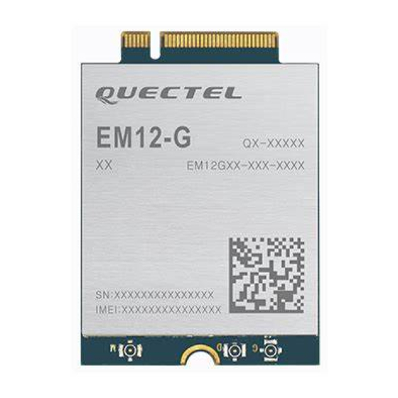
7.3. Design Effect Drawings of the Module Figure 32: Top View of the Module NOTE These are design effect drawings of EM12-G module. For more accurate pictures, please refer to the module that you get from Quectel. 7.4. M.2 Connector EM12-G adopts a standard PCI Express M.2 connector which compiles with the directives and standards... -
Page 60: Packaging
Meanwhile, the SN and IMEI can be checked by scanning the QR code. 7.6. Packaging EM12-G modules are packaged in trays. The following figure shows the tray size. Figure 33: Tray Size Each tray contains 10 modules. The smallest package contains 100 modules. Tray packaging procedure as below. - Page 61 LTE-A Module Series EM12-G Hardware Design Figure 34: Tray Packaging Procedure EM12-G_Hardware_Design 60 / 62...
-
Page 62: Appendix References
LTE-A Module Series EM12-G Hardware Design Appendix References Table 30: Related Documents Document Name Remark Quectel_M.2_EVB_User_Guide M.2 EVB User Guide EP06, EG06 and EM06 AT Quectel_EP06&EG06&EM06_AT_Commands_Manual Commands Manual Quectel_EP06&EG06&EM06_GNSS_AT_Commands_ EP06, EG06 and EM06 GNSS AT Manual Commands Manual PCI Express M.2 Specification... - Page 63 LTE-A Module Series EM12-G Hardware Design HSUPA High Speed Uplink Packet Access kbps Kilo Bits Per Second Light Emitting Diode Long Term Evolution Mbps Million Bits Per Second Mobile Equipment (Module) MIMO Multiple-Input Multiple-Output MLCC Multiplayer Ceramic Chip Capacitor Multimedia Messaging Service...
Need help?
Do you have a question about the EM12-G and is the answer not in the manual?
Questions and answers