
Related Manuals for Cypress WICED CYW920706WCDEVAL


Summary of Contents for Cypress WICED CYW920706WCDEVAL
- Page 1 CYW920706WCDEVAL Hardware User Guide Associated Part Family: CYW20706 Doc. No.: 002-16535 Rev. ** Cypress Semiconductor 198 Champion Court San Jose, CA 95134-1709 www.cypress.com Arrow.com. Downloaded from...
-
Page 2: Table Of Contents
Contents About This Document ................................4 Purpose and Audience ..............................4 Scope ....................................4 Acronyms and Abbreviations ............................4 IoT Resources and Technical Support ..........................4 Product Description ..............................5 Board Layout.................................. 7 Board Block Diagram ..............................8 Jumper and DIP Switch Settings ..........................9 Current Consumption Measurement .......................... - Page 3 References .................................... 46 Document Revision History ..............................47 Worldwide Sales and Design Support ..........................48 Products ..................................48 PSoC® Solutions ................................48 Cypress Developer Community ............................. 48 Technical Support ................................48 CYW920706WCDEVAL Hardware User Guide Doc. No.: 002-16535 Rev. ** Arrow.com.
-
Page 4: About This Document
IoT device for your design, and quickly and effectively integrate the device into your design. Cypress provides customer access to a wide range of information, including technical documentation, schematic diagrams, product bill of materials, PCB layout information, and software updates. -
Page 5: Product Description
Cortex™-M3 processor and an integrated transceiver. It is a fully embedded device running an embedded BT stack with support for embedded user applications developed with WICED Studio. The Cypress CYW920706WCDEVAL board (Figure 1-1) is an evaluation board that provides various pins, jumpers, switches, ports, and test points to access CYW20706 to perform debug, evaluation, and troubleshooting. - Page 6 0BProduct Description Figure 1-2 shows the pins connected to the user accessible headers on the board. Figure 1-2. User Accessible headers CYW920706WCDEVAL Hardware User Guide Doc. No.: 002-16535 Rev. ** Arrow.com. Arrow.com. Arrow.com. Arrow.com. Arrow.com. Arrow.com. Downloaded from Downloaded from Downloaded from Downloaded from Downloaded from...
-
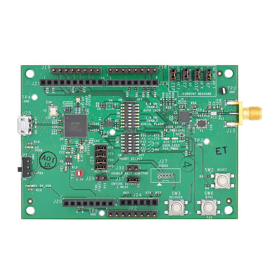
Page 7: Board Layout
2 Board Layout Figure 2-1 shows the location of key jumpers and switches on the CYW920706WCDEVAL board. Figure 2-1. CYW920706WCDEVAL Evaluation Board Layout and Component Locations Note: Jumpers which are shorted by default are identified in red. CYW920706WCDEVAL Hardware User Guide Doc. -
Page 8: Board Block Diagram
3 Board Block Diagram Figure 3-1 shows the block diagram of CYW20706 connections on the CYW920706WCDEVAL board. Figure 3-1 Board Block Diagram CYW920706WCDEVAL Hardware User Guide Doc. No.: 002-16535 Rev. ** Arrow.com. Arrow.com. Arrow.com. Arrow.com. Arrow.com. Arrow.com. Arrow.com. Arrow.com. Downloaded from Downloaded from Downloaded from Downloaded from... -
Page 9: Jumper And Dip Switch Settings
4 Jumper and DIP Switch Settings Figure 2-1 shows the location for SW5, a switch that is used to configure Peripheral UART (PUART). Settings are shown in Table 4-1. Default State Description Set this switch ON to use P2 as PUART_RX Set this switch ON to use P33 as PUART_RX Set this switch ON to use P0 as PUART_TX Set this switch ON to use P31 as PUART_TX... - Page 10 Jumper and DIP Switch Settings Jumper/Switch Default State Comment Shorted Short this Jumper to supply 3.3V to the IO Domain (VDDIO) of the 0270x. Also use this jumper to measure the current consumption of the IO Domain. Shorted Input of the internal 1.2V LDO, use this jumper to measure current consumption at the input of the 1.2V LDO Shorted Input of the internal 2.5V LDO, use this jumper to measure current consumption at the input of the...
-
Page 11: Current Consumption Measurement
5 Current Consumption Measurement Table 5-1 shows the low-power Bluetooth classic mode current measured for different sleep modes in three different scenarios. Mode J9 (1.2V Core + Radio) J3 (IO Domain) J9 +J3 Units No scans enabled + sleep mode 0.114 0.084 0.198... -
Page 12: Schematics
6 Schematics Figure 6-1. CYW920706WCDEVAL Baseband Schematic CYW920706WCDEVAL Hardware User Guide Doc. No.: 002-16535 Rev. ** Arrow.com. Arrow.com. Arrow.com. Arrow.com. Arrow.com. Arrow.com. Arrow.com. Arrow.com. Arrow.com. Arrow.com. Arrow.com. Arrow.com. Downloaded from Downloaded from Downloaded from Downloaded from Downloaded from Downloaded from Downloaded from Downloaded from Downloaded from... - Page 13 Figure 6-2. CYW920706WCDEVAL RF Schematic CYW920706WCDEVAL Hardware User Guide Doc. No.: 002-16535 Rev. ** Arrow.com. Arrow.com. Arrow.com. Arrow.com. Arrow.com. Arrow.com. Arrow.com. Arrow.com. Arrow.com. Arrow.com. Arrow.com. Arrow.com. Arrow.com. Downloaded from Downloaded from Downloaded from Downloaded from Downloaded from Downloaded from Downloaded from Downloaded from Downloaded from Downloaded from...
- Page 14 Figure 6-3. CYW920706WCDEVAL Power & Headers Schematic CYW920706WCDEVAL Hardware User Guide Doc. No.: 002-16535 Rev. ** Arrow.com. Arrow.com. Arrow.com. Arrow.com. Arrow.com. Arrow.com. Arrow.com. Arrow.com. Arrow.com. Arrow.com. Arrow.com. Arrow.com. Arrow.com. Arrow.com. Downloaded from Downloaded from Downloaded from Downloaded from Downloaded from Downloaded from Downloaded from Downloaded from...
- Page 15 Figure 6-4. CYW920706WCDEVAL USB to UART Interface Schematic CYW920706WCDEVAL Hardware User Guide Doc. No.: 002-16535 Rev. ** Arrow.com. Arrow.com. Arrow.com. Arrow.com. Arrow.com. Arrow.com. Arrow.com. Arrow.com. Arrow.com. Arrow.com. Arrow.com. Arrow.com. Arrow.com. Arrow.com. Arrow.com. Downloaded from Downloaded from Downloaded from Downloaded from Downloaded from Downloaded from Downloaded from...
-
Page 16: Cyw20706 Interfaces
7 CYW20706 Interfaces The package CYW20706 is available in may have fewer GPIOs than the die. Some of these GPIOs are fixed function IOs while others are reconfigurable for different interfaces. To accommodate its various applications, interface selection is accomplished through a combination of signal routing to CYW20706 and programming using the WICED API described in later sections. -
Page 17: Selectable Interfaces
6BCYW20706 Interfaces Selectable Interfaces CYW20706 supports several other interfaces besides those identified in Fixed Interfaces. Although CYW20706 supports several other interfaces, it cannot support all of its interfaces in a single hardware board design. Therefore, board designers must select which interfaces to use in a given design. The key limitation on the selectable interfaces is the number of available digital I/O pins. - Page 18 Table 7-2 shows which of the selectable CYW20706 interfaces are supported on the CYW920706WCDEVAL board. Description CYW20706 Bonded Schematic Signal Name Default GPIOs I/O Type Signal Function and Notes State I2S_PCM_OUT/P3/P29/P35 I2S_PCM_OUT I2S_DO/PCM_OUT. To use I S, set SW5-5 to the OFF position, fr the pcm_config structure pointer with the mode role set and use th wiced_hal_set_pcm_config to select the I S function.
- Page 19 Description CYW20706 Bonded Schematic Signal Name GPIOs Default I/O Type Signal Function and Notes State Floating I/O No specific function defined. It can be monitored at J22-5 if the I I/Os P2 and P28 are disabled. This pin can be configured as I wiced_hal_i2c_init(WICED_I2C_SDA_P35_SCL_P37) which sele BT_GPIO_3/P27/P33 BT_GPIO_3...
- Page 20 Description CYW20706 Bonded Schematic Signal Name GPIOs Default I/O Type Signal Function and Notes State Floating I (master) SPI1_MISO (master or slave). To use, disable I/O P32. O (slave) Floating I/O No specific function defined. It can be monitored at J19-4 if I/O P2 BT_DEV_WAKE/P36/P38 BT_DEV_WAKE A signal from the host to CYW20706 that the host requires attentio...
-
Page 21: Gpio Information
8 GPIO Information 8.1 GPIO_Pxx The Cypress WICED Studio API provides configuration support for up to 40 multiplexed GPIOs (represented as WICED_GPIO_P0 through WICED_GPIO_P39). CYW20706 uses 23 of these multiplexed GPIOs. The assignment of the multiplexed GPIOs to physical device pins is restricted from certain digital I/O pins when certain interfaces or signal functional are used. -
Page 22: Multiplexed Gpio_Pxx Interface Summary
8.1.1 Multiplexed GPIO_Pxx Interface Summary Table 8-2 provides an interface summary of the 23 multiplexed GPIOs used by CYW20706. The description column provides the potential signal functions of each GPIO and the associated I/O type of each signal function. Description CYW20706 Pin GPIO I/O Type... - Page 23 7BGPIO Information Description CYW20706 Pin GPIO I/O Type Signal Function Options General purpose, user-defined GPIO X-coordinate output from a quadrature detector (QDX0) Peripheral UART RX input (PUART_RX) SPI1_CS (slave) SPI1_MOSI (master) General purpose, user-defined GPIO Optical control output (QOC2) A/D converter input (A/D input 11) PWM output (PWM2) General purpose, user-defined GPIO A/D converter input (A/D input 2)
- Page 24 7BGPIO Information Description CYW20706 Pin GPIO I/O Type Signal Function Options A/D converter input (A/D input 23) BSC SCL (I2C_SCL) General purpose, user-defined GPIO A/D converter input (A/D input 29) Peripheral UART TX output (PUART_TX) SPI1_MOSI (master output) SPI1_MOSI (slave input) Infrared learning input (IR_RX) 60 Hz input (60Hz_main) to a zero-crossing detector.
-
Page 25: Digital I/O Pin Interface Mapping
7BGPIO Information Description CYW20706 Pin GPIO I/O Type Signal Function Options Peripheral UART TX output (PUART_TX) General purpose, user-defined GPIO A/D converter input (A/D input 3) Z-coordinate output from a quadrature detector (QDZ0) SPI1_CLK (master) SPI1_CLK (slave) Auxiliary clock output (ACLK0) T/R switch control (~TX_PD) General purpose, user-defined GPIO A/D converter input (A/D input 1) - Page 26 7BGPIO Information • GPIO_P6 (a general-purpose user-defined I/O) • GPIO_P31 (a general-purpose user-defined I/O) • PUART_TX (a peripheral UART TX output multiplexed to GPIO_P31) • PUART_RTS (a peripheral UART request-to-send output multiplexed to GPIO_P6) • SPI1_CS (a SPI interface chip-select input multiplexed to GPIO_P6) •...
- Page 27 J22.8/ J23.6/ J21.2 J22.3/ J24.1 J22.4/ J23.5 J22.5 J19.5/ J21.7 J19.2/ J23.4 J22.7/ J23.5/ J21.1 J22.6/ J23.6 P34 P34 J19.1 J19.4/ J21.6 J19.6/ J21.8 J19.3/ J21.5 Table 8-3. Interface Mapping to the 12 Available Digital I/O Pins * This instance of P2 is SPI1_MOSI (master only). An X in the red rectangle indicates that the associated signal functions do not involve any LHL GPIO signals.
-
Page 28: Lhl Gpio Capabilities
7BGPIO Information 8.2 LHL GPIO Capabilities The LHL GPIOs have the following capabilities: Each can be programmed to serve one of the signal functions associated with it (see Multiplexed GPIO_Pxx Interface Summary Table 8-2). All can be input and output disabled (HI-Z), input enabled, or output enabled. ... -
Page 29: Interface Signal Function Selection Restrictions And Considerations
9 Interface Signal Function Selection Restrictions and Considerations This section provides signal-function selection restrictions and/or general information associated with the following CYW20706 interfaces: I2S and PCM SPI1 SPI2 HCI UART Peripheral UART Broadcom Serial Control (BSC) (Compatible with I2C) ... -
Page 30: Spi1
Interface Signal Function Selection Restrictions and Considerations 9.2.1 SPI1 The application has full control of the SPI1 interface. The SPI1 interface supports: SPI clock modes 0 through 4. A maximum transaction size of 254 bytes. A maximum clock speed of 12 MHz for all I/O supply levels. Note: Running the SPI clock at speeds above 12 MHz can lead to undesired behavior. -
Page 31: Spi1 Slave
Interface Signal Function Selection Restrictions and Considerations 9.2.1.2 SPI1 Slave Table 9-3 shows CYW20706 SPI1 slave bus-configuration options. SPI1_CLK SPI1_MOSI SPI1_MISO Option LHL GPIO Pxx LHL GPIO Pxx LHL GPIO Pxx Table 9-3. CYW20706 SPI1 Slave Bus-Configuration Options Note: The bus signals of a peripheral UART (PUART) has certain restrictions if included in a system design that also uses the SPI1 interface. -
Page 32: Swd Debugging With The Hci Uart
Interface Signal Function Selection Restrictions and Considerations In CYW20706, it is available only for application-defined HCI commands and events; it is not for Bluetooth standard HCI commands. In CYW20706, it is used to communicate with the external MCU and does support Bluetooth standard HCI commands. - Page 33 Interface Signal Function Selection Restrictions and Considerations PUART_RX PUART_TX PUART_RTS PUART_CTS Option LHL GPIO LHL GPIO LHL GPIO LHL GPIO Pxx CYW920706WCDEVAL Hardware User Guide Doc. No.: 002-16535 Rev. ** Arrow.com. Arrow.com. Arrow.com. Arrow.com. Arrow.com. Arrow.com. Arrow.com. Arrow.com. Arrow.com. Arrow.com. Arrow.com.
-
Page 34: Broadcom Serial Control (Bsc)
2 is used. So the remaining PUART bus-configuration options become 1–6, 15, and 16. 9.5 Broadcom Serial Control (BSC) (Compatible with I CYW20706 supports a Broadcom Serial Control (BSC) interface. Note: BSC is a proprietary Cypress interface that is compatible with I The following information applies to the BSC interface: ... -
Page 35: Nvram
Interface Signal Function Selection Restrictions and Considerations For a BSC programming example, see Section 10.4 “BSC Programming Example”. 9.6 NVRAM CYW20706 has NVRAM, which can be used to save the state of the device while power is off. For example, an application can use the NVRAM to save the Bluetooth Device address of a paired device. During a future connection establishment, the application can check whether the connecting device is paired or not. -
Page 36: Interface Programming Information And Examples
10 Interface Programming Information and Examples Note: All code and code references in this section pertain to WICED Studio. Source C files may be found under the appropriate application folder in the Project Explorer window under 20706-A2_Bluetooth\apps, and header H files which contain definitions for the #define’s used in the example code may be found under 20706-A2_Bluetooth\include. - Page 37 Interface Programming Information and Examples WICED_BT_TRACE( "sample_gpio_app_management_cback %d\n\r", event ); switch( event ) /* Bluetooth stack enabled */ case BTM_ENABLED_EVT: /* Initializes the GPIO driver */ wiced_hal_mia_init( ); wiced_hal_gpio_init( ); wiced_hal_mia_enable_mia_interrupt( TRUE ); wiced_hal_mia_enable_lhl_interrupt( TRUE ); /* Sample function configures LED pin as output * sends a square wave on it * if testing pin 31 then disable puart*/ gpio_test_led( );...
-
Page 38: Spi1 Master Programming Example
Interface Programming Information and Examples wiced_hal_gpio_register_pin_for_interrupt( WICED_GPIO_BUTTON, gpio_interrrupt_handler, NULL ); /* Get the pin configuration set above */ pin_config = wiced_hal_gpio_get_pin_config( WICED_GPIO_BUTTON ); WICED_BT_TRACE( "Pin config of P%d is %d\n\r", WICED_GPIO_BUTTON, pin_config ); /* The function invoked on timeout of app seconds timer. */ void seconds_app_timer_cb( uint32_t arg ) wiced_timer_count++;... -
Page 39: Spi1 Slave Programming Example
Interface Programming Information and Examples wiced_hal_pspi_init( MASTER, GPIO_PULL_UP, MASTER1_P24_CLK_P27_MOSI_P25_MISO, SPIFFY_SPEED, SPI_MSB_FIRST, SPI_SS_ACTIVE_LOW, SPI_MODE_3, WICED_GPIO_33 ); /* Send a byte and receive a byte from slave*/ test_spiffy1_master_send_receive_byte( 1 ); /* Sends one byte and receives one byte from the SPI slave. * byteToSend - The byte to send to the slave. -
Page 40: Bsc Programming Example
Interface Programming Information and Examples uint8_t test_spiffy1_slave_send_receive_byte( void ) uint8_t byteReceived; /* Rx one byte of data */ wiced_hal_pspi_rx_data( 1, &byteReceived ); /* Send back byteReceived + 1 */ byteReceived++; /* Tx one byte of data */ wiced_hal_pspi_tx_data( 1, &byteReceived ); 10.4 BSC Programming Example The following example shows how to initialize the BSC as a master, and how to write, read, and use the combination write- then-read transactions. -
Page 41: Puart Programming Example
Interface Programming Information and Examples 10.5 PUART Programming Example The following example shows how to initialize the peripheral UART. The complete working project for this example can be found in WICED Studio under Project Explorer 20706-A2_Bluetooth\apps\snip\hal_puart. Pertinent sections of source file hal_puart_app.c are shown here: #include "wiced_hal_puart.h"... -
Page 42: Nvram Programming Example
Interface Programming Information and Examples 10.6 NVRAM Programming Example The following code sample provides an example of writing a Bluetooth device address to NVRAM and reading it back. #define APP_VS_ID WICED_NVRAM_VSID_START BD_ADDR bd_addr_write = { 0x01, 0x02, 0x03, 0x04, 0x05, 0x06}; BD_ADDR bd_addr_read;... -
Page 43: Appendix A. Power-Save Options
Appendix A. Power-Save Options The WICED Studio API provides two power-save options for CYW20706, each initiated by a function call. The power-save options are: Low Power Sleep Mode – reduced power consumption, device configured to sleep when idle, application is suspended. ... - Page 44 Power-Save Options Applications can register callback functions to be notified of deep sleep transition attempts, possible transition aborts, and to allow or disallow the actual transition to deep sleep: wiced_power_save_register_approve_cback – register callback to approve or disapprove transition The callback registered with this function is called when the device has decided to transition to deep sleep, to allow an application to approve or disapprove of CYW20706 transitioning to the power-save mode.
- Page 45 Power-Save Options WICED_BT_TRACE("Cancelling deep sleep mode now...\n"); wiced_power_save_stop(); else WICED_BT_TRACE("Disapproving deep sleep request for now to delay it...\n"); return 0; void power_save_enter(void) /* too late to try to stop it now, can only store state */ wiced_power_save_store_state(persistent_state_info); WICED_BT_TRACE("Entering deep sleep now...\n"); void power_save_abort(void) /* device has aborted the deep sleep, it will not retry further unless requested */ WICED_BT_TRACE("Deep Sleep request aborted.\n");...
-
Page 46: References
References Document (or Item) Name Number Source CYW20706 Embedded Bluetooth 4.2 SoC with MCU, 002-14790 community.cypress.com Bluetooth Transceiver, and Baseband Processor WICED CYW920706WCDEVAL Kit Guide 002-18191 community.cypress.com CYW920706WCDEVAL Hardware User Guide Doc. No.: 002-16535 Rev. ** Arrow.com. Arrow.com. Arrow.com. Arrow.com. -
Page 47: Document Revision History
Document Revision History Document Title: CYW920706WCDEVAL Hardware User Guide Document Number: 002-16535 Revision Issue Date Description of Change 5829476 07/26/2017 Initial release CYW920706WCDEVAL Hardware User Guide Doc. No.: 002-16535 Rev. ** Arrow.com. Arrow.com. Arrow.com. Arrow.com. Arrow.com. Arrow.com. Arrow.com. Arrow.com. Arrow.com. Arrow.com. -
Page 48: Worldwide Sales And Design Support
Cypress is not liable, in whole or in part, and you shall and hereby do release Cypress from any claim, damage, or other liability arising from or related to all Unintended Uses of Cypress products.
Need help?
Do you have a question about the WICED CYW920706WCDEVAL and is the answer not in the manual?
Questions and answers