Table of Contents
Advertisement
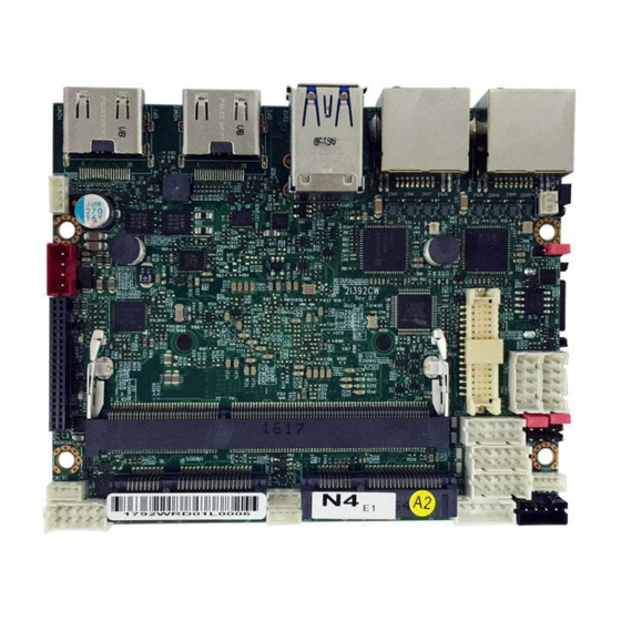
2I392CW
Intel Apollo Lake N4200 / N3350 / E3950 SoC CPU ,
DDR3L SODIMM, 2 x LAN / HDMI / USB / COM
/ PCIe mini card
All-In-One eIO extension SBC
Intel Apollo Lake N4200 / N3350 / E3950 SoC CPU
2 x HDMI, LVDS, 2 x mini PCIe, 2 x LAN, Audio
SATA, USB, COM, eIO, Wide Range DC-IN
NO. 2I392CW
Release date: Apr. 11. 2018
Advertisement
Table of Contents

Related Manuals for Lex System 2I392CW


Summary of Contents for Lex System 2I392CW
- Page 1 All-In-One eIO extension SBC Intel Apollo Lake N4200 / N3350 / E3950 SoC CPU 2 x HDMI, LVDS, 2 x mini PCIe, 2 x LAN, Audio SATA, USB, COM, eIO, Wide Range DC-IN NO. 2I392CW Release date: Apr. 11. 2018...
-
Page 2: Table Of Contents
CHAPTER 2 HARDWARE INSTALLATION ..............2-1 UNPACKING PRECAUTION ..................2-2 UNPACKING CHECKUP ....................2-3 DIMENSION-2I392CW ....................2-4 LAYOUT-2I392CW-CONNECTOR AND JUMPER ............2-4-1 LAYOUT-2I392CW-CONNECTOR AND JUMPER BOT ..........2-5 LAYOUT-2I392CW-FUNCTION MAPTOP ..............2-5-1 LAYOUT-2I392CW-FUNCTION MAP BOT ............... 2-6 DIAGRAM-2I392CW TOP .................... 2-6-1 DIAGRAM-2I392CW BOT .................. - Page 3 3-9 DC POWER INPUT ...................... 3-10 DC +12V/+5 VOLTAGE POWER OUTPUT ..............3-11 USB INTERFACE ....................... 3-12 DISPLAY INTERFACE ....................3-13 CPP1: PANEL INVERTER POWER (1X5 PIN 2.0MM WAFER) ......... 3-14 CT1: TOUCH SCREEN (2X5 PIN 2.0MM WAFER) USB INTERFACE ...... 3-15 SATA INTERFACE .....................
- Page 4 Copyright This manual is copyrighted and all rights are reserved. It does not allow any non authorization in copied, photocopied, translated or reproduced to any electronic or machine readable form in whole or in part without prior written consent from the manufacturer. In general, the manufacturer will not be liable for any direct, indirect, special, incidental or consequential damages arising from the use of inability to use the product or documentation, even if advised of the possibility of such damages.
-
Page 5: Warning
Warning ! Battery Batteries on board are consumables. The life time of them are not guaranteed. 2. Fless solution with HDD The specifi cation & limitation of HDD should be considered carefully when the fanless solution is implemented. We will not give further notifi cation in case of changes of product information and manual. -
Page 6: Hardware Notice Guide
Hardware Notice Guide 1. Before linking power supply with the motherboard, please attach DC-in adapter to the motherboard fi rst. Then plug the adapter power to AC outlet. Always shut down the computer normally before you move the system unit or remove the power supply from the motherboard. - Page 7 Photo 1 Insert Unplug...
-
Page 8: Chapter 1 General Information
Chapter-1 General Information The 2I392CW is a Pico-ITX SBC with LEX eIO (2 x PCIe + USB) expansion function offer the ideal & reliable platforms for high performance applications in Digital Signage, medical devices, POS / Kiosk, gaming machines, automation, military & industrial facilities. -
Page 9: Major Feature
1-1 Major Feature Mobile Intel® Pentium N4200 1.1GHz / 2.5GHz, (Quad core), Mobile Intel® Celeron N3350 1.1GHz / 2.4GHz (Dual core) Apollo-Lake Integrated Graphics chipset, Mobile Intel® Pentium N4200 200MHz / 700MHz, Mobile Intel® Celeron N3350 200MHz / 650MHz Support eDP 1.3 2 Lanes up to 1920 x 1200, DVI 1.2 1920 x 1080, HDMI 1.4b up to 3840 x 2160 DDR3L SODIMM slot x 1, up to 8GB Support 2 x 10 / 100 / 1000 Mbps Intel LAN port. -
Page 10: Specification
1-2 Specifi cation SOC: Mobile Intel® Pentium N4200 1.1GHz / 2.5GHz, (Quad core), Mobile Intel® Celeron N3350 1.1GHz / 2.4GHz (Dual core) Memory: DDR3L SODIMM slot x 1, up to 8GB Graphics: Apollo-Lake Integrated Graphics chipset, Mobile Intel® Pentium N4200 200MHz / 700MHz, Mobile Intel®... -
Page 11: Installing The So-Dimm
1-3 Installing the SO-DIMM 1. Align the SO-DIMM with the connector at a 45 degree angle. 2. Press the SO-DIMM into the connector until you hear a click. - Page 12 Notices: 1.The connectors are designed to ensure the correct insertion. If you feel resistance, check t h e connectors & golden fi nger direction, and realign the card. 2. Make sure the retaining clips (on two sides of the slot) lock onto the notches of the card fi...
-
Page 13: Removing The So-Dimm
1-3-1-1 Removing the SO-DIMM 1. Release the SO-DIMM by pulling outward the two retaining clips and the SO-DIMM pops up slightly. 2. Lift the SO-DIMM out of its connector carefully. -
Page 14: Installing The Mini Pci-E Card (Full Size)
1-4 Installing the Mini PCI-e Card (Full Size) 1. Unscrew the screw on the board 2. Plug in the Mini Card in a 45 angle 3. Gently push down the Mini Card and screw the screw back. -
Page 15: Packing List
1-5 Packing List Material Code Description Detail Specifi cation Quantit 7G1901-1805001-0 MB-2I392CW-N4-001 LF,2I392CW-N4,Rev.:001 6G6003-7330-0100 Power Cable LF,L=9cm,2.0 1*4/DC JK 6G6003-1009-0100 SATA Power Cable LF,L=25cm,1*4/2.0 to 180° SATA 15p 6G6001-2203-0100 SATA DATA Cable (Red) LF,L=25cm 6G8006-2350-0100 DVD LF, Support Apollo Lake/Skylake ■60W Power... -
Page 16: Chapter 2 Hardware Installation
Chapter-2 Hardware Installation 2-1 Unpacking Precaution This chapter provides the information how to install the hardware of 2I392CW. Please follow section 1-5, 2-1 and 2-2 to check the delivery package and unpack carefully. Please follow the jumper setting procedure. NOTE! 1. -
Page 17: Unpacking Checkup
2-2 Unpacking checkup First of all, please follow all necessary steps of section 2-1 to protect 2I392CW from electricity discharge. With reference to section 1-5 please check the delivery package again with following steps: 1. Unpack the 2I392CW board and keep all packing material, manual and driver disc etc, do not dispose ! 2. -
Page 18: Dimension-2I392Cw
2-3 Dimension-2I392CW... -
Page 19: Layout-2I392Cw-Connector And Jumper
2-4 Layout-2I392CW-Connector and Jumper JSB1 JVC2 CFP1 JVL1 JVC1 CIO1 CBT1 CPO1 LVDS1 CPP1 MPCE2 SODIM1 CU12 HDM2 MPCE1 HDM1 CPI1 CALR1... -
Page 20: Layout-2I392Cw-Connector And Jumper Bot
2-4-1 Layout-2I392CW-Connector and Jumper Bottom SATA1... -
Page 21: Layout-2I392Cw-Function Maptop
2-5 Layout-2I392CW-Function MAP COM2 RI/5V/12V Front Panel COM1 RI/5V/12V Clear CMOS Panel Power SM Bus 5V 12V Vout Ext.Battery COM1 COM2 TOUCH LVDS BKL Power mini card2 mSATA, USB SODIM1 USB3.0x2 USB2.0 USB2.0 HDMI mini card1 PCIe, USB HDMI Audio Amplifi... -
Page 22: Layout-2I392Cw-Function Map Bot
2-5-1 Layout-2I392CW-Function MAP USB3.0 USB3.0 SATA Connector... -
Page 23: Diagram-2I392Cw Top
2-6 Diagram- 2I392CW JSB1 JVL1 JVC2 CFP1 JVC1 CIO1 CBT1 CPO1 LVDS1 CPP1 MPCE2 SODIM1 CU12 HDMI2 MPCE1 HDMI1 CALR1 CPI1... -
Page 24: Diagram-2I392Cw Bot
2-6-1 Diagram- 2I392CW SATA1... -
Page 25: Function Map-2I392Cw
2-6-2 Function MAP- 2I392CW COM2 RI/5V/12V Panel Power COM1 RI/5V/12V Front Panel COM2 Clear CMOS SM Bus Ext. Battery 5V,12V Vout Touch BKL Power LVDS COM1 Mini card2 mSATA/USB USB2.0 Mini card1 PCIE/USB Audio USB2.0 DC-IN Amplifier USB3.0 HDMI or DP... -
Page 26: List Of Jumpers
2-7 List of Jumpers JSB1: CMOS DATA Clear JVL1: LCD panel power select JVC1/JVC2: COM1/2 RI & power select 2-8 Jumper Setting Description A jumper is ON as a closed circuit with a plastic cap covering two pins. A jumper is OFF as an open circuit without the plastic cap. -
Page 27: Jsb1: Coms Data Clear
2-9 JSB1: CMOS DATA Clear A battery must be used to retain the motherboard confi guration in CMOS RAM. Close Pin1 and pin 2 of JSB1 to store the CMOS data. To clear the CMOS, follow the procedures below: 1. Turn off the system and unplug teh AC power 2. -
Page 28: Jvl1:Lcd Panel Power Select
2-10 JVL1: LCD panel power select JVL1 DESCRIPTION *2-3 +3.3V Note: Attention! Check Panel Power in spec JVL1 *+3.3V 2-11 JVC1/JVC2: COM1/2 RI & power select JVC1/JVC2 DESCRIPTION *1-2 +12V JVC2 1 3 5 1 3 5 1 3 5 JVC1 *RI Signal +12V... -
Page 29: Chapter 3 Connection
Chapter-3 Connection This chapter provides all necessary information of the peripheral's connections, switches and indicators. Always power off the board before you install the peripherals. 3-1 List of Connectors CBT1: Li 3V Battery 1x2pin (1.25mm) Wafer CA3: Line-out/Line-in/Mic-in 2x5 pin (2.0mm) Wafer CALR1: Amplifi... -
Page 30: Coms Battery Connector
HDMI1: HDMI connector HDMI2: HDMI connector EIO1: eIO port 2x20pin (1.27mm) Wafer 3-2 CMOS battery connector CBT1: 3V Battery wafer connector (1x2pin 1.25mm) PIN NO. DESCRIPTION * Batter use Li 3V / 220mA (CR2032) Note: 1. When the board without Adaptor plug in, this board power RTC consumption about 2.7uA 2. -
Page 31: Audio Interface
3-3 Audio interface CA3: Line-out / Line-in / Mic-in wafer connector (2x5pin 2.0mm) PIN NO. DESCRIPTION PIN NO. DESCRIPTION Line-out-R MIC-IN Line-in-R Line-in-L Line-out-L MIC-IN pin1 CALR1: Amplifi er wafer connector (1x4pin 1.25mm wafer) PIN NO. DESCRIPTION L_OUT+ L_OUT- R_OUT- R_OUT+ CALR1 pin1... -
Page 32: Com Interface
3-4 COM interface COM1/2 RS232 or RS485 or RS422 form BIOS select. COM1, COM2 default support RS232. CC1/2 wafer connector (2x5pin 2.0mm) (RS232 Mode) PIN NO. DESCRIPTION PIN NO. DESCRIPTION RI/Voltage Note: The pin9 RI can be modify to Power to supply device. The power voltage can be set +12V or +5V. -
Page 33: Front Panel Pin Header
3-5 Front Panel Pin Header CFP1: Front Panel wafer connector (2x5pin 2.0mm) PIN NO. Description PIN NO. Description Power button pin Power button GND Reset pin Reset GND Power LED Power LED+ HDD LED- HDD LED+ LAN LED- LAN LED+ CFP1 pin1... -
Page 34: Digital Input/Output/Watch Dog Time
3-6 Digital Input / Output / Watch Dog Time CIO1 DIO 0--3 wafer connector (2x5pin 2.0mm) PIN NO. Description PIN NO. Description DI-0 DO-3 DI-1 DO-2 DI-2 DO-1 DI-3 DO-0 Note: 1. DI pin default pull up 10KΩ to +5V 2. -
Page 35: Io Device: F75111 Under Dos
3-6-1 IO Device: F75111 under DOS The Sample code source you can download from http://tprd.info/lexwiki/index.php/IO_Device:F75111_under_DOS Source fi le: F75111_Dos_Src.rar Binary fi le: F75111_Dos_Bin.rar USERNAME & PASSWORD: sf How to use this Demo Application 1.Boot Ms-Dos Operating System 2.execute "75WDT.EXE" binary fi le 3.Input 1 to Enable WDT timer or input 0 to Disable it. - Page 36 Introduction How to use this Demo Application WriteI2CByte(I2CADDR, CONFIG, 0x03);//Set Watch Dog Timer function WriteI2CByte(I2CADDR, WDT_TIMER, timer);//Set Watch Dog Timer range from 0-255. WriteI2CByte(I2CADDR, WDT_TIMER_CTL, 0x73);//Enable Watch Dog Timer in second and pulse mode How to use this Demo Application WriteI2CByte(I2CADDR, WDT_TIMER_CTL, 0x00);...
-
Page 37: Io Device: F75111 Under Windows
3-6-2 IO Device: F75111 under Windows The Sample code source you can download from Source fi le: F75111_DIO_Src_v2.8W(32bit).zip http://tprd.info/lexwiki/index.php/IO_Device:F75111 Binary fi le: F75111_DIO_Bin_v2.8W(32bit).zip USERNAME & PASSWORD: sf We do the demo test with a test tool which DIx connect to DOx with Relay. - Page 38 How to use this Demo Application one F75111 two F75111 Attention Please: You must be install vcredist_x86.exe when fi rst time you run the F75111_DIO.exe DEMO AP,The vcredist_x86.exe include all required DLL fi le. WARNING: win7 system architecture, use the system administrator to open DIO utility 1.
- Page 39 p.s. f75111 send "F75111_SetWDTEnable(BYTE byteTimer)" including a parameter "timer", if there's no disable signal (F75111_SetWDTDisable()) to stop it before timer countdown to 0, System will reboot. if there's disable signal received, resent Enable WDT signal, for a loop to prevent from reboot F75111 Layout Picture Introduction Initial Internal F75111 port address (0x9c)
- Page 40 Enable/Disable WDT Enable : F75111_SetWDTEnable (BYTE byteTimer) Disable: F75111_SetWDTDisable () PULSE mode Sample to setting GP33, 32, 31, 30 output 1mS low pulse signal. this->Write_Byte(F75111_INTERNAL_ADDR, GPIO3X_PULSE_CONTROL, 0x00); //This is setting low pulse output this->Write_Byte(F75111_INTERNAL_ADDR, GPIO3X_PULSE_WIDTH_CONTROL, 0x01); //This selects the pulse width to 1mS this->Write_Byte(F75111_INTERNAL_ADDR, GPIO3X_CONTROL_MODE, 0x0F);...
- Page 41 Get Input value BYTE F75111::InterDigitalInput() BYTE byteGPIO1X = 0; BYTE byteGPIO3X = 0; BYTE byteData = 0; this->Read_Byte(F75111_INTERNAL_ADDR,GPIO1X_INPUT_DATA,&byteGPIO1X) ; // Get value from GPIO1X this->Read_Byte(F75111_INTERNAL_ADDR,GPIO3X_INPUT_DATA,&byteGPIO3X) ; // Get value from GPIO3X byteGPIO1X = byteGPIO1X & 0xF0; // Mask unuseful value byteGPIO3X = byteGPIO3X &...
- Page 42 //-------------------------------------------------------------------------------------------------------- #defi ne GPIO1X_INPUT_DATA 0x12 // GPIO1X Input #defi ne GPIO3X_INPUT_DATA 0x42 // GPIO3X Input //-------------------------------------------------------------------------------------------------------- #defi ne GPIO2X_OUTPUT_DATA 0x21 // GPIO2X Output //-------------------------------------------------------------------------------------------------------- #defi ne GPIO1X_PULSE_CONTROL 0x13 // GPIO1x Level/Pulse Control Register // 0:Level Mode // 1:Pulse Mode #defi ne GPIO1X_PULSE_WIDTH_CONTROL 0x14 // GPIO1x Pulse Width Control Register #defi...
-
Page 43: Io Device: F75111 Vb6 Under Windows
3-6-3 IO Device: F75111 VB6 under Windows The Sample code source you can download from Source fi le: 75111_VB_v1.2.rar http://tprd.info/lexwiki/index.php/IO_Device:F75111_VB6 Binary fi le: 75111_VB_Src1.2.rar USERNAME & PASSWORD: sf How to use this Demo Application ● A Function - Choose your motherboard model ●... - Page 44 F75111 Layout Picture SDK Function Introduction Function EnableWDT Function EnableWDT(timer As Integer) Call WriteI2CByte(&H3, &H3) Call WriteI2CByte(&H37, timer) Call WriteI2CByte(&H36, &H73) End Function Function DisableWDT Function DisableWDT() Call WriteI2CByte(&H36, &H0) End Function...
- Page 45 Function SetDOValue Function SetDOValue(dovalue As Integer) Dim Data As Integer Dim Value As Integer Data = 0 Value = dovalue If (Value And &H1) <> 0 Then Data = Data + &H1 End If If (Value And &H2) <> 0 Then Data = Data + &H2 End If If (Value And &H4) <>...
- Page 46 Function CheckDIValue Function CheckDIValue() Dim GPIO1X As Integer Dim GPIO3X As Integer Dim DI1Xhex As String Dim DI3Xhex As String Dim Data As Long Data = 0 Call ReadI2CByte(&H12, GPIO1X) Call ReadI2CByte(&H42, GPIO3X) GPIO1X = GPIO1X And &HF0 GPIO3X = GPIO3X And &HF If (GPIO1X And &H10) <>...
-
Page 47: Io Device: F75111 Under Linux
3-6-4 IO Device: F75111 under linux The Sample code source you can download from Source fi le: F75111v2.4L_SRC.tar.gz http://tprd.info/lexwiki/index.php/IO_Device:F75111_under_linux Binary fi le: F75111v2.4L_BIN.tar.gz USERNAME & PASSWORD: sf How to compile source code 1. Compile source code with Code::Blocks download and install the Code::Block with command "apt-get install codeblocks" Open an exist project(F75111.cbp) in Code::Blocks, click the compile button ( add an option 'pkg-config --libs gtk+-2.0 gthread-2.0' in "Project->Build Option- >Linker Setting->Other linker option") - Page 48 1. Press the "Start" button to test DIO function 2. Press the "Enable" button to test WDT function 3. Press the "Disable" button to disable WDT 4. Check the "Enable Loop" box and press "Enable" to do WDT loop test 5.
- Page 49 Introduction IO function In fi le SMBus.c void SMBusIoWrite(BYTE byteOffset,BYTE byteData) outb( byteData , m_SMBusMapIoAddr + byteOffset); BYTE SMBusIoRead(BYTE byteOffset) DWORD dwAddrVal; dwAddrVal = inb(m_SMBusMapIoAddr + byteOffset); return (BYTE)(dwAddrVal & 0x0FF); Initial internal F75111 void F75111::InitInternalF75111() this->Write_Byte(F75111_INTERNAL_ADDR,GPIO1X_CONTROL_MODE ,0x00); //set GPIO1X to Input function this->Write_Byte(F75111_INTERNAL_ADDR,GPIO3X_CONTROL_MODE ,0x00);...
- Page 50 Get Input value BYTE F75111::InterDigitalInput() BYTE byteGPIO1X = 0; BYTE byteGPIO3X = 0; BYTE byteData = 0; this->Read_Byte(F75111_INTERNAL_ADDR,GPIO1X_INPUT_DATA,&byteGPIO1X) ; // Get value from GPIO1X this->Read_Byte(F75111_INTERNAL_ADDR,GPIO3X_INPUT_DATA,&byteGPIO3X) ; // Get value from GPIO3X byteGPIO1X = byteGPIO1X & 0xF0; // Mask unuseful value byteGPIO3X = byteGPIO3X &...
- Page 51 //-------------------------------------------------------------------------------------------------------- #defi ne F75111_INTERNAL_ADDR 0x9C OnBoard F75111 Chipset #defi ne F75111_EXTERNAL_ADDR 0x6E External F75111 Chipset //-------------------------------------------------------------------------------------------------------- #defi ne F75111_CONFIGURATION 0x03 Confi gure GPIO13 to WDT2 Function //-------------------------------------------------------------------------------------------------------- #defi ne GPIO1X_CONTROL_MODE 0x10 Select Output Mode or Input Mode #defi ne GPIO2X_CONTROL_MODE 0x20 Select GPIO2X Output Mode or Input Mode #defi...
-
Page 52: Lan Interface
3-7 LAN Interface CL1/CL2: RJ45 LAN port Giga / 100Mb (RJ45 Jack) PIN NO. Description PIN NO. Description TR0+/TX+ TR2-/NC TR0-/TX- TR1-/RX- TR1+/RX+ TR3+/NC TR2+/NC TR3-/NC CL2/LAN CL1/LAN CL11/CL21: LAN port Giga / 100Mb wafer connector (2x4pin 2.0mm) (Option) PIN NO. Description PIN NO. -
Page 53: Bus Interface
3-8 I C Bus Interface CO1: I C-Bus wafer connector (1x4pin 1.25mm) PIN NO. Description +3.3V C Clock C DATA pin1 3-9 DC Power Input CPI1: DC-in wafer connector (Red) (1x4pin 2.0mm) PIN NO. Description DC-IN(12V) Note: 1. Very important check DC-in Voltage type for 12V or 9~36V model spec CPI1 pin1... -
Page 54: Dc +12V/+5 Voltage Power Output
3-10 DC +12V / +5 Voltage Power Output CPO1: +12V / +5V DC voltage output wafer connector (Black) (1x4pin 2.0mm) PIN NO. Description +12V * * Note: Attention! Check Device Power in spec CPO1 pin1... -
Page 55: Usb Interface
3-11 USB Interface CU12: Dual-USB3.0 / 2.0 Type A Connector PIN NO. DESCRIPTION PIN NO. DESCRIPTION USB 2.0 D-(UP) USB 2.0 D-(DOWN) USB 2.0 D+(UP) USB 2.0 D+(DOWN) USB3.0 RX-(UP) USB3.0 RX-(DOWN) USB3.0 RX+(UP) USB3.0 RX+(DOWN) USB3.0 TX-(UP) USB3.0 TX-(DOWN) USB3.0 TX+(UP) USB3.0 TX+(DOWN) CU3 / CU4: USB3.0 / 2.0 Type A Connector... - Page 56 CU5 / CU6 / CU7: USB2.0 port wafer (1x4pin 1.25mm) PIN NO. DESCRIPTION DATA- DATA+ Note: 1. CU5 USB signal share with MPCE1. 2. CU6 USB signal share with MPCE2. 3. CU7 USB signal share with EIO1. CU6 CU5 pin1...
-
Page 57: Display Interface
3-12 Display interface HDMI1 / HDMI2: HDMI Connector (Type A) Description Description TMDS DATA2+ TMDS DATA2- TMDS DATA1+ TMDS DATA1- TMDS DATA0+ TMDS DATA0- TMDS CLK+ TMDS CLK- DDC CLK DDC DATA H.P. Detect DP1 / DP2: DP Connector (Option) Description Description LANE0_P... - Page 58 LVDS1: LVDS interface (2x15 pin 1.25mm wafer) PIN NO. DESCRIPTION PIN NO. DESCRIPTION PWM dimming +LCD(5V or 3.3V) +LCD(5V or 3.3V) Channel-1-DATA3+ Channel-0-DATA3+ Channel-1-DATA3- Channel-0-DATA3- Channel-0-DATA2+ Channel-0-CLK+ Channel-0-DATA2- Channel-0-CLK- Channel-0-DATA1+ Channel-0-DATA0+ Channel-0-DATA1- Channel-0-DATA0- +LCD(5V or 3.3V) +LCD(5V or 3.3V) Channel-1-DATA2+ Channel-1-CLK+ Channel-1-DATA2- Channel-1-CLK-...
-
Page 59: Cpp1: Panel Inverter Power (1X5Pin 2.0Mm Wafer)
LVDS Panel resolution table list Item Resolution Channel bits 640 x 480 800 x 600 1024 x 768 800 x 480 1024 x 600 1280 x 800 1366 x 768 800 x 600 1024 x 768 1280 x 800 1366 x 768 1280 x 1024 1440 x 900 1600 x 1200... -
Page 60: Ct1: Touch Screen (2X5 Pin 2.0Mm Wafer) Usb Interface
3-14 CT1: Touch screen (2x5 pin 2.0mm wafer) USB interface For 8-wire type pin defi ne PIN NO. DESCRIPTION PIN NO. DESCRIPTION Bottom Bottom Sense Top Sense Right Right Sense Left Left Sense Note: 1. For eight wire type cable Pin 3 and Pin4 need short. For 4-wire type pin defi... -
Page 61: Sata Interface
3-15 SATA Interface SATA1: SATA Port 1x7pin connector PIN NO. Description Note: 1. SATA1 support SATA 2.0 spec update 3Gb/sec. 2. CPO1 provide SATA HDD power +12V, GND, +5V SATA1... -
Page 62: Lex Eio Connector
3-16 LEX eIO connector. Description Description +12V +12V RESET PCIe_TX0_P RESERVED PCIe_TX0_N PCIe_P0_RX_N PCIe_CLK0_P PCIe_P0_RX_P PCIe_CLK_0_N PCIe_P1_RX_N PCIe_TX1_P PCIe_P1_RX_P PCIe_TX1_N RESERVED PCIe_CLK1_P RESERVED PCIe_CLK1_N SMB_CLK USB_P SMB_DATA USB_N SLP_S3_N +12V RESERVED +12V +12V +12V EIO1 pin1... -
Page 63: Pci Express Mini Card
3-17 PCI Express Mini card MPCE1 / MPCE2: Full size mini card MPCE1: Support USB and PCIe Interface (PCIe signal share with EIO) MPCE2: Support USB and mSATA Interface PIN NO. Description PIN NO. Description +3.3V +1.5V PCIe-CLK- PCIe-CLK+ MPCE2 Reset pin52 PCIe-RX-/mSATA-RX+... -
Page 64: Connextor Wafer Of Compatible Brand And Part Number List
3-18 Connector wafer of Compatible Brand and part number list Location CKTS PITCH Brand Name Mating connector Cable housing 2x5 10Pin 2.0mm B10B-PHDSS PHDR-10VS 2x5 10Pin 2.0mm B10B-PHDSS PHDR-10VS 2x5 10Pin 2.0mm B10B-PHDSS PHDR-10VS CBT1 1x2 2Pin 1.25mm MOLEX 53047-0210 51021-0200 CFP1 2x5 10Pin... -
Page 65: Introduction Of Bios
Chapter-4 Introduction of BIOS The BIOS is a program located in the Flash Memory on the motherboard. This program is a bridge between motherboard and operating system. When you start the computer, the BIOS program gains control. The BIOS first operates an auto-diagnostic test called POST (Power on Self Test) for all the necessary hardware, it detects the entire hardware devices and configures the parameters of the hardware synchronization. -
Page 66: Bios Menu Screen & Function Keys
4-2 BIOS Menu Screen & Function Keys There are six menu bars on top of BIOS screen: Main To change system basic confi guration Advanced To change system advanced confi guration Security Password settings Power ACPI and wake device settings Boot To change system boot confi... -
Page 67: Getting Help
4-3 Getting Help Status Page Setup Menu / Option Page Setup Menu Press F1 to pop up a help window that describes the appropriate keys to use and the possible selections for the highlighted item. To exit the Help Window, press <Esc>. We will explain these options step by step in the following pages of this chapter, but let us fi... -
Page 68: Menu
4-4 Menu Main menu screen includes some basic system information. Highlight the item and then use the <+> or <-> and numerical keyboard keys to select the value you want in each item. System Date Set the Date. Please use [Tab] to switch between data elements. System Time Set the Time. -
Page 69: Advanced
4-5 Advanced Video Confi guration Please refer section 4-5-1 South Cluster Confi guration Please refer section 4-5-2 Thermal Please refer section 4-5-3 SIO FINETEK 81801U Please refer section 4-5-4... -
Page 70: Video Configuration
4-5-1 Video Confi guration Aperture Size The optional settings are: 128MB, 256MB (default), 512MB. IGD - DVMT Pre-Allocated Use this item to select DVMT 5.0 pre-allocated (fixed) graphics memory size used by the internal graphics device. The optional settings are: 6 4 (default) / 128 / 256 / 512MB IGD - DVMT Total Gfx Mem Use this item to select DVMT 5.0 total graphics memory size used by the internal graphics device The optional settings are:128M, 256M (default), MAX... - Page 71 4-5-2 South Cluster Confi guration...
-
Page 72: Hd-Audio Configuration
4-5-2-1 ► HD-Audio Confi guration HD-Audio Support. The optional settings are: Enabled (default), Disabled. -
Page 73: Pci Express Configuration
4-5-2-2 ► PCI Express Confi guration EIO P1 The optional settings are: Enabled (default), Disabled. -
Page 74: Mpc1/Eio P2
4-5-2-2-1 ► MPC1 / EIO P2 MPCE1 / EIO P2 The optional settings are: Disabled, Enabled (default) for MPCE1. PCIe speed This item that setting PCIe speed: Auto (default), Gen1, Gen2 MPCE / EIO Switch This item to switch the PCIe signal to MPCE1 (default) or EIO... -
Page 75: Sata Configuration
4-5-2-3 ► SATA Drives Confi guration Chipset SATA Use this item to Enable or Disable SATA function. The optional settings are: Enabled (default) or Disabled SATA Mode Select This does not selected item, it will always work in ACHI mode. SATA Interface Speed This item will determine the SATA speed. -
Page 76: Thermal
4-5-3 Thermal Thermal Confi guration Parameters This Value controls the temperature of the ACPI Critical Trip Point, the point in which the OS will shutdown the system. Critical Trip point is the shutdown temperature, the default value is 110˚ The CPU frequency will auto reduce when CPU temperature arrived to passive Trip point. The default of the passive trip point is 105˚... -
Page 77: Sio Fintek81801U Configuration
4-5-4 SIO FINTEK81801U confi guration Serial Port A/B Use this item to enable or disable serial port (COM1 or COM2). The optional settings are: Enabled (default), Disabled. Serial Port A/B Base IO Address / Interrupt Use this item to select an optimal setting for super IO device. These optional settings are: IO=3F8h;... - Page 78 Serial Mode RS232 driver (default) : When hardware select to RS232 or RS422 mode, please enter to RS232 driver. RS485 driver : When hardware select to RS485 mode, please enter to RS485 driver. It is the auto fl ow function for RS485. Power Failure This item specifi...
-
Page 79: Security
4-6 Security Supervisor Password To set up an Supervisor password 1. Select Supervisor Password. The screen then pops up an Create New Password dialog. 2. Enter your desired password that is no less than 3 characters and no more than 10 characters. 3. -
Page 80: Power
4-7 Power Wake on LAN Wake On LAN from LAN1 when system in S3 or S5 state or both. The optional settings: S3, S5, S3 / S5, Disabled (default) ACPI S3 Select ACPI sleep state (S3) support. The optional settings: Enabled or Disabled (default) -
Page 81: Boot
4-8 Boot Boot type The boot type only work in UEFI Boot mode. Quiet Boot The optional settings are: Enabled (default), Disabled. Network Stack If use PXE function need enable otherwise disable (default) PXE Boot capability The item determines what protocol operation in PXE, these values are: Disabled (default), UEFI: IPv4, UEFI: IPv6 This is not modifying item. -
Page 82: Exit
4-9 EXIT Exit Saving Changes This item allows user to reset the system after saving the changes. Save Change Without Exit This item allows user to saving the changes but doesn’t restart. Exit Discard Changes This item allows user restart the system but no saving the changes Load Optimal Default Use this item to restore the optimal default for all the setup options. -
Page 83: Chapter 5 Driver Installation
Chapter-5 DRIVER INSTALLATION There is a system installation DVD in the package. This DVD does not only include all the drivers you need but also some other free application programs and utility programs. In addition, this DVD also includes an auto detect software telling you which hardware is installed and which driver is needed so that your system can function properly. - Page 84 AUTOMATIC DRIVER INSTALLATION menu 1. INF Install Intel Baytrail chipset driver 2. VGA Install onboard VGA driver 3. Serial IO Install Serial IO driver 4. HD Audio Install HD Audio Codec driver 5. LAN To the LAN driver Readme fi le 6.
-
Page 85: Inf Install Intel Apollo Lake Chipset Driver
5-1 INF Install Intel Apollo Lake Chipset Driver 1. At the "AUTOMATIC DRIVER INSTALLATION 2. At the "Intel® Chipset Device Software"screen, menu"screen, click "INF". click "Next". 3. At the "License Agreement" screen, click "Accept". 4. At the "Readme File Information" screen, click "Install". -
Page 86: Vga Install Intel Apollo Lake Vga Driver
5-2 VGA Install Intel Apollo Lake VGA Driver 1. At the "AUTOMATIC DRIVER INSTALLATION 2. At the "Welcome to the Setup Program menu" screen, click "VGA". screen, Click "Next". 3. At the "License Agreement" screen, Click "Yes" 4. At the "Readme File Information" screen, Click "Next"... -
Page 87: Serial Io Install Driver Apollo Lake Serial Io Driver
NOTE: SYSTEM INSTALL will auto detect fi le path X:\driver\apollo_lake\gfx-15.45\Setup.exe 5-3 Serial IO Install Driver Apollo Lake Serial IO Driver 1. At the "AUTOMATIC DRIVER INSTALLATION 2. At the "Welcome to the Setup Program screen, Click "Next" menu" screen, click "Serial IO". 4. -
Page 88: Hd Audio Install High Definition Audio Driver
5. At the "Ready to install the program" screen 6. Click "Finish" and restart computer. Click "Next" NOTE: SYSTEM INSTALL will auto detect fi le path X:\driver\apollo_lake\SerialIO\SetupSerialIO.exe 5-4 HD Audio Install High Defi nition Audio Driver 1. At the "AUTOMATIC DRIVER INSTALLATION menu", click "HD Audio"... - Page 89 2. Click "Next". 3. Click "Finish" to restart computer NOTE: SYSTEM INSTALL will auto detect fi le path X:\driver\apollo_lake\Audio\0006-64bit_Win7_Win8_Win81_Win10_R279.exe...
-
Page 90: Lan Install Intel Lan Driver
5-5 LAN Install Intel LAN Driver 1. At the "AUTOMATIC DRIVER 2. At the "Welcome to the Setup Program INSTALLATION menu", click "LAN" screen, Click "Next. 3. At the "License Agreement” screen, Click "Next". 4. At the "Setup Options" screen, Click "Next". 5. -
Page 91: Txe Install Intel Txe Driver
5-6 TXE Install Intel TXE driver 1. At the "AUTOMATIC DRIVER INSTALLATION 2. At the "Welcome" screen, Click "Next". menu", click "TXE" 3. At the "License Agreement" screen, Click "Next". 4. Click "Next". NOTE: SYSTEM INSTALL will auto detect file path X:\driver\apollo_lake\TXE\SetupTXE.exe 5. -
Page 92: How To Update Insyde Bios
STEP 3. Copy the latest BIOS for your LEX motherboard from our website to your bootable disc. STEP 4. (Here take 2I392CW as an example, please enter your motherboard’s name) Insert your bootable disc into X: (X could be C:, A: or others. -
Page 93: Appendix A:power Consumption Test
Appendix A: Power Consumption Test Condition ( 2I392CW ) Item Spec Pentium N4200 1.10GHz / Celeron N3350 1.10GHz Memory DDR3L 1600 8GB Operating System Windows 10 Pro 64bit Test Program 3D Mark 06 HDD 2.5" SATA 500GB mSATA 32GB Test Result for reference only ! -
Page 94: Appendix B:resolution List
Appendix B: Resolution list 640 x 480 x ( 256 / 16bit / 32bit ) 800 x 600 x ( 256 / 16bit / 32bit ) 1024 x 768 x ( 256 / 16bit / 32bit ) 1152 x 864 x ( 256 / 16bit / 32bit ) 1280 x 600 x ( 256 / 16bit / 32bit ) 1280 x 720 x ( 256 / 16bit / 32bit ) 1280 x 768 x ( 256 / 16bit / 32bit )
Need help?
Do you have a question about the 2I392CW and is the answer not in the manual?
Questions and answers