Table of Contents
Advertisement
Quick Links
Intel Elkhart Lake ATOM® x6413E / J6412 SoC CPU,
Intel Elkhart Lake ATOM® x6413E / J6412 SoC CPU
2 x HDMI, eDP, 2 x M.2, 3 x LAN, 1 x Nano SIM
CAUTION
RISK OF EXPLOSION IF BATTERY IS REPLACED
BY AN INCORRECT TYPE.
DISPOSE OF USED BATTERIES ACCORDING
TO THE INSTRUCTIONS
NO. 2I640DW
Release date: JUNE. 10. 2022
2I640DW
DDR4 SODIMM,
3 x LAN / HDMI / USB / COM / M.2
USB, COM, Wide Range DC-IN 9~24V
All-In-One
Advertisement
Table of Contents

Related Manuals for Lex System 2I640DW


Summary of Contents for Lex System 2I640DW
- Page 1 2 x HDMI, eDP, 2 x M.2, 3 x LAN, 1 x Nano SIM USB, COM, Wide Range DC-IN 9~24V CAUTION RISK OF EXPLOSION IF BATTERY IS REPLACED BY AN INCORRECT TYPE. DISPOSE OF USED BATTERIES ACCORDING TO THE INSTRUCTIONS NO. 2I640DW Release date: JUNE. 10. 2022...
-
Page 2: Table Of Contents
1-4 DIRECTIONS FOR INSTALLING THE M.2 B KEY MINI CARD ........CHAPTER 2 HARDWARE INSTALLATION ..............2-1 DIMENSION-2I640DW ....................2-2 LAYOUT-2I640DW-CONNECTOR AND JUMPER ............2-2-1 LAYOUT-2I640DW-CONNECTOR AND JUMPER BOT ..........2-3 LAYOUT-2I640DW-FUNCTION MAP TOP ..............2-3-1 LAYOUT-2I640DW-FUNCTION MAP BOT ............... 2-4 DIAGRAM-2I640DW TOP .................... - Page 3 3-13 NGFF2: PCI EXPRESS M.2 B KEY 2242 / 3042 H=8.5 SOCKETS 75PIN ....3-14 CRFP1: ANTENNA CONTROL 1x4 PIN (1.25mm) WAFER (OEM) ........CHAPTER 4 INTRODUCTION OF BIOS ................ 4-1 ENTER SETUP ......................4-2 BIOS MENU SCREEN & FUNCTION KEYS ..............4-3 GETTING HELP ......................
- Page 4 Copyright This manual is copyrighted and all rights are reserved. It does not allow any non authorization in copied, photocopied, translated or reproduced to any electronic or machine readable form in whole or in part without prior written consent from the manufacturer. In general, the manufacturer will not be liable for any direct, indirect, special, incidental or consequential damages arising from the use of inability to use the product or documentation, even if advised of the possibility of such damages.
-
Page 5: Warning
Warning ! Battery Batteries on board are consumables. The life time of them are not guaranteed. 2. Fanless solution with HDD The specifi cation & limitation of HDD should be considered carefully when the fanless solution is implemented. We will not give further notifi cation in case of changes of product information and manual. -
Page 6: Hardware Notice Guide
Hardware Notice Guide 1. Before linking power supply with the motherboard, please attach DC-in adapter to the motherboard fi rst. Then plug the adapter power to AC outlet. Always shut down the computer normally before you move the system unit or remove the power supply from the motherboard. - Page 7 Photo 1 Insert Unplug...
-
Page 8: Chapter 1 General Information
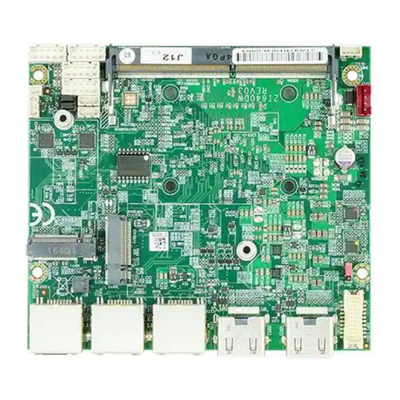
Chapter-1 General Information The 2I640DW is a 2.5" (110 x 98 mm) motherboard powered with Intel Atom® x6000E series and Celeron® J (formerly Elkhart Lake) processor & off ered the ideal platform for high performance applications. The ultra compact (110 x 98 mm) motherboard with wide range 9~24V DC power input &... -
Page 9: Major Feature
1-1 Major Feature Intel® Atom x6413E Processor 1.5GHz / 2.7GHz (Quad Core), Intel® Celeron Processor J6412 2.0GHz / 2.6GHz (Quad Core) Intel® UHD Graphics for 10th Gen Intel® Atom x6413E 500MHz / 750MHz, Intel® Celeron J6412 400MHz / 800MHz DDR4 SODIMM slot x 1, up to 32GB Support 3 x 10 / 100 / 1000 Mbps Intel LAN ports. -
Page 10: Specification
1-2 Specifi cation SOC: Intel® Atom x6413E Processor 1.5GHz / 2.7GHz (Quad Core), Intel® Celeron Processor J6412 2.0GHz / 2.6GHz (Quad Core) Memory: DDR4 SODIMM slot x 1, up to 32GB Graphics: Intel® UHD Graphics for 10th Gen Intel® Atom x6413E 500MHz / 750MHz, Intel®... -
Page 11: Installing The So-Dimm
1-3 Installing the SO-DIMM 1. Align the SO-DIMM with the connector at a 45 degree angle. 2. Press the SO-DIMM into the connector until you hear a click. - Page 12 Notices: 1. The connectors are designed to ensure the correct insertion. If you feel resistance, check t h e connectors & golden fi nger direction, and realign the card. 2. Make sure the retaining clips (on two sides of the slot) lock onto the notches of the card fi...
-
Page 13: Removing The So-Dimm
1-3-1-1 Removing the SO-DIMM 1. Release the SO-DIMM by pulling outward the two retaining clips and the SO-DIMM pops up slightly. 2. Lift the SO-DIMM out of its connector carefully. -
Page 14: Directions For Installing The M.2 B Key Mini Card
1-4 Directions for installing the M.2 B Key Mini Card 1. Unscrew the screw on the board 2. Plug in the Mini Card in a 45 angle 3. Gently push down the Mini Card and screw the screw back. -
Page 15: Chapter 2 Hardware Installation
Chapter-2 2-1 Dimension-2I640DW... -
Page 16: Layout-2I640Dw-Connector And Jumper
2-2 Layout-2I640DW-Connector and Jumper NGFF1 JAT1 NGFF2 JSB1 CBT1 CFP1 CIO1 SODIM1 HDMI1 HDMI2 CPI1 JVL1... -
Page 17: Layout-2I640Dw-Connector And Jumper Bot
2-2-1 Layout-2I640DW-Connector and Jumper Bottom SIM1... -
Page 18: Layout-2I640Dw-Function Map Top
2-3 Layout-2I640DW-Function MAP M.2 B Key 2242 PCIe x2 - based SSD USB 2.0 M.2 B Key 2242/3042 SATA-based SSD Power IN Always ON PCIe x2 - based SSD USB 2.0 USB 2.0/3.0 CMOS Data Clear Battery Wafer Front Panel... -
Page 19: Layout-2I640Dw-Function Map Bot
2-3-1 Layout-2I640DW-Function MAP USB 2.0 / 3.0 USB 2.0 / 3.0 Nano SIM... -
Page 20: Diagram-2I640Dw Top
2-4 Diagram- 2I640DW NGFF1 JAT1 NGFF2 JSB1 CBT1 CFP1 CIO1 SODIM1 HDMI1 HDMI2 CPI1 JVL1... -
Page 21: Diagram-2I640Dw Bot
2-4-1 Diagram- 2I640DW SIM1... -
Page 22: Function Map-2I640Dw Top
2-5 Function MAP- 2I110D M.2 B Key 2242 PCIe x2 - based SSD USB 2.0 M.2 B Key 2242/3042 SATA-based SSD Power IN Always ON PCIe x2 - based SSD USB 2.0/3.0 USB 2.0 CMOS Data Clear Battery Wafer Front Panel LAN1 COM1 COM2... -
Page 23: Function Map-2I640Dw Bot
2-5-1 Function MAP- 2I110D USB 2.0 / 3.0 USB 2.0 / 3.0 Nano SIM... -
Page 24: List Of Jumpers
2-6 List of Jumpers JSB1: CMOS DATA Clear JAT1: Power in always ON function JVL1: eDP panel power select 2-7 Jumper Setting Description A jumper is ON as a closed circuit with a plastic cap covering two pins. A jumper is OFF as an open circuit without the plastic cap. -
Page 25: Jsb1: Cmos Data Clear
2-8 JSB1: CMOS DATA Clear A battery must be used to retain the motherboard confi guration in CMOS RAM. Close Pin1 and pin 2 of JSB1 to store the CMOS data. To clear the CMOS, follow the procedures below: 1. Turn off the system and unplug the AC power 2. -
Page 26: Jat1: Power In Always On Function
2-9 JAT1: Power in always ON function JSB2 DESCRIPTION *1-2 Disabled Enable NOTE: Power always on function default is disabled. JSB2 Enable *Disabled 2-10 JVL1: eDP panel power select JVL1 DESCRIPTION *2-3 +3.3V Note: Attention! Check Device Power in spec JVL1 1 2 3 1 2 3... -
Page 27: Chapter 3 Connection
Chapter-3 Connection This chapter provides all necessary information of the peripheral's connections, switches and indicators. Always power off the board before you install the peripherals. 3-1 List of Connectors CBT1: CMOS Battery in 1x2 pin (1.25mm) wafer CU1: USB 3.0 type A connector CU2: USB 3.0 type A connector CU6:... -
Page 28: Cmos Battery Connector
3-2 CMOS battery connector CBT1: CMOS Battery in 1x2 pin (1.25mm) wafer PIN NO. DESCRIPTION Battery in (GND) Battery in (+3V) Note: NOTE: CBT1 for external connector can extend battery capacity. CBT1 pin1... -
Page 29: Usb Interface
3-3 USB Interface CU1 / CU2: USB 3.0 / 2.0 Type A connector PIN NO. DESCRIPTION PIN NO. DESCRIPTION USB 3.0 TX+ USB 2.0 D- USB 3.0 TX- USB 2.0 D+ USB 3.0 RX+ USB 3.0 RX- USB 3.0 RX- USB 3.0 / 2.0 USB 3.0 / 2.0 CU6 / CU7 / CU8: USB 2.0 1x4 pin (1.25mm) wafer... -
Page 30: Lan Interface
3-4 LAN Interface CL1 / CL2 / CL3: RJ45 LAN Connector PIN NO. DESCRIPTION PIN NO. DESCRIPTION TD0+/TX+ TD0-/TX- TD1+/RX+ TD2+/NC TD2-/NC TD1-/RX- TD3+/NC TD3-/NC CL1 / CL2 / CL3: RJ45 LAN Connector Speed 10 Mbps 100 Mbps 1000 Mbps Indicate Link LED Active LED... -
Page 31: Com Interface
3-5 COM interface CC1 / CC2: COM1 / COM2 2x5 pin (2.0mm) wafer (RS232 Mode) PIN NO. DESCRIPTION PIN NO. DESCRIPTION Note: 1. COM 1 / 2 Default RS232 RS485 / RS422 by BIOS control. 2. The pin9 RI can be modify to Power to supply device. The power voltage can be set +12V or +5V. -
Page 32: Front Panel Pin Header
3-6 Front Panel Pin Header CFP1: Front Panel 2x5 pin (2.0mm) wafer PIN NO. Description PIN NO. Description Power button pin Power button GND Reset pin Reset GND Power LED- Power LED+ HDD LED- HDD LED+ LAN LED- LAN LED+ CFP1 pin1... -
Page 33: Dio Interface
3-7 DIO Interface CIO1: DIO 0~3 2x5 pin (2.0mm) wafer PIN NO. Description PIN NO. Description DI-0 DO-3 DI-1 DO-2 DI-2 DO-1 DI-3 DO-0 Note: 1. DI pin default pull up 10KΩ to +5V. 2. If use need isolate circuit to control external device. 3. -
Page 34: Io Device: F75111 Cio Utility
3-7-1 IO Device: F75111 CIO Utility The Sample code source you can download from http://tprd.info/lexwiki/index.php/IO_Device:F75111_CIO_Utility Source fi le: CIO_Utility_Src_v3.0.5_w.zip Binary fi le: CIO_Utility_Bin_v3.0.5_x32_w.zip CIO_Utility_Bin_v3.0.5_x64_w.zip F75113 DLL: F75113.dll We do the demo test with a test tool which DIx connect to DOx with Relay. - Page 35 How to use this Demo Application...
- Page 36 Attention Please:You must be install vcredist_x86.exe when first time you run the F75111_DIO.exe DEMO AP, The vcredist_x86.exe include all required DLL fi le. 1. Press the select your test "2i2o", "4i4o", "4i4o*2", "F75111CIO116", "F75113CIO116", "8i+8o" 2. start test, select single mode or looptest...
- Page 37 F75111 Layout Picture Introduction F75111 Initial Internal F75111 port address (0x9c) defi ne GPIO1X, GPIO2X, GPIO3X to input or output and Enable WDT function pin Set F75111 DI/DO ( sample code as below Get Input value/Set output value ) DO: InterDigitalOutput(BYTE byteValue)) DI: InterDigitalInput() PULSE mode Sample to setting GP33, 32, 31, 30 output 1mS low pulse signal.
- Page 38 Initial internal F75111 void F75111::InitInternalF75111() this->Write_Byte(F75111_INTERNAL_ADDR,GPIO1X_CONTROL_MODE ,0x00); //set GPIO1X to Input function this->Write_Byte(F75111_INTERNAL_ADDR,GPIO3X_CONTROL_MODE ,0x00); //set GPIO3X to Input function this->Write_Byte(F75111_INTERNAL_ADDR,GPIO2X_CONTROL_MODE ,0xFF); //set GPIO2X to Output function this->Write_Byte(F75111_INTERNAL_ADDR,F75111_CONFIGURATION, 0x03); //Enable WDT OUT function Set output value void F75111::InterDigitalOutput(BYTE byteValue) BYTE byteData = 0; byteData = (byteData &...
- Page 39 Get Input value BYTE F75111::InterDigitalInput() BYTE byteGPIO1X = 0; BYTE byteGPIO3X = 0; BYTE byteData = 0; this->Read_Byte(F75111_INTERNAL_ADDR,GPIO1X_INPUT_DATA,&byteGPIO1X) ; // Get value from GPIO1X this->Read_Byte(F75111_INTERNAL_ADDR,GPIO3X_INPUT_DATA,&byteGPIO3X) ; // Get value from GPIO3X byteGPIO1X = byteGPIO1X & 0xF0; // Mask unuseful value byteGPIO3X = byteGPIO3X &...
- Page 40 defi ne F75111 pin in F75111.h //----------------------------------------------------------------------------------------------------------------------------------------------------- #defi ne F75111_INTERNAL_ADDR 0x9C // OnBoard F75111 Chipset #defi ne F75111_EXTERNAL_ADDR 0x6E // External F75111 Chipset //----------------------------------------------------------------------------------------------------------------------------------------------------- #defi ne F75111_CONFIGURATION 0x03 // Confi gure GPIO13 to WDT2 Function //----------------------------------------------------------------------------------------------------------------------------------------------------- #defi ne GPIO1X_CONTROL_MODE 0x10 // Select Output Mode or Input Mode #defi...
-
Page 41: Io Device:f75111 Cio Utility Cio116
3-7-2 IO Device:F75111 CIO Utility CIO116 The Sample code source you can download from Source fi le: CIO_Utility_Src_v3.0.3.tar.gz Binary fi le: CIO_Utility_Bin_v3.0.3_x32.tar.gz CIO_Utility_Bin_v3.0.3_x64.tar.gz http://tprd.info/lexwiki/index.php/IO_Device:F75111_CIO_Utility_CIO116 How to use this Demo Application Before executing the program began, Please switch to the highest authority, continued second F75111, chmod 777 and root: \ 1. - Page 42 F75111 Layout Picture Introduction Initial Internal F75111 port address (0x9c) defi ne GPIO1X, GPIO2X, GPIO3X to input or output and Enable WDT function pin Set F75111 DI/DO ( sample code as below Get Input value/Set output value ) DO: InterDigitalOutput(BYTE byteValue)) DI: InterDigitalInput() PULSE mode Sample to setting GP33, 32, 31, 30 output 1mS low pulse signal.
- Page 43 Initial internal F75111 void F75111::InitInternalF75111() this->Write_Byte(F75111_INTERNAL_ADDR,GPIO1X_CONTROL_MODE ,0x00); //set GPIO1X to Input function this->Write_Byte(F75111_INTERNAL_ADDR,GPIO3X_CONTROL_MODE ,0x00); //set GPIO3X to Input function this->Write_Byte(F75111_INTERNAL_ADDR,GPIO2X_CONTROL_MODE ,0xFF); //set GPIO2X to Output function this->Write_Byte(F75111_INTERNAL_ADDR,F75111_CONFIGURATION ,0x03); //Enable WDT OUT function Set output value void F75111::InterDigitalOutput(BYTE byteValue) BYTE byteData = 0; byteData = (byteData &...
- Page 44 Get Input value BYTE F75111::InterDigitalInput() BYTE byteGPIO1X = 0; BYTE byteGPIO3X = 0; BYTE byteData = 0; this->Read_Byte(F75111_INTERNAL_ADDR,GPIO1X_INPUT_DATA,&byteGPIO1X) ; // Get value from GPIO1X this->Read_Byte(F75111_INTERNAL_ADDR,GPIO3X_INPUT_DATA,&byteGPIO3X) ; // Get value from GPIO3X byteGPIO1X = byteGPIO1X & 0xF0; // Mask unuseful value byteGPIO3X = byteGPIO3X &...
- Page 45 defi ne F75111 pin in F75111.h //-------------------------------------------------------------------------------------------------------- #defi ne F75111_INTERNAL_ADDR 0x9C // OnBoard F75111 Chipset #defi ne F75111_EXTERNAL_ADDR 0x6E // External F75111 Chipset //-------------------------------------------------------------------------------------------------------- #defi ne F75111_CONFIGURATION 0x03 // Confi gure GPIO13 to WDT2 Function //-------------------------------------------------------------------------------------------------------- #defi ne GPIO1X_CONTROL_MODE 0x10 // Select Output Mode or Input Mode #defi...
-
Page 46: Co1: I2C 1X4 Pin (1.25Mm) Wafer
3-8 CO1: SMBus 1x4 pin (1.25mm) wafer PIN NO. DESCRIPTION PIN NO. DESCRIPTION +3.3V SMB-Clock SMB-Data pin1 3-9 CPI1: DC Power input 1x4 pin (2.0mm) wafer (RED) PIN NO. DESCRIPTION DC-IN Note: Very important check DC-in Voltage. pin1... -
Page 47: Display Interface
3-10 Display Interface HDMI1 / HDMI2: HDMI type A connector PIN NO. DESCRIPTION PIN NO. DESCRIPTION TMDS DATA2+ TMDS DATA2- TMDS DATA1+ TMDS DATA1- TMDS DATA0+ TMDS DATA0- TMDS CLK+ TMDS CLK- DDC CLOCK DDC DATA H.P. Detect HDMI1 HDMI2 HDMI HDMI... - Page 48 DP1 / DP2: Display Port connector (option) PIN NO. DESCRIPTION PIN NO. DESCRIPTION Lane0+ Lane0- Lane1+ Lane1- Lane2+ Lane2- Lane3+ Lane3- AUX_CH+ AUX_CH- H.P. Detect +3.3V...
- Page 49 EDP1: eDP interface 2x10 pin (1.25mm) wafer PIN NO. DESCRIPTION PIN NO. DESCRIPTION Lane-0-DATA- +12V Lane-0-DATA+ +12V Lane-1-DATA- Lane-1-DATA+ Backlight Enable PWM dimming I2C Clock +LCD (5V or 3.3V) I2C Data +LCD (5V or 3.3V) eDP Aux+ +LCD (5V or 3.3V) eDP Aux- EDP_HPD Note:...
-
Page 50: Sim1: Nano Sim Card Push-Push
3-11 SIM1: Nano SIM Card Push-Push Follow ISO 7816-2 Smart Card Standard. PIN NO. DESCRIPTION PIN NO. DESCRIPTION DATA SIM1 Nano SIM... -
Page 51: Ngff1: Pci Express M.2 B Key 2242 H=8.5 Sockets 75Pin
3-12 NGFF1: PCI Express M.2 B key 2242 H=8.5 sockets 75pin PIN NO. DESCRIPTION PIN NO. DESCRIPTION +3.3V +3.3V FULL_CARD_PWR USB2.0_P USB2.0_N M2_LED B Key notch M2_PERn1 M2_PERp1 M2_PETn1 M2_PETp1 M2_PERn0 / SATA-RX+ M2_PERp0 / SATA-RX- M2_PETn0 / SATA-TX- M2_PETp0 / SATA-TX+ PREST SRCCLKREQ_N PCIE_CLK_N0... - Page 52 PIN NO. DESCRIPTION PIN NO. DESCRIPTION CFG1_SATA_PCIE +3.3V +3.3V +3.3V Note: 1. NGFF1 support PCIe x2 / SATA-SSD Auto detect. 2. NGFF1 VCC voltage support +3.3V. NGFF1...
-
Page 53: Ngff2: Pci Express M.2 B Key 2242 / 3042 H=8.5 Sockets 75Pin
3-13 NGFF2: PCI Express M.2 B key 2242 / 3042 H=8.5 sockets 75pin PIN NO. DESCRIPTION PIN NO. DESCRIPTION CFG3_USB3_PCIE +3.3V / +3.7V +3.3V / +3.7V FULL_CARD_PWR USB2.0_P W_DISABLE_1 USB2.0_N M2_LED B Key notch W_DISABLE_2 M2_PERn1_U3Rn SIM_RST_M2 M2_PERp1_U3Rp SIM_CLK_M2 SIM_DATA_M2 M2_PETn1_U3Tn SIM_PWR_M2 M2_PETp1_U3Tp... -
Page 54: Crfp1: Antenna Control 1X4 Pin (1.25Mm) Wafer (Oem)
PIN NO. DESCRIPTION PIN NO. DESCRIPTION ANTCTL1 ANTCTL2 SIM_DET MD_RESET_N +3.3V / +3.7V +3.3V / +3.7V +3.3V / +3.7V CONFIG_2 Note: 1. NGFF2 support USB 3.0 / PCIe x2 Auto detect. 2. VCC voltage default support +3.3V. 3. BOM control, if need 4G LTE device VCC voltage is +3.7V. NGFF2 3-14 CRFP1: Antenna control 1x4 pin (1.25mm) wafer (OEM) PIN NO. -
Page 55: Introduction Of Bios
Chapter-4 Introduction of BIOS The BIOS is a program located in the Flash Memory on the motherboard. This program is a bridge between motherboard and operating system. When you start the computer, the BIOS program gains control. The BIOS first operates an auto-diagnostic test called POST (Power on Self Test) for all the necessary hardware, it detects the entire hardware devices and configures the parameters of the hardware synchronization. -
Page 56: Bios Menu Screen & Function Keys
4-2 BIOS Menu Screen & Function Keys In the above BIOS Setup main menu of, you can see several options. We will explain these options step by step in the following pages of this chapter, but let us fi rst see a short description of the function keys you may use here: ●... -
Page 57: Getting Help
4-3 Getting Help Status Page Setup Menu / Option Page Setup Menu Press F1 to pop up a help window that describes the appropriate keys to use and the possible selections for the highlighted item. To exit the Help Window, press <Esc>. 4-4 Menu Bars There are six menu bars on top of BIOS screen: Main To change system basic confi... -
Page 58: Main
4-5 Main Main menu screen includes some basic system information. Highlight the item and then use the <+> or <-> and numerical keyboard keys to select the value you want in each item. System Date Set the Date. Please use [Tab] to switch between data elements. System Time Set the Time. -
Page 59: Advanced
4-6 Advanced Boot Confi guration Please refer section 4-6-1 SOC Confi g Confi guration Please refer section 4-6-2 SIO F81804 Please refer section 4-6-3 NVM Express information Please refer section 4-6-4... -
Page 60: Boot Configuration
4-6-1 Boot Confi guration To select Power-on state for NumLock, default is <off >... -
Page 61: Soc Config Configuration
4-6-2 SOC Confi g Confi guration ACPI Settings Please refer section 4-6-2-1 System Agent (SA) Confi guration Please refer section 4-6-2-2 PCH-IO Confi guration Please refer section 4-6-2-3 PCH-FW Confi guration Please refer section 4-6-2-4... -
Page 62: Acpi Settings
4-6-2-1 ► ACPI Settings ACPI S3 Support To enable BIOS support security device or not, default is Enabled. -
Page 63: System Agent (Sa) Configuration
4-6-2-2 ► System Agent (SA) Confi guration... - Page 64 Graphic Confi guration First Boot Display To select First Boot Display priority, there are eDP, DDI1 HDMI, DDI2 HDMI, default is eDP. Second Boot Display To select Second Boot Display priority, there are DDI1 HDMI, DDI2 HDMI, default is DDI1 HDMI.
-
Page 65: Pch-Io Configuration
4-6-2-3 ► PCH-IO Confi guration PCI Express Confi guration Please refer section 4-6-2-3-1 SATA Confi guration Please refer section 4-6-2-3-2... -
Page 66: Pci Express Configuration
4-6-2-3-1 ► PCI Express Confi guration... - Page 67 To select NGFF1 device enabled or not and to change the PCIe Speed, there are Auto, Gen1, Gen2, Gen3, default is Auto...
-
Page 68: Sata Configuration
4-6-2-3-2 ► SATA Confi guration To select NGFF1 M.2 SATA device enabled or not. -
Page 69: Pch-Fw Configuration
4-6-2-4 ► PCH-FW Confi guration... -
Page 70: Sio F81804
4-6-3 SIO F81804 UART Port 1 Confi guration Please refer section 4-6-3-1 UART Port 2 Confi guration Please refer section 4-6-3-2 Hardware Monitor Please refer section 4-6-3-3 Restore on Power Loss Please refer section 4-6-3-4... -
Page 71: Uart Port 1 Configuration
4-6-3-1 ► UART Port 1 Confi guration To Enable Serial port or not, default is Enabled. - Page 72 Base I/O Address, default is 3F8h.
- Page 73 Interrupt, default is IRQ4.
- Page 74 Peripheral, to select the Serial port to RS232 / RS422 / RS485, default is RS232.
-
Page 75: Uart Port 2 Configuration
4-6-3-2 ► UART Port 2 Confi guration To Enable Serial port or not, default is Enabled. - Page 76 Base I/O Address, default is 2F8h.
- Page 77 Interrupt, default is IRQ3.
- Page 78 Peripheral, to select the Serial port to RS232 / RS422 / RS485, default is RS232.
-
Page 79: Harware Monitor
4-6-3-3 ► Hardware Monitor Press [Enter] to view PC health status. This section shows the status of your CPU, Fan, and overall system. This is only available when there is Hardware Monitor function onboard. -
Page 80: Restore On Power Loss
4-6-3-4 Restore On Power Loss To select the power behavior after power fail, default is last state. -
Page 81: Nvm Express Information
4-6-4 NVM Express Information Press [Enter] to view the NVMe storage devices information. -
Page 82: Security
4-7 Security TrEE Protocol Version There are 1.0 and 1.1 versions. TPM Availability To select TPM available or hidden TPM Operation... - Page 83 To select TPM operations...
- Page 84 Set Supervisor Password To set up an Supervisor password...
-
Page 85: Power
4-8 Power Wake On LAN1 To select S3, S5 or S3 / S5 wake on LAN1, default is Disabled. Wake On USB To select S3 wake on USB, default is Disabled. Wake On RTC The optional settings are: Disabled (default), By every day, By day of month. -
Page 86: Boot
4-9 Boot Quiet Boot The optional settings are: Enabled (default), Disabled. Network Stack The optional settings are: Enabled, Disabled (default). -
Page 87: Save & Exit
4-10 Save & Exit Exit Saving Changes Save confi guration and reset Exit Discarding Changes Reset without saving the changes Load Optimal Defaults To restore the optimal default for all the setup options... -
Page 88: How To Update Insyde Bios
STEP 3. Copy the latest BIOS for your LEX motherboard from our website to your bootable disc. STEP 4. (Here take 2I640DW as an example, please enter your motherboard’s name) Insert your bootable disc into X: (X could be C:, A: or others. -
Page 89: Appendix B: Resolution List
Appendix B: Resolution list 640 x 480 x ( 256 / 16bit / 32bit ) 800 x 600 x ( 256 / 16bit / 32bit ) 1024 x 768 x ( 256 / 16bit / 32bit ) 1152 x 864 x ( 256 / 16bit / 32bit ) 1280 x 600 x ( 256 / 16bit / 32bit ) 1280 x 720 x ( 256 / 16bit / 32bit ) 1280 x 768 x ( 256 / 16bit / 32bit )
Need help?
Do you have a question about the 2I640DW and is the answer not in the manual?
Questions and answers