Table of Contents
Advertisement
Quick Links
Advertisement
Table of Contents

Related Manuals for Lattice Semiconductor LatticeMico32/DSP


Summary of Contents for Lattice Semiconductor LatticeMico32/DSP
- Page 1 LatticeMico32/DSP Development Board User’s Guide October 2007 Revision: EB17_01.4...
- Page 2 User’s Guide Introduction This document describes the features and functionality of the LatticeMico32/DSP Development Board. This board is designed as a hardware platform for design and development with the LatticeMico32 microprocessor, as well as for the LatticeMico8 microcontroller, and for various DSP functions.
-
Page 3: Getting Started
• LatticeMico32 Development Kit User’s Guide : This guide includes a tutorial for using the LatticeMico32 Sys- tem software with the LatticeMico32/DSP Development Board. • LatticeMico32/DSP Demonstration : This includes a documented demonstration of a DSP example using the LatticeMico32/DSP Development board. -
Page 4: Peripheral Interfaces
SODIMM DDR 400 Setting (X18) Jumper Set to below DDR400 memory use. 1 and 2 Peripheral Interfaces This section describes all peripheral interfaces of the LatticeMico32/DSP Development Board in alphabetical order. Figure 2 shows the position of peripheral interfaces available on the board. -
Page 5: Audio Interface
LatticeMico32/DSP Development Board Lattice Semiconductor User’s Guide Figure 2. Peripheral Interfaces Microphone Ethernet Input 10/100M Audio RS232 Mini USB Power Plug Line In OTG-Connector Line Out USB Host Connector 2.5V Testpoint 3.3V Testpoint DDR SDRAM Socket X4 Testpoint 1.2V Testpoint... - Page 6 LatticeMico32/DSP Development Board Lattice Semiconductor User’s Guide Table 2. Audio Codec U1001 Pin Definitions Signal Name FPGA Pin Signal Name FPGA Pin CODEC BCLK CODEC CS# CODEC DIN CODEC DOUT CODEC LRCIN CODEC LRCOUT CODEC MCLK CODEC SCLK CODEC SDIN CODEC MODE The signal CODEC CS# has a pull-up resistor of 10 k Ω...
- Page 7 LatticeMico32/DSP Development Board Lattice Semiconductor User’s Guide Table 3. DDR SODIMM Socket (X4) - Data Bus, n.c..Not Connected (Continued) DDR DQ8 DDR DQ24 DDR DQ9 DDR DQ25 DDR DQ10 DDR DQ26 DDR DQ11 DDR DQ27 DDR DQ12 DDR DQ28...
- Page 8 LatticeMico32/DSP Development Board Lattice Semiconductor User’s Guide Expansion Connector The expansion connector provides 46 user I/Os connected to the FPGA. The remaining pins serve as power and clock supplies for expansion boards. The expansion connector is configured as two 2x20 100mil centered pin head- ers (X12 and X13).
- Page 9 LatticeMico32/DSP Development Board Lattice Semiconductor User’s Guide Table 8. Expansion Connector X13 (Continued) EXPCON IO24 — EXPCON IO25 EXPCON IO26 EXPCON IO27 CARDSEL# EXPCON IO28 — ispDOWNLOAD Cable Connector There are two ways to configure the programmable Lattice devices on the board. The USB connector requires a standard USB cable, and is described later in this document.
- Page 10 LatticeMico32/DSP Development Board Lattice Semiconductor User’s Guide Table 10. High-Speed Connector X14 Pin Definition Signal Name FPGA Pin Signal Name FPGA Pin HSCON DAT0- HSCON DAT0+ — — HSCON DAT1- HSCON DAT1+ — — HSCON DAT2- HSCON DAT2+ — —...
- Page 11 LatticeMico32/DSP Development Board Lattice Semiconductor User’s Guide Table 12. Serial Interface X1C Pin Definitions Signal Direction Sub-D Pin RS232 Function FPGA Pin RS TXD LVTTL Transmit Data RS RTS LVTTL Request to Send RS RXD LVTTL Receive Data RS CTS LVTTL...
- Page 12 LatticeMico32/DSP Development Board Lattice Semiconductor User’s Guide Table 14. Additional USB GPIO Connections (U0702, U0704, and U0704) Signal Name FPGA Pin Signal Name FPGA Pin U0703:1 USB PWEN0 U0703:2 USB OC0# U0703:4 USB PWEN1 U0703:3 USB OC1# U0704:1 USB PWEN2...
-
Page 13: Vga Interface
LatticeMico32/DSP Development Board Lattice Semiconductor User’s Guide Table 15. Connections Between the USB Controller (CY7C68013A) and the MachXO Device (Continued) GP CTL2 GP CTL3 GP CTL4 GP CTL5 GP T0 GP T1 GP T2 GP BKPT USB CLK O GP IFCLK... -
Page 14: User Interface
LatticeMico32/DSP Development Board Lattice Semiconductor User’s Guide User Interface Figure 6 shows the position of the user interface elements. Figure 6. User Interface Features 2.5 V LED (green) 3.3 V LED (green) 4 x DIP Switches FPGA Configuration LED (blue) - Page 15 LatticeMico32/DSP Development Board Lattice Semiconductor User’s Guide 7-Segment Display The 7-segment display is wired as follows: Table 17. 7 Segment Display U0502 Pin Definition Signal Name FPGA Pin Signal Name FPGA Pin SED_A# SED_E# SED_B# SED_F# SED_C# SED_G# SED_D# D, P...
-
Page 16: Key Matrix
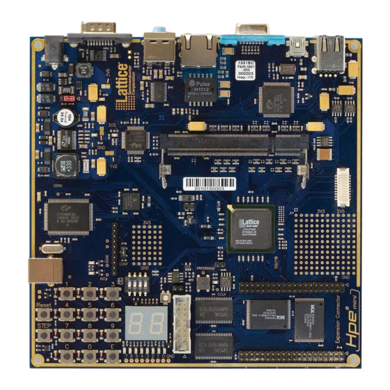
LatticeMico32/DSP Development Board Lattice Semiconductor User’s Guide Key Matrix The board also features a key matrix with 12 push-buttons, which are not debounced. They must be driven with three column lines and can be read with four rows. The following table shows the connections. - Page 17 LatticeMico32/DSP Development Board Lattice Semiconductor User’s Guide Components Figure 8 illustrates the position of major components. Figure 8. Components Audio Codec Controller Ethernet MachXO USB Controller FPGA for the LFEC33 Configuration 12 x 12 Prototyping Area of the FPGA 8 x 6 Prototyping...
- Page 18 LatticeMico32/DSP Development Board Lattice Semiconductor User’s Guide 12 x 12 FPGA Prototyping Area of The FPGA A 12x12 prototyping area is available on the right side of the board. The lead-wire spacing of the prototyping area is 100mil (2.54 mm). Figure 10 shows the prototyping area in top view. 14 plated-through-holes on its left side are connected to the FPGA.
- Page 19 LatticeMico32/DSP Development Board Lattice Semiconductor User’s Guide Figure 9. Schematic Illustration of the Prototyping Area VCC3V3 VCC2V5 BB2V5_IO[9:0] BB3V3_IO[11:0] TP0901 TP0913 TP0925 TP0937 TP0949 TP0961 TP0973 TP0985 TP0997 TP09109 TP09121 TP09133 BB3V3_IO0 BB2V5_IO0 TP0902 TP0914 TP0926 TP0938 TP0950 TP0962 TP0974...
- Page 20 LatticeMico32/DSP Development Board Lattice Semiconductor User’s Guide Table 23. MachXO Connections for the 8x6 Prototyping Area (Continued) — TP0343 — TP0344 — TP0345 — TP0346 — TP0347 — TP0348 Figure 10. Schematic Illustration of the Prototyping Area VCC3V3 TP0301 TP0302...
-
Page 21: Spi Flash
Sample programs for the FPGA are available on-line as well. These can be found at www.latticesemi.com/boards. Select FPGA/FPSC Boards -> LatticeMico32/DSP Development board and click on the Design Files link. For further information please consult the LatticeECP/EC Family Data Sheet. -
Page 22: Power Supply
LatticeMico32/DSP Development Board Lattice Semiconductor User’s Guide 2. Click Select to open the Select Device dialog box. 3. From the Device Family drop-down list, select FPGA Loader. The FPGA Loader opens and displays a setup menu in the left pane and instructions in the right pane. -
Page 23: Electrical Specifications
LatticeMico32/DSP Development Board Lattice Semiconductor User’s Guide 1. Check the 3.3V and 2.5V LEDs to ensure that the power supply is working correctly. 2. Make sure that the INIT LED is lit. 3. Load test program 1 4. Make sure the FPGA has been configured properly (DONE LED must be lit). - Page 24 LatticeMico32/DSP Development Board Lattice Semiconductor User’s Guide Table 25. Pin Table (Continued) Pin Name Signal Name Appliance BB3V3 IO7 FPGA Prototyping Area BB3V3 IO8 FPGA Prototyping Area BB3V3 IO9 FPGA Prototyping Area CARDSEL# FPGA Prototyping Area CCLK Configuration CCLK Configuration CFG0 Configuration...
- Page 25 LatticeMico32/DSP Development Board Lattice Semiconductor User’s Guide Table 25. Pin Table (Continued) Pin Name Signal Name Appliance DDR CKE1 DDR RAM DDR DM0 DDR RAM DDR DM1 DDR RAM DDR DM2 DDR RAM DDR DM3 DDR RAM DDR DQ0 DDR RAM...
- Page 26 LatticeMico32/DSP Development Board Lattice Semiconductor User’s Guide Table 25. Pin Table (Continued) Pin Name Signal Name Appliance DDR VREF DDR RAM DDR VREF DDR RAM DDR WE# DDR RAM DOUT Configuration DSW0 DIP Switch DSW1 DIP Switch DSW2 DIP Switch...
- Page 27 LatticeMico32/DSP Development Board Lattice Semiconductor User’s Guide Table 25. Pin Table (Continued) Pin Name Signal Name Appliance EXPCON IO19 Expansion Connector EXPCON IO2 Expansion Connector EXPCON IO20 Expansion Connector EXPCON IO21 Expansion Connector EXPCON IO22 Expansion Connector EXPCON IO23 Expansion Connector...
- Page 28 LatticeMico32/DSP Development Board Lattice Semiconductor User’s Guide Table 25. Pin Table (Continued) Pin Name Signal Name Appliance HS DAT1+ High-speed LVDS Connector HS DAT3- High-speed LVDS Connector HS DAT3+ High-speed LVDS Connector HS DAT0- High-speed LVDS Connector HS DAT0+ High-speed LVDS Connector...
- Page 29 LatticeMico32/DSP Development Board Lattice Semiconductor User’s Guide Table 25. Pin Table (Continued) Pin Name Signal Name Appliance AA15 MEMORY A22 FLASH/SRAM AA19 MEMORY A3 FLASH/SRAM MEMORY A4 FLASH/SRAM AB18 MEMORY A5 FLASH/SRAM AA18 MEMORY A6 FLASH/SRAM MEMORY A7 FLASH/SRAM MEMORY A8...
- Page 30 LatticeMico32/DSP Development Board Lattice Semiconductor User’s Guide Table 25. Pin Table (Continued) Pin Name Signal Name Appliance RS RTS LVTTL RS233 RS RXD LVTTL RS234 RS TXD LVTTL RS235 SEG A# LCD, 7-Segment Display SEG B# LCD, 7-Segment Display SEG C#...
- Page 31 LatticeMico32/DSP Development Board Lattice Semiconductor User’s Guide Table 25. Pin Table (Continued) Pin Name Signal Name Appliance USB GPIO22 USB GPIO23 USB GPIO24 USB GPIO25 USB GPIO26 USB GPIO27 USB GPIO28 USB GPIO3 USB GPIO4 USB GPIO5 USB GPIO6 USB GPIO7...
- Page 32 LatticeMico32/DSP Development Board Lattice Semiconductor User’s Guide Figure 11. LatticeECP33 BGA Pinout PCLK TDQS46 PCLK VGA_ VGA_ VGA_ VGA_ VGA_ USB_ USB_ T0_0 DDR DQ0 DDR DQ2 DDR DQ4 DDR DQ6 C0_0 VSYNC HSYNC GPIO5 GPIO11 CK0- CKE0 CAS# CK1+...
-
Page 33: Ordering Information
Updated FPGA Pin column in the Serial Interface X1C Pin Definitions table. © 2007 Lattice Semiconductor Corp. All Lattice trademarks, registered trademarks, patents, and disclaimers are as listed at www.latticesemi.com/legal. All other brand or product names are trademarks or registered trademarks of their respective holders. -
Page 34: Appendix A. Schematics
LatticeMico32/DSP Development Board Lattice Semiconductor User’s Guide Appendix A. Schematics Figure 12. - Page 35 LatticeMico32/DSP Development Board Lattice Semiconductor User’s Guide Figure 13.
- Page 36 LatticeMico32/DSP Development Board Lattice Semiconductor User’s Guide Figure 14.
- Page 37 LatticeMico32/DSP Development Board Lattice Semiconductor User’s Guide Figure 15.
- Page 38 LatticeMico32/DSP Development Board Lattice Semiconductor User’s Guide Figure 16.
- Page 39 LatticeMico32/DSP Development Board Lattice Semiconductor User’s Guide Figure 17.
- Page 40 LatticeMico32/DSP Development Board Lattice Semiconductor User’s Guide Figure 18.
- Page 41 LatticeMico32/DSP Development Board Lattice Semiconductor User’s Guide Figure 19.
- Page 42 LatticeMico32/DSP Development Board Lattice Semiconductor User’s Guide Figure 20.
- Page 43 LatticeMico32/DSP Development Board Lattice Semiconductor User’s Guide Figure 21.
-
Page 44: Appendix B. Assembly Diagram
LatticeMico32/DSP Development Board Lattice Semiconductor User’s Guide Appendix B. Assembly Diagram Note: Figures 23-26 provide an enlargement of each numbered section in Figure 22. Figure 22. Assembly Diagram... - Page 45 LatticeMico32/DSP Development Board Lattice Semiconductor User’s Guide Figure 23. Assembly Diagram, Section 1 Detail...
- Page 46 LatticeMico32/DSP Development Board Lattice Semiconductor User’s Guide Figure 24. Assembly Diagram, Section 2 Detail...
- Page 47 LatticeMico32/DSP Development Board Lattice Semiconductor User’s Guide Figure 25. Assembly Diagram, Section 3 Detail...
- Page 48 LatticeMico32/DSP Development Board Lattice Semiconductor User’s Guide Figure 26. Assembly Diagram, Section 4 Detail...
- Page 49 Mouser Electronics Authorized Distributor Click to View Pricing, Inventory, Delivery & Lifecycle Information: Lattice LS-ECP33-BASE-PC-N...