Lattice Semiconductor CrossLink-NX User Manual
Hide thumbs
Also See for CrossLink-NX:
- User manual (54 pages) ,
- Quick start manual (15 pages) ,
- Quick start (2 pages)

Related Manuals for Lattice Semiconductor CrossLink-NX


Summary of Contents for Lattice Semiconductor CrossLink-NX
- Page 1 CrossLink-NX Evaluation Board User Guide FPGA-EB-02028-1.3 November 2020 Arrow.com. Downloaded from...
- Page 2 The information provided in this document is proprietary to Lattice Semiconductor, and Lattice reserves the right to make any changes to the information in this document or to any products at any time without notice.
-
Page 3: Table Of Contents
Revision History .................................. 57 © 2019-2020 Lattice Semiconductor Corp. All Lattice trademarks, registered trademarks, patents, and disclaimers are as listed at www.latticesemi.com/legal. All other brand or product names are trademarks or registered trademarks of their respective holders. The specifications and information herein are subject to change without notice. - Page 4 Table 11.1. Ordering Information ............................30 © 2019-2020 Lattice Semiconductor Corp. All Lattice trademarks, registered trademarks, patents, and disclaimers are as listed at www.latticesemi.com/legal. All other brand or product names are trademarks or registered trademarks of their respective holders. The specifications and information herein are subject to change without notice.
-
Page 5: Acronyms In This Document
Universal Serial Bus © 2019-2020 Lattice Semiconductor Corp. All Lattice trademarks, registered trademarks, patents, and disclaimers are as listed at www.latticesemi.com/legal. All other brand or product names are trademarks or registered trademarks of their respective holders. The specifications and information herein are subject to change without notice. -
Page 6: Introduction
The CrossLink-NX Evaluation Board features the CrossLink-NX FPGA in the 400-ball caBGA package (LIFCL-40-9BG400C) w the ability to expand the usability of the CrossLink-NX with Raspberry Pi, PMOD, FMC LPC connector, along with access to PCIe channel. 118 wide range I/O and 37 high speed differential pairs are available for user-defined applications. -
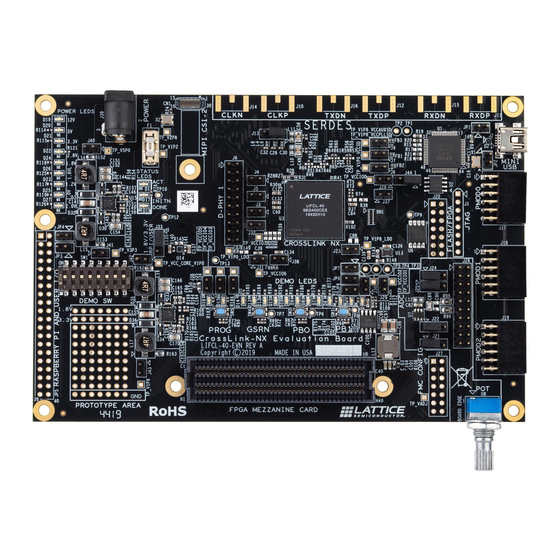
Page 7: Figure 1.1. Top View Of Crosslink-Nx Evaluation Board
Figure 1.1. Top View of CrossLink-NX Evaluation Board © 2019-2020 Lattice Semiconductor Corp. All Lattice trademarks, registered trademarks, patents, and disclaimers are as listed at www.latticesemi.com/legal. All other brand or product names are trademarks or registered trademarks of their respective holders. The specifications and information herein are subject to change without n FPGA-EB-02028-1.3... -
Page 8: Figure 1.2. Bottom View Of Crosslink-Nx Evaluation Board
Figure 1.2. Bottom View of CrossLink-NX Evaluation Board © 2019-2020 Lattice Semiconductor Corp. All Lattice trademarks, registered trademarks, patents, and disclaimers are as listed at www.latticesemi.com/legal. All other brand or product names are trademarks or registered trademarks of their respective holders. The specifications and information herein are subject to change without n Arrow.com. -
Page 9: Figure 1.3. Silkscreen Of Crosslink-Nx Evaluation Board
Figure 1.3. Silkscreen of CrossLink-NX Evaluation Board © 2019-2020 Lattice Semiconductor Corp. All Lattice trademarks, registered trademarks, patents, and disclaimers are as listed at www.latticesemi.com/legal. All other brand or product names are trademarks or registered trademarks of their respective holders. The specifications and information herein are subject to change without n FPGA-EB-02028-1.3... -
Page 10: Figure 1.4. Silkscreen Of Crosslink-Nx Evaluation Board (Bottom)
Figure 1.4. Silkscreen of CrossLink-NX Evaluation Board (Bottom) © 2019-2020 Lattice Semiconductor Corp. All Lattice trademarks, registered trademarks, patents, and disclaimers are as listed at www.latticesemi.com/legal. All other brand or product names are trademarks or registered trademarks of their respective holders. The specifications and information herein are subject to change without n Arrow.com. -
Page 11: Crosslink-Nx Device
1.4. Applying Power to the Board Power LEDs light after applying 12 V power to CrossLink-NX Evaluation Board to indicate the board is functioning. An Early I/O demo design is programmed into on-board boot flash as the default pattern. With this pattern, LED0 (D3) (mapped an early I/O) immediately turns on as soon as 12 V power is supplied to the board. -
Page 12: Jumpers And Test Connection
Figure 2.1. Top View of CrossLink-NX Evaluation Board – Jumper Locations © 2019-2020 Lattice Semiconductor Corp. All Lattice trademarks, registered trademarks, patents, and disclaimers are as listed at www.latticesemi.com/legal. All other brand or product names are trademarks or registered trademarks of their respective holders. The specifications and information herein are subject to change without n Arrow.com. -
Page 13: Table 2.1. Jumper Table
*Note: Only one jumper at a time. Otherwise, damage could occur. © 2019-2020 Lattice Semiconductor Corp. All Lattice trademarks, registered trademarks, patents, and disclaimers are as listed at www.latticesemi.com/legal. All other brand or product names are trademarks or registered trademarks of their respective holders. The specifications and information herein are subject to change without notice. -
Page 14: Power Scheme
CrossLink-NX Evaluation Board User Guide 3. Power Scheme The CrossLink-NX Evaluation Board has most of its power supplied by onboard regulators powered by an external 12 V power. Refer to Appendix A. CrossLink-NX Evaluation Board Schematics to see the details of these power supply options. -
Page 15: Programming And I 2 C
USB cable from a PC with Radiant Programmer tool installed to the mini USB connector on the board (J2). A mini USB to USB-A cable is included in the CrossLink-NX Evaluation Kit. The USB hub on the PC detects the cable of the USB function on Port 0, making the built-in cable available for use with the Radiant programming software. -
Page 16: Jtag To Mspi Pass-Through Interface
(FPGA-TN-02099). © 2019-2020 Lattice Semiconductor Corp. All Lattice trademarks, registered trademarks, patents, and disclaimers are as listed at www.latticesemi.com/legal. All other brand or product names are trademarks or registered trademarks of their respective holders. The specifications and information herein are subject to change without notice. -
Page 17: Other Jtag Configuration Pins
(FPGA-TN-02099). © 2019-2020 Lattice Semiconductor Corp. All Lattice trademarks, registered trademarks, patents, and disclaimers are as listed at www.latticesemi.com/legal. All other brand or product names are trademarks or registered trademarks of their respective holders. The specifications and information herein are subject to change without notice. -
Page 18: Crosslink-Nx Clock Sources
Insert R54 & R56, remove R65 & R66 © 2019-2020 Lattice Semiconductor Corp. All Lattice trademarks, registered trademarks, patents, and disclaimers are as listed at www.latticesemi.com/legal. All other brand or product names are trademarks or registered trademarks of their respective holders. The specifications and information herein are subject to change without notice. -
Page 19: Control Buses - I C, Uart, And Spi
The board provides support for UART configuration by providing an uninstalled connection between the FTDI and CrossLink-NX. Two 0 Ω resistors (R16 and R17) can be installed to connect Port 1 to two general purpose I/O (PR8A/F16 and PR10A/F18) in Bank 6 as shown in Figure 6.1. -
Page 20: Spi Topology
6.3.1. SPI Configuration One of the major functions of SPI connections on the board is to support CrossLink-NX configuration from the SPI Flash or the Parallel Configuration Header. The CrossLink-NX Evaluation Board can support both Master SPI (MSPI) and Slave SPI (SSPI) modes for CrossLink-NX configuration. -
Page 21: Leds And Switches
7.1. DIP Switch Eight CrossLink-NX pins are connected to the SW1 DIP switch to allow for manually actuated inputs to the FPGA. One side of each switch is connected to GPIOs within the VCCIO2 bank and pulled up through 4.7 kΩ resistors. The other side is grounded. -
Page 22: General Purpose Leds
CrossLink-NX Evaluation Board User Guide 7.3. General Purpose LEDs The CrossLink-NX Evaluation Board provides fourteen LEDs that are connected to I/O within Bank 1 & 0. The LEDs are lighted when the output is driven LOW. Table 7.3. General Purpose LED Signals... -
Page 23: Headers/Connectors And Lifcl-40 Device Ball Mapping
T6 Y18 © 2019-2020 Lattice Semiconductor Corp. All Lattice trademarks, registered trademarks, patents, and disclaimers are as listed at www.latticesemi.com/legal. All other brand or product names are trademarks or registered trademarks of their respective holders. The specifications and information herein are subject to change without notice. - Page 24 — © 2019-2020 Lattice Semiconductor Corp. All Lattice trademarks, registered trademarks, patents, and disclaimers are as listed at www.latticesemi.com/legal. All other brand or product names are trademarks or registered trademarks of their respective holders. The specifications and information herein are subject to change without notice.
-
Page 25: Parallel Fmc Configuration Header
FMC_SDA 8.3. Raspberry Pi Board GPIO Header The CrossLink-NX Evaluation Board provides a 40-pin receptacle which is compatible with the GPIO header of Raspberry Pi 2/3 serial models, or can be used for general purpose I/O. Table 8.3. Raspberry Pi JP8 Header Pin Connections... -
Page 26: Camera Connector
— © 2019-2020 Lattice Semiconductor Corp. All Lattice trademarks, registered trademarks, patents, and disclaimers are as listed at www.latticesemi.com/legal. All other brand or product names are trademarks or registered trademarks of their respective holders. The specifications and information herein are subject to change without notice. -
Page 27: D-Phy1 Header
DPHY1_DN3 © 2019-2020 Lattice Semiconductor Corp. All Lattice trademarks, registered trademarks, patents, and disclaimers are as listed at www.latticesemi.com/legal. All other brand or product names are trademarks or registered trademarks of their respective holders. The specifications and information herein are subject to change without notice. -
Page 28: Pmod Header
PMOD2_4 PMOD2_7 PMOD2_8 PMOD2_9 PMOD2_10 8.7. JTAG Header The J1 header is used to access the JTAG port of the CrossLink-NX or the Raspberry Pi interface. Table 8.7. J1 Header Pin Connections J1 Pin Name Signal Name LIFCL-40 Ball VCCIO1 —... -
Page 29: Parallel Configuration Header
— © 2019-2020 Lattice Semiconductor Corp. All Lattice trademarks, registered trademarks, patents, and disclaimers are as listed at www.latticesemi.com/legal. All other brand or product names are trademarks or registered trademarks of their respective holders. The specifications and information herein are subject to change without notice. -
Page 30: Software Requirements
LIFCL-40-EVN © 2019-2020 Lattice Semiconductor Corp. All Lattice trademarks, registered trademarks, patents, and disclaimers are as listed at www.latticesemi.com/legal. All other brand or product names are trademarks or registered trademarks of their respective holders. The specifications and information herein are subject to change without notice. -
Page 31: Appendix A. Crosslink-Nx Evaluation Board Schematics
Figure A.1. Title Page © 2019-2020 Lattice Semiconductor Corp. All Lattice trademarks, registered trademarks, patents, and disclaimers are as listed at www.latticesemi.com/legal. All other brand or product names are trademarks or registered trademarks of their respective holders. The specifications and information herein are subject to change without n FPGA-EB-02028-1.3... -
Page 32: Figure A.2. Block Diagram
Figure A.2. Block Diagram © 2019-2020 Lattice Semiconductor Corp. All Lattice trademarks, registered trademarks, patents, and disclaimers are as listed at www.latticesemi.com/legal. All other brand or product names are trademarks or registered trademarks of their respective holders. The specifications and information herein are subject to change without n Arrow.com. -
Page 33: Figure A.3. Usb Interface
Figure A.3. USB Interface © 2019-2020 Lattice Semiconductor Corp. All Lattice trademarks, registered trademarks, patents, and disclaimers are as listed at www.latticesemi.com/legal. All other brand or product names are trademarks or registered trademarks of their respective holders. The specifications and information herein are subject to change without n FPGA-EB-02028-1.3... -
Page 34: Figure A.4. Camera Interface (Dphys)
Figure A.4. Camera Interface (DPHYs) © 2019-2020 Lattice Semiconductor Corp. All Lattice trademarks, registered trademarks, patents, and disclaimers are as listed at www.latticesemi.com/legal. All other brand or product names are trademarks or registered trademarks of their respective holders. The specifications and information herein are subject to change without n Arrow.com. -
Page 35: Figure A.5. Raspberry Pi And User I/O Interface
Figure A.5. Raspberry Pi and User I/O Interface © 2019-2020 Lattice Semiconductor Corp. All Lattice trademarks, registered trademarks, patents, and disclaimers are as listed at www.latticesemi.com/legal. All other brand or product names are trademarks or registered trademarks of their respective holders. The specifications and information herein are subject to change without n FPGA-EB-02028-1.3... -
Page 36: Figure A.6. Serdes Smas/Switches/Fmc Control
Figure A.6. SERDES SMAs/Switches/FMC Control © 2019-2020 Lattice Semiconductor Corp. All Lattice trademarks, registered trademarks, patents, and disclaimers are as listed at www.latticesemi.com/legal. All other brand or product names are trademarks or registered trademarks of their respective holders. The specifications and information herein are subject to change without n Arrow.com. -
Page 37: Figure A.7. I2C Leds And Push Buttons
Figure A.7. I2C LEDs and Push Buttons © 2019-2020 Lattice Semiconductor Corp. All Lattice trademarks, registered trademarks, patents, and disclaimers are as listed at www.latticesemi.com/legal. All other brand or product names are trademarks or registered trademarks of their respective holders. The specifications and information herein are subject to change without n FPGA-EB-02028-1.3... -
Page 38: Figure A.8. Pmods
Figure A.8. PMODs © 2019-2020 Lattice Semiconductor Corp. All Lattice trademarks, registered trademarks, patents, and disclaimers are as listed at www.latticesemi.com/legal. All other brand or product names are trademarks or registered trademarks of their respective holders. The specifications and information herein are subject to change without n Arrow.com. -
Page 39: Figure A.9. Configuration And Adc
Figure A.9. Configuration and ADC © 2019-2020 Lattice Semiconductor Corp. All Lattice trademarks, registered trademarks, patents, and disclaimers are as listed at www.latticesemi.com/legal. All other brand or product names are trademarks or registered trademarks of their respective holders. The specifications and information herein are subject to change without n FPGA-EB-02028-1.3... -
Page 40: Figure A.10. Fmc-Lpc
Figure A.10. FMC-LPC © 2019-2020 Lattice Semiconductor Corp. All Lattice trademarks, registered trademarks, patents, and disclaimers are as listed at www.latticesemi.com/legal. All other brand or product names are trademarks or registered trademarks of their respective holders. The specifications and information herein are subject to change without n Arrow.com. -
Page 41: Figure A.11. Power Csi And Banks
Figure A.11. Power CSI and Banks © 2019-2020 Lattice Semiconductor Corp. All Lattice trademarks, registered trademarks, patents, and disclaimers are as listed at www.latticesemi.com/legal. All other brand or product names are trademarks or registered trademarks of their respective holders. The specifications and information herein are subject to change without n FPGA-EB-02028-1.3... -
Page 42: Figure A.12. Power Decoupling
Figure A.12. Power Decoupling © 2019-2020 Lattice Semiconductor Corp. All Lattice trademarks, registered trademarks, patents, and disclaimers are as listed at www.latticesemi.com/legal. All other brand or product names are trademarks or registered trademarks of their respective holders. The specifications and information herein are subject to change without n Arrow.com. -
Page 43: Figure A.13. Power Regulators
Figure A.13. Power Regulators © 2019-2020 Lattice Semiconductor Corp. All Lattice trademarks, registered trademarks, patents, and disclaimers are as listed at www.latticesemi.com/legal. All other brand or product names are trademarks or registered trademarks of their respective holders. The specifications and information herein are subject to change without n FPGA-EB-02028-1.3... -
Page 44: Figure A.14. Power Block Diagram
Figure A.14. Power Block Diagram © 2019-2020 Lattice Semiconductor Corp. All Lattice trademarks, registered trademarks, patents, and disclaimers are as listed at www.latticesemi.com/legal. All other brand or product names are trademarks or registered trademarks of their respective holders. The specifications and information herein are subject to change without n Arrow.com. -
Page 45: Appendix B. Crosslink-Nx Evaluation Board Bill Of Materials
C134,C138,C140 © 2019-2020 Lattice Semiconductor Corp. All Lattice trademarks, registered trademarks, patents, and disclaimers are as listed at www.latticesemi.com/legal. All other brand or product names are trademarks or registered trademarks of their respective holders. The specifications and information herein are subject to change without n FPGA-EB-02028-1.3... - Page 46 — © 2019-2020 Lattice Semiconductor Corp. All Lattice trademarks, registered trademarks, patents, and disclaimers are as listed at www.latticesemi.com/legal. All other brand or product names are trademarks or registered trademarks of their respective holders. The specifications and information herein are subject to change without n Arrow.com.
- Page 47 Amphenol © 2019-2020 Lattice Semiconductor Corp. All Lattice trademarks, registered trademarks, patents, and disclaimers are as listed at www.latticesemi.com/legal. All other brand or product names are trademarks or registered trademarks of their respective holders. The specifications and information herein are subject to change without n FPGA-EB-02028-1.3...
- Page 48 Vishay © 2019-2020 Lattice Semiconductor Corp. All Lattice trademarks, registered trademarks, patents, and disclaimers are as listed at www.latticesemi.com/legal. All other brand or product names are trademarks or registered trademarks of their respective holders. The specifications and information herein are subject to change without n Arrow.com.
- Page 49 Panasonic © 2019-2020 Lattice Semiconductor Corp. All Lattice trademarks, registered trademarks, patents, and disclaimers are as listed at www.latticesemi.com/legal. All other brand or product names are trademarks or registered trademarks of their respective holders. The specifications and information herein are subject to change without n FPGA-EB-02028-1.3...
- Page 50 Yageo © 2019-2020 Lattice Semiconductor Corp. All Lattice trademarks, registered trademarks, patents, and disclaimers are as listed at www.latticesemi.com/legal. All other brand or product names are trademarks or registered trademarks of their respective holders. The specifications and information herein are subject to change without n Arrow.com.
- Page 51 2833FM2I10G © 2019-2020 Lattice Semiconductor Corp. All Lattice trademarks, registered trademarks, patents, and disclaimers are as listed at www.latticesemi.com/legal. All other brand or product names are trademarks or registered trademarks of their respective holders. The specifications and information herein are subject to change without n FPGA-EB-02028-1.3...
- Page 52 Board PCB RevB © 2019-2020 Lattice Semiconductor Corp. All Lattice trademarks, registered trademarks, patents, and disclaimers are as listed at www.latticesemi.com/legal. All other brand or product names are trademarks or registered trademarks of their respective holders. The specifications and information herein are subject to change without n Arrow.com.
-
Page 53: Appendix C. Fast Configuration Issues
Radiant Programmer. © 2019-2020 Lattice Semiconductor Corp. All Lattice trademarks, registered trademarks, patents, and disclaimers are as listed at www.latticesemi.com/legal. All other brand or product names are trademarks or registered trademarks of their respective holders. The specifications and information herein are subject to change without notice. -
Page 54: Appendix D. Schematics Updates For Adc Test
J25 is connected to the positive input (see Figure A.9). To effectively utilize the ADC test access circuit on the Crosslink-NX Evaluation Board Revision B, follow these guidelines: For single-ended use, voltages applied to J25-2 should be positive relative to voltages applied to J24-2. Do not use shunt position 1-2 for either J24 and J25. -
Page 55: References
CrossLink-NX sysCONFIG Usage Guide © 2019-2020 Lattice Semiconductor Corp. All Lattice trademarks, registered trademarks, patents, and disclaimers are as listed at www.latticesemi.com/legal. All other brand or product names are trademarks or registered trademarks of their respective holders. The specifications and information herein are subject to change without notice. -
Page 56: Technical Support Assistance
Submit a technical support case through www.latticesemi.com/techsupport. © 2019-2020 Lattice Semiconductor Corp. All Lattice trademarks, registered trademarks, patents, and disclaimers are as listed at www.latticesemi.com/legal. All other brand or product names are trademarks or registered trademarks of their respective holders. The specifications and information herein are subject to change without notice. -
Page 57: Revision History
Initial release © 2019-2020 Lattice Semiconductor Corp. All Lattice trademarks, registered trademarks, patents, and disclaimers are as listed at www.latticesemi.com/legal. All other brand or product names are trademarks or registered trademarks of their respective holders. The specifications and information herein are subject to change without notice. - Page 58 www.latticesemi.com Arrow.com. Arrow.com. Arrow.com. Arrow.com. Arrow.com. Arrow.com. Arrow.com. Arrow.com. Arrow.com. Arrow.com. Arrow.com. Arrow.com. Arrow.com. Arrow.com. Arrow.com. Arrow.com. Arrow.com. Arrow.com. Arrow.com. Arrow.com. Arrow.com. Arrow.com. Arrow.com. Arrow.com. Arrow.com. Arrow.com. Arrow.com. Arrow.com. Arrow.com. Arrow.com. Arrow.com. Arrow.com. Arrow.com. Arrow.com. Arrow.com. Arrow.com. Arrow.com. Arrow.com. Arrow.com. Arrow.com.
Need help?
Do you have a question about the CrossLink-NX and is the answer not in the manual?
Questions and answers