
Related Manuals for ADLINK Technology COM Express Express-HLE


Summary of Contents for ADLINK Technology COM Express Express-HLE
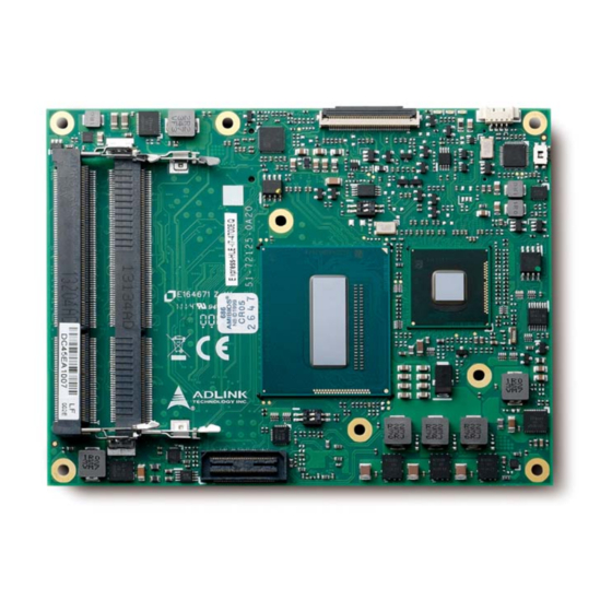
- Page 1 Express-HLE User’s Manual Manual Revision: 1.01 Revision Date: October 22, 2014 Part Number: 50-1J050-1010...
-
Page 2: Revision History
Revision History Revision Description Date 1.00 Initial release 2014-04-23 1.01 Add BIOS beep codes; correct PCIe Configuration Switch settings 2014-10-22 Page 2 Express-HLE... -
Page 3: Preface
Preface Copyright 2014 ADLINK Technology, Inc. This document contains proprietary information protected by copyright. All rights are reserved. No part of this manual may be reproduced by any mechanical, electronic, or other means in any form without prior written permission of the manufacturer. -
Page 4: Table Of Contents
Table of Contents Revision History ......................2 Preface..........................3 Introduction ......................6 Specifications ......................7 Core System ..........................7 Expansion Busses ..........................7 Video .............................7 Audio.............................8 LAN..............................8 Multi I/O and Storage ........................8 TPM (Trusted Platform Module)....................8 SEMA Board Controller .........................8 Debug............................8 2.10 Power Specifications .........................9 2.11 Operating Temperatures......................9... - Page 5 Smart Embedded Management Agent (SEMA) ..........40 Board Specific SEMA Functions ....................41 System Resources ....................43 System Memory Map......................... 43 Direct Memory Access Channels ....................43 I/O Map............................44 Interrupt Request (IRQ) Lines ....................46 PCI Configuration Space Map ....................48 PCI Interrupt Routing Map......................
-
Page 6: Introduction
1 Introduction The Express-HLE is a COM Express® COM.0 R2.1 Type 6 module supporting the 64-bit 4th Generation Intel® Core™ i7/i5/3 processor with Intel® QM87 Chipset and 4th Generation Intel® Celeron® processor with Intel® HM86 Chipset. The Express-HLE is specifically designed for customers who need high-level processing and graphics performance in a long product life solution. -
Page 7: Specifications
2 Specifications 2.1 Core System CPU: 4th Generation Intel® Core™ and Celeron® Processors - 22nm, (formerly known as "Haswell Platform") • Intel® Core™ i7-4860EQ 2.4 GHz (3.2 GHz Turbo), 47W (4C/GT3) • Intel® Core™ i7-4700EQ 2.4/1.7 GHz (3.4 GHz Turbo), 47/37W (4C/GT2) •... -
Page 8: Audio
2.4 Audio Integrated: Intel® HD Audio integrated in PCH QM87/QM86 Audio Codec: Realtek ALC886 on Express-BASE6 2.5 LAN Integrated: LAN MAC integrated in PCH QM87/HM86 Intel PHY: Intel® Ethernet Controller i217LM Interface: 10/100/1000 GbE connection 2.6 Multi I/O and Storage Integrated in Intel®... -
Page 9: Power Specifications
2.10 Power Specifications Power Modes: AT and ATX mode (AT mode start controlled by SEMA) Standard Voltage Input: ATX = 12V±5% / 5Vsb ±5% or AT = 12V ±5% Wide Voltage Input: ATX = 8.5~20 V / 5Vsb ±5% or AT = 8.5 ~20V Power Management: ACPI 4.0 compliant, Smart Battery support Power States: supports C1-C6, S0, S1, S4, S3, S5, S5 ECO mode (Wake on USB S3/S4, WOL S3/S4/S5) 2.11... -
Page 10: Function Diagram
2.15 Function Diagram 1333/1600 MHz 60-pin 1~8 GB DDR3L 1333/1600 MHz DDI 2 (port C) 1~8 GB DDR3L DP / HDMI / DVI DDI 3 (port D) single / dual DP / HDMI / DVI 18/24-bit LVDS RTD2136R 2 lane “Haswell”... -
Page 11: Mechanical Drawing
2.16 Mechanical Drawing Express-HLE Page 11... -
Page 12: Pinouts And Signal Descriptions
3 Pinouts and Signal Descriptions 3.1 AB / CD Pin Definitions The Express-HLE is a Type 6 module supporting USB3.0 and DDI channels on the CD connector All pins in the COM Express specification are described, including those not supported on the Express-HLE. Those not supported on the Express-HLE module are crossed out Row A Row B... - Page 13 Row A Row B Row C Row D Name Name Name Name USB6- USB7- DDI1_PAIR3+ DDI3_CTRLCLK_AUX+ USB6+ USB7+ DDI1_PAIR3- DDI3_CTRLDATA_AUX- USB_6_7_OC# USB_4_5_OC# RSVD DDI3_DDC_AUX_SEL USB4- USB5- DDI3_PAIR0+ DDI2_PAIR0+ USB4+ USB5+ DDI3_PAIR0- DDI2_PAIR0- GND (FIXED) GND (FIXED) GND (FIXED) GND (FIXED) USB2- USB3- DDI3_PAIR1+...
- Page 14 Row A Row B Row C Row D Name Name Name Name LVDS_A_CK+ LVDS_B_CK+ PEG_RX9+ PEG_TX9+ LVDS_A_CK- LVDS_B_CK- PEG_RX9- PEG_TX9- LVDS_I2C_CK LVDS_BKLT_CTRL TPM_PP RSVD LVDS_I2C_DAT VCC_5V_SBY GPI3 VCC_5V_SBY PEG_RX10+ PEG_TX10+ RSVD VCC_5V_SBY PEG_RX10- PEG_TX10- RSVD VCC_5V_SBY PCIE0_CK_REF+ BIOS_DIS1# PEG_RX11+ PEG_TX11+ PCIE0_CK_REF- VGA_RED PEG_RX11-...
-
Page 15: Signal Description Terminology
3.2 Signal Description Terminology The following terms are used in the COM Express AB/CD Signal Descriptions below. Input to the Module Output from the Module Bi-directional input / output signal Open drain output I 3.3V Input 3.3V tolerant I 5V Input 5V tolerant O 3.3V Output 3.3V signal level... -
Page 16: Ab Signal Descriptions
3.3 AB Signal Descriptions 3.3.1 Audio Signals Signal Pin # Description PU/PD Comment AC_RST# / Reset output to codec, active low. O 3.3VSB VSB because PCH uses suspend HDA_RST# power for RESET AC_SYNC / Sample-synchronization signal to the codec(s). O 3.3V HDA_SYNC AC_BITCLK / Serial data clock generated by the external... - Page 17 3.3.3 LVDS Signal Pin # Description PU/PD Comment LVDS_A0+ LVDS Channel A differential pairs O LVDS LVDS_A0- LVDS_A1+ LVDS_A1- LVDS_A2+ LVDS_A2- LVDS_A3+ LVDS_A3- LVDS_A_CK+ LVDS Channel A differential clock O LVDS LVDS_A_CK- LVDS_B0+ LVDS Channel B differential pairs O LVDS LVDS_B0- LVDS_B1+ LVDS_B1-...
- Page 18 3.3.5 Serial ATA Signal Pin # Description PU/PD Comment SATA0_TX+ Serial ATA channel 0, Transmit Output O SATA AC coupled on Module SATA0_TX- differential pair. SATA0_RX+ Serial ATA channel 0, Receive Input I SATA AC coupled on Module SATA0_RX- differential pair. SATA1_TX+ Serial ATA channel 1, Transmit Output O SATA...
- Page 19 3.3.6 PCI Express Signal Pin # Description PU/PD Comment PCIE_TX0+ PCI Express channel 0, Transmit Output differential O PCIE AC coupled on Module PCIE_TX0- pair. PCIE_RX0+ PCI Express channel 0, Receive Input differential I PCIE AC coupled off Module PCIE_RX0- pair.
- Page 20 3.3.9 Signal Pin # Description PU/PD Comment USB0+ USB differential data pairs for Port 0 I/O 3.3VSB USB 1.1/ 2.0 compliant USB0- USB1+ USB differential data pairs for Port 1 I/O 3.3VSB USB 1.1/ 2.0 compliant USB1- USB2+ USB differential data pairs for Port 1 I/O 3.3VSB USB 1.1/ 2.0 compliant USB2-...
- Page 21 3.3.10 USB Root Segmentation Express-HLE Page 21...
- Page 22 3.3.11 SPI (BIOS only) Signal Pin # Description PU/PD Comment SPI_CS# Chip select for Carrier Board SPI BIOS Flash. O 3.3VSB SPI_MISO Data in to module from carrier board SPI BIOS flash. I 3.3VSB SPI_MOSI Data out from module to carrier board SPI BIOS flash. O 3.3VSB SPI_CLK Clock from module to carrier board SPI BIOS flash.
- Page 23 3.3.14 I2C Bus Signal Pin # Description PU/PD Comment I2C_CK General purpose I²C port clock output/input I/O OD 3.3VSB PU 2k2 3.3VSB I2C_DAT General purpose I²C port data I/O line I/O OD 3.3VSB PU 2k2 3.3VSB 3.3.15 General Purpose I/O (GPIO) Signal Pin # Description...
- Page 24 3.3.17 Power And System Management Signal Pin # Description PU/PD Comment PWRBTN# Power button to bring system out of S5 (soft off), active on falling edge. I 3.3VSB PU 10k 3.3VSB SYS_RESET# Reset button input. Active low request for module to reset and reboot. May I 3.3VSB PU 10k be falling edge sensitive.
-
Page 25: Cd Signal Descriptions
3.4 CD Signal Descriptions 3.4.1 USB 3.0 extension Signal Description PU/PD Comment USB_SSRX0- Additional Receive signal differential pairs for the I PCIE USB_SSRX0+ SuperSpeed USB data path on USB0 USB_SSTX0- Additional Transmit signal differential pairs for the O PCIE AC coupled on Module USB_SSTX0+ SuperSpeed USB data path on USB0 USB_SSRX1-... - Page 26 3.4.3 DDI Channels DDI 1 Signal Description PU/PD Comment DDI1_PAIR0+ Digital Display Interface1 differential pairs O PCIE DDI1_PAIR0- DDI1_PAIR1+ DDI1_PAIR1- DDI1_PAIR2+ DDI1_PAIR2- DDI1_PAIR3+ DDI1_PAIR3- DDI1_PAIR4+ Pair 4 to Pair 6 DDI1_PAIR4- Not supported DDI1_PAIR5+ DDI1_PAIR5- DDI1_PAIR6+ DDI1_PAIR6- DDI1_HPD Digital Display Interface Hot-Plug Detect I PCIE DDI1_CTRLCLK_AUX+ IF DDI1_DDC_AUX_SEL is floating...
- Page 27 DDI 2 Signal Description PU/PD Comment DDI2_PAIR0+ Digital Display Interface2 differential pairs DDI2_PAIR0- DDI2_PAIR1+ DDI2_PAIR1- DDI2_PAIR2+ DDI2_PAIR2- DDI2_PAIR3+ DDI2_PAIR3- DDI2_HPD DDI2_CTRLCLK_AUX+ IF DDI2_DDC_AUX_SEL is floating I/O PCIe DP2_AUX+ IF DDI2_DDC_AUX_SEL pulled high I/O OD 3.3V HDMI2_CTRLCLK DDI2_CTRLCLK_AUX- IF DDI2_DDC_AUX_SEL is floating I/O PCIe DP2_AUX+ IF DDI2_DDC_AUX_SEL pulled high...
- Page 28 3.4.4 DDI to DP/HDMI Mapping Pin Name HDMI / DVI DDI1_PAIR0+ DP1_LANE0+ TMDS1_DATA2+ DDI1_PAIR0- DP1_LANE0- TMDS1_DATA2- DDI1_PAIR1+ DP1_LANE1+ TMDS1_DATA1+ DDI1_PAIR1- DP1_LANE1- TMDS1_DATA1- DDI1_PAIR2+ DP1_LANE2+ TMDS1_DATA0+ DDI1_PAIR2- DP1_LANE2- TMDS1_DATA0- DDI1_PAIR3+ DP1_LANE3+ TMDS1_CLK+ DDI1_PAIR3- DP1_LANE3- TMDS1_CLK- DDI1_PAIR4+ Not supported Not supported DDI1_PAIR4- Not supported Not supported DDI1_PAIR5+...
- Page 29 3.4.5 PCI Express Graphics x16 (PEG) Signal Description PU/PD Comment PEG_RX0+ PCI Express Graphics transmit differential pairs. I PCIE AC coupled on Module PEG_RX0- PEG_RX1+ PEG_RX1- PEG_RX2+ PEG_RX2- PEG_RX3+ PEG_RX3- PEG_RX4+ PEG_RX4- PEG_RX5+ PEG_RX5- PEG_RX6+ PEG_RX6- PEG_RX7+ PEG_RX7- PEG_RX8+ PEG_RX8- PEG_RX9+ PEG_RX9- PEG_RX10+...
- Page 30 Signal Description PU/PD Comment PEG_TX15+ D101 PEG_TX15- D102 PEG_LANE_RV# PCI Express Graphics lane reversal input strap. I 1.05V Pull low on the Carrier board to reverse lane order. 3.4.6 Module Type Definition Signal Pin # Description Comment TYPE0# The TYPE pins indicate to the Carrier Board the Pin-out Type that is implemented on Type 6 TYPE1# the module.
-
Page 31: Connector Pinouts On Module
4 Connector Pinouts on Module This chapter describes connectors and pinouts, LEDs and switches that are used on the module but are not included in the PICMG standard specification Connector and LED Locations XDP 60-pin to CPU BIOS Defaults RESET Button 40-pin 4-pin... -
Page 32: 40-Pin Debug Connector
4.1 40-pin Debug Connector FPC Connector type: FCI 59GF Flex 10042867 Pin orientation Express-HLE and the Debug Module Page 32 Express-HLE... - Page 33 40-pin Pin Description on the COM Express Module Interface Signal Remark Pin Interface Signal Remark VCC_SPI_IN SPI Power Input from flash tool BMC Program TXD6 Program to module. HW need add MOS interface interface FET to switch SPI power for SPI (continued) RXD6 SPI_BIOS_CS0#...
-
Page 34: Status Leds
4.2 Status LEDs To facilitate easier maintenance, status LED’s are mounted on the board. LED Descriptions Name Color Connection Function LED1 Blue BMC output Power Sequence Status Code (BMC) Power Changes, RESET (see 5.1.4 Exception Codes below) LED2 Green Power Source 3Vcc LED ON S3/S4/S5 LED OFF... -
Page 35: Xdp Debug Header
4.3 XDP Debug header The debug port is a connection into a target-system environment that provides access to JTAG, run control, system control, and observation resources. The XDP target system connector is a Samtec™ 60-pin BSH-030-01 series connector. Pin XDP Signal Target Signal Device Pin XDP Signal... -
Page 36: Fan Connector
4.4 Fan Connector Connector Type: JVE 24W1125A-04M00 Pin Assignment Name Signal Description BMC_FAN_OUT FAN_PWMOUT BMC_FAN_PWM_IN FAN_TACHIN Ground P5V_S 4.5 BIOS Setup Defaults RESET Button To perform a hardware reset of BIOS default settings, perform the following steps: Shut down the system. Press the BIOS Setup Defaults RESET Button continuously and boot up the system. -
Page 37: Express-Hle Switch Settings
4.6 Express-HLE Switch Settings 4.6.1 Switch Locations Express-HLE Page 37... - Page 38 4.6.2 SW1: PCI Express Configuration Switch Switch SW1 allows you to configure the PCI Express x16 lanes from the CPU as 1 PCIe x16, 2 PCIe x8, or 1 PCIe x8 + 2 PCIe x4. Mode Pin 1 Pin 2 1x PCIe x16 (default) 2x PCIe x8 1x PCIe x8 + 2x PCIe x4...
-
Page 39: Pcie X16-To-Two-X8 Adapter Card
4.7 PCIe x16-to-two-x8 Adapter Card The Express-HLE can be used with the PCIe x16-to-two-x8 Adapter Card on the Express-BASE6 Reference Carrier to support bifurbication of the CPU's PEG interface (PCIe x16). The card reroutes the PCIe x16 to two x8 and allows testing of two independent PCIe add-on cards with x8/x4/x2/x1 width. -
Page 40: Smart Embedded Management Agent (Sema)
5 Smart Embedded Management Agent (SEMA) The onboard microcontroller (BMC) implements power sequencing and Smart Embedded Management Agent (SEMA) functionality. The microcontroller communicates via the System Management Bus with the CPU/chipset. The following functions are implemented: • Total operating hours counter. Counts the number of hours the module has been run in minutes. •... -
Page 41: Board Specific Sema Functions
5.1 Board Specific SEMA Functions 5.1.1 Voltages The BMC of the Express-HLE implements a voltage monitor and samples several onboard voltages. The voltages can be read by calling the SEMA function “Get Voltages”. The function returns a 16-bit value divided into high-byte (MSB) and low-byte (LSB). ADC Channel Voltage Name Voltage Formula [V]... - Page 42 5.1.4 Exception Codes In case of an error, the BMC drives a blinking code on the blue Status LED (LED1). The same error code is also reported by the BMC Flags register. The Exception Code is not stored in the Flash Storage and is cleared when the power is removed. Therefore, a “Clear Exception Code”...
-
Page 43: System Resources
6 System Resources 6.1 System Memory Map Address Range (decimal) Address Range (hex) Size Description (4GB-2MB) FFE00000 – FFFFFFFF 2 MB High BIOS Area (4GB-18MB) – (4GB-17MB-1) FEE00000 – FEEFFFFF 1 MB MSI Interrupts (4GB-20MB) – (4GB-19MB-1) FEC00000 – FECFFFFF 1 MB APIC Configuration Space 15MB –... -
Page 44: I/O Map
6.3 I/O Map Hex Range Device 000-01F DMA controller 1, 8237A-5 equivalent 020-02D and 030-03F Interrupt controller 1, 8259 equivalent 02E-02F LPC SIO () configuration index/data registers 040-05F Timer, 8254-2 equivalent 060, 062, 064, 066, 068-06F 8742 equivalent (keyboard) 061, 063, 065, 067 NMI control and status 070-07F Real Time Clock Controller( bit 7 -NMI mask) - Page 45 I/O Map (cont'd) Hex Range Device 3BC-3BE Reserved for parallel port 3C0-3DF VGA registers 3E0-3EF Available 3F0-3F7 Available 3F8-3FF Serial port 1 Master PIC Edge/Level Trigger register Slave PIC Edge/Level Trigger register CF8-CFB PCI configuration address register (32 bit I/O only) Reset Control register (8 bit I/O) CFC-CFF PCI configuration data register...
-
Page 46: Interrupt Request (Irq) Lines
6.4 Interrupt Request (IRQ) Lines PIC Mode IRQ# Typical Intterupt Resource Connected to Pin Available Counter 0 Keyboard controller Cascade interrupt from slave PIC Serial Port 2 (COM2) / PCI IRQ3 via SERIRQ / PIRQ Note (1) Serial Port 1 (COM1) / PCI IRQ4 via SERIRQ / PIRQ Note (1) Parallel Port 2 (LPT2) - Page 47 APIC Mode (cont'd) IRQ# Typical Intterupt Resource Connected to Pin Available Intel HDA, PCIE Port 0/1/2/3/4/5/6, EHCI Conterller Note (1) #2 ,P.E.G Root Port, I.G.D ,XHCI Controller PCIE Port 0/1/2/3/4/5/6, P.E.G Root Port, Note (1) PCIE Port 0/1/2/3/4/5/6, P.E.G Root Port, SMBus Note (1) Controller, EHCI Controller #2 PCIE Port 0/1/2/3/4/5/6, P.E.G Root Port,...
-
Page 48: Pci Configuration Space Map
6.5 PCI Configuration Space Map Device Function Routing Description Number Number Number Intel host Bridge Internal Intel I.G.D Internal HD Audio Device Internal xHCI Controller Internal Intel Management Engine Interfaxe #1 Internal Intel Management Engine Interfaxe #2 Internal IDE-R Internal Internal Gigabit Etherent Controller Internal... -
Page 49: Pci Interrupt Routing Map
6.6 PCI Interrupt Routing Map P.E.G Audio xHCI IDE-R GbEt Line Root Port Controller Controller Controller #1 Controller #2 Controller Controller Int0 INTA:16 INTA:16 INTA:21 INTA:16 INTE:20 INTG:22 Int1 INTD:19 Int2 INTC:18 Int3 INTB:17 PCIE port1 PCIE port 2 PCIE port 3 PCIE port 4 PCIE Port 5 PCIE Port 6 PCIE Port 7 PCIE port 8... -
Page 50: Bios Setup
7 BIOS Setup 7.1 Menu Structure This section presents the six primary menus of the BIOS Setup Utility. Use the following table as a quick reference for the contents of the BIOS Setup Utility. The subsections in this section describe the submenus and setting options for each menu item. The default setting options are presented in bold, and the function of each setting is described in the right hand column of the respective table. -
Page 51: Main
7.2 Main The Main Menu provides read-only information about your system and also allows you to set the System Date and Time. Refer to the tables below the screen shot of this menu for details of the submenus and settings. 7.2.1 System Information Feature... - Page 52 7.2.3.1 PCH Information System Management Feature Options Description System Management Info only Version Info only Display version. 7.2.4 System Management 7.2.4.1 System Management > Board Information Board Information Info only SMC Firmware Read only Display SMC Firmware. Build Date Read only Display SMC firmware build date.
- Page 53 7.2.4.3 System Management > Power Consumption Feature Options Description Power Consumption Info only Current Input Current Read only Display input current. Current Input Power Read only Display input power. AIN0 Read only Display actual voltage of the AIN0. V3.30 Read only Display actual voltage of the V3.30.
- Page 54 7.2.4.6 System Management > Power Up Feature Options Description Power Up Info only Power Up watchdog Enabled The Power-Up Watchdog resets the system after a certain Disabled amount of time after power-up. Attention: F12 disables the Power Up Watchdog. ECO Mode Disabled Reduces the power consumption of the system.
- Page 55 7.2.5 System Date and Time Feature Options Description System Date Weekday, MM/DD/YYYY Requires the alpha-numeric entry of the day of the week, day of the month, calendar month, and all 4 digits of the year, indicating the century and year (Fri XX/XX/20XX) System Time HH/MM/SS Presented as a 24-hour clock setting in hours, minutes, and seconds...
-
Page 56: Advanced
7.3 Advanced This menu contains the settings for most of the user interfaces in the system 7.3.1 Feature Options Description Info only Manufacturer, model, speed CPU Signature Info only Display CPU Signature. Processor Family Info only Display Processor Family. Microcode Patch Info only Display Microcode Patch. - Page 57 Feature Options Description CPU C3 Report Disabled Enable/Disable CPU C3 report to OS. Enabled CPU C6 Report Disabled Enable/Disable CPU C6 report to OS. Enabled CPU C7 Report Disabled Enable/Disable CPU C7 report to OS. CPU C7 CPU C7S ACPI T State Disabled Enable/Disable ACPI T state support.
- Page 58 7.3.3 Graphics Feature Options Description Graphics Configuration Info only IGFX VBIOS Version Info only Display VBIOS Version. IGfx Frequency Info only Display IGfx Frequency. Graphics Turbo IMON Current Number entry field Graphics turbo IMON current values supported (14-31). Primary Display Auto Select which of IGFX/PEG/PCI Graphics device should be Primary Display Or select SG for Switchable Gfx.
- Page 59 Feature Options Description LCD Panel Type VBIOS Default Select LCD panel used by Internal Graphics Device by selecting the appropriate setup item. 640X480 800X600 1024X768 1280X1024 1400X1050 1600X1200 1366X768 1680X1050 1920X1200 1440X900 1600X900 1024X768 LVDS2 1280X800 1920X1080 2048X1536 Active LFP No LVDS Select the Active LFP Configuration.
- Page 60 Feature Options Description Software Feature Mask Configuration Info only RAID0 Enabled Enable/Disable RAID0 feature. Disabled RAID1 Enabled Enable/Disable RAID1 feature. Disabled RAID10 Enabled Enable/Disable RAID10 feature. Disabled RAID5 Enabled Enable/Disable RAID5 feature. Disabled Intel Rapid Recovery Technology Enabled Enable/Disable Intel Rapid Recovery Technology. Disabled OROM UI and BANNER Enabled...
- Page 61 Feature Options Description Hot Plug Disabled Designates this port as Hot Pluggable. Enabled Mechanical Presence Disabled Controls reporting if this port has an Mechanical Presence Switch.\n\nNote: Requires hardware support. Enabled External SATA Disabled External SATA Support. Enabled SATA Device Type Hard Disk Drive Identify the SATA port is connected to Solid State Drive or Hard Disk Drive.
- Page 62 7.3.5.1 USB > PCH USB Configuration Feature Options Description USB Precondition Disabled Precondition work on USB host controller and root ports for faster enumeration. Enabled XHCI Mode Disabled Mode of operation of xHCI controller. Enabled BTCG Disabled Enable/Disable trunk clock gating. Enable USB Precondition Disabled...
- Page 63 Feature Options Description PET Progress Enabled User can Enable/Disable PET Events progress to recieve PET Disabled events or not. AMT CIRA Timeout OEM defined timeout for MPS connection to be established. 0 - use the default timeout value of 60 seconds. 255 - MEBX waits until the connection succeeds.
- Page 64 Feature Options Description Extended Synch Enabled If enabled the generation of PCI Express synchronization patterns is Disabled allowed Link Training Retry Disabled Defines number of Retry Attempts software will take to retrain the link if previous training attempt was unsuccessful. Link Training Timeout (uS) Defines number of microseconds software will wait before polling 'Link Training' bit in Link Status register.
- Page 65 Feature Options Description Disable PEG RxCEM LoopBack Mode Disabled Enabled/Disabled PEG RxCEM Loopback Mode. Enable PCIe Gen3 RxCTLEp Setting 0~7 The range of the setting is (0~15) This setting has to be specified basing on platform design and following the guideline. 7.3.7.2 PCI and PCIe >...
- Page 66 Feature Options Description Disabled Enable/Disable PCI Express Device Correctable Error Reporting. Enable Disabled Enable/Disable PCI Express Completion Timer TO. Enable SEFE Disabled Enable/Disable Root PCI Express System Error on Fatal Error. Enable SENFE Disabled Enable/Disable Root PCI Express System Error on Non- Fatal Error.
- Page 67 Feature Options Description Auto Change Settings IO=3F8h; IRQ=4 Select an optimal setting for Super IO device. IO=3F8h; IRQ=3,4,5,6,7,10,11,12 IO=2F8h; IRQ=3,4,5,6,7,10,11,12 IO=3E8h; IRQ=3,4,5,6,7,10,11,12 IO=2E8h; IRQ=3,4,5,6,7,10,11,12 Serial Port 2 Configuration Serial Port Enabled Enable/Disable Serial Port (COM). Disabled IO=2F8h; IRQ=4 Device Settings Fixed configuration of serial port.
- Page 68 7.3.9 ACPI and Power Management Feature Options Description ACPI and Power Management Info only Enable ACPI Auto Configuration Enabled Enables or Disables BIOS ACPI Auto Configuration. Disabled Enable Hibernation Enabled Enables or Disables System ability to Hibernate (OS/S4 Sleep Disabled State).
- Page 69 7.3.11.1 Serial Port Console > Console Redirection Settings Feature Options Description Console Redirection Settings Info only Terminal Type VT100 Emulation: ANSI: Extended ASCII char set. VT100: ASCII char set. VT100+: Extends VT100 to support color, function keys, VT100+ etc. VT-UTF8: Uses UTF8 encoding to map Unicode chars onto VT-UTF8 1 or more bytes.
- Page 70 Feature Options Description Turn off unused PCI/PCIe clocks Disabled Disabled: all clocks turned on. Enable Enabled: clocks for empty PCI/PCIe slots will be turned off to save power. Platform must be powered off for changes to take effect. ICC Locks After EOP Default Lock ICC register after EOP.
- Page 71 Feature Options Description Trusted Computing Submenu Intel TXT(LT) Configuration Enabled Enables or Disables the High Precision Event Timer. Disabled 7.3.14.1 Miscellaneous > BIOS Security Configuration Feature Options Description SMI Lock Enabled Enable or Disable the SMI Lock Disabled BIOS Lock Enabled Enable or Disable the BIOS lock enable (BLE) bit Disabled...
-
Page 72: Boot
7.4 Boot 7.4.1 Boot Configuration Feature Options Description Boot Configuration Info only Setup Prompt Timeout Enable/Disable the onboard SATA controllers. Bootup NumLock State Select SATA controller mode. Quiet Boot Disabled Enable/Disable the PATA port. In fact this enables or disables the SATA channel on which the onboard SATA to PATA converter is Enabled attached. -
Page 73: Security
7.5 Security 7.5.1 Password Description Feature Options Description Administrator Password Enter password User Password Enter password Secure Boot menu Submenu 7.5.2 Secure Boot Menu Feature Options Description System Mode Setup Secure Boot Info only Secure Boot Support Disabled Secure Boot can be enabled if 1.System running in User mode with enrolled Platform Key(PK) 2.CSM function is disabled. -
Page 74: Bios Checkpoints, Beep Codes
8 BIOS Checkpoints, Beep Codes This section of this document lists checkpoints and beep codes generated by AMI Aptio BIOS. The checkpoints defined in this document are inherent to the AMIBIOS generic core, and do not include any chipset or board specific checkpoint definitions. Checkpoints and Beep Codes Definition A checkpoint is either a byte or word value output to I/O port 80h. -
Page 75: Status Code Ranges
Status Code Ranges Status Code Description Range 0x01 – 0x0F SEC Status Codes & Errors 0x10 – 0x2F PEI execution up to and including memory detection 0x30 – 0x4F PEI execution after memory detection 0x50 – 0x5F PEI errors 0x60 – 0xCF DXE execution up to BDS 0xD0 –... - Page 76 8.2.2 SEC Beep Codes None 8.2.3 PEI Status Codes Status Code Description Progress Codes 0x10 PEI Core is started 0x11 Pre-memory CPU initialization is started 0x12 Pre-memory CPU initialization (CPU module specific) 0x13 Pre-memory CPU initialization (CPU module specific) 0x14 Pre-memory CPU initialization (CPU module specific) 0x15 Pre-memory North Bridge initialization is started...
- Page 77 Status Code Description 0x4F DXE IPL is started PEI Error Codes 0x50 Memory initialization error. Invalid memory type or incompatible memory speed 0x51 Memory initialization error. SPD reading has failed 0x52 Memory initialization error. Invalid memory size or memory modules do not match. 0x53 Memory initialization error.
- Page 78 8.2.4 PEI Beep Codes # of Beeps Description Memory not Installed Memory was installed twice (InstallPeiMemory routine in PEI Core called twice) Recovery started DXEIPL was not found DXE Core Firmware Volume was not found Reset PPI is not available Recovery failed S3 Resume failed 8.2.5...
- Page 79 Status Code Description 0x77 South Bridge DXE Initialization (South Bridge module specific) 0x78 ACPI module initialization 0x79 CSM initialization 0x7A – 0x7F Reserved for future AMI DXE codes 0x80 – 0x8F OEM DXE initialization codes 0x90 Boot Device Selection (BDS) phase is started 0x91 Driver connecting is started 0x92...
- Page 80 Status Code Description 0xAF Exit Boot Services event 0xB0 Runtime Set Virtual Address MAP Begin 0xB1 Runtime Set Virtual Address MAP End 0xB2 Legacy Option ROM Initialization 0xB3 System Reset 0xB4 USB hot plug 0xB5 PCI bus hot plug 0xB6 Clean-up of NVRAM 0xB7 Configuration Reset (reset of NVRAM settings)
-
Page 81: Oem-Reserved Checkpoint Ranges
8.2.7 ACPI/ASL Checkpoint Status Code Description 0x01 System is entering S1 sleep state 0x02 System is entering S2 sleep state 0x03 System is entering S3 sleep state 0x04 System is entering S4 sleep state 0x05 System is entering S5 sleep state 0x10 System is waking up from the S1 sleep state 0x20... -
Page 82: Mechanical Information
9 Mechanical Information 9.1 Board-to-Board Connectors To allow for different stacking heights, the receptacles for COM Express carrier boards are available in two heights: 5 mm and 8 mm. When 5 mm receptacles are chosen, the carrier board should be free of components. Tyco 3-1827253-6 Foxconn QT002206-2131-3H •... -
Page 83: Thermal Solution
9.2 Thermal Solution 9.2.1 Heat Spreaders The function of the heat spreader is to ensure an identical mechanical profile for all COM Express modules. By using a heat spreader, the thermal solution that is built on top of the module is compatible with all COM Express modules. 9.2.2 Heat Sinks A heat sink can be used as a thermal solution for a specific COM Express module and can have a fan or be fanless, depending on the... - Page 84 Step 4: Use the four M2.5, L=6mm screws provided to fasten the heatsink to the module. Step 5: Place the COM Express module and heatsink assembly onto the connectors on the carrier board as shown. Then press down on the module until it is firmly seated on the carrier board. Step 6: Use the five M2.5, L=16mm screws provided to secure the COM Express module to the carrier board from the solder side.
-
Page 85: Mounting Methods
9.3 Mounting Methods There are several standard ways to mount the COM Express module with a thermal solution onto a carrier board. In addition to the choice of 5 mm or 8mm board-to-board connectors, there is the choice of Top and Bottom mounting. In Top mounting, the threaded standoffs are on the carrier board and the thermal solution is equipped with through-hole standoffs. -
Page 86: Standoff Types
9.4 Standoff Types The standoffs available for Top and Bottom mounting methods are shown below. Note that threaded standoffs are DIP type and through- hole standoffs are SMT type. Other types not listed are available upon request. 5mm through-hole standoff (SMT type) 5mm threaded standoff (DIP type) P/N: 33-72000-0050 P/N: 33-72016-0050... -
Page 87: Safety Instructions
Safety Instructions Read and follow all instructions marked on the product and in the documentation before you operate your system. Retain all safety and operating instructions for future use. • Please read these safety instructions carefully. • Please keep this User‘s Manual for later reference. •... -
Page 88: Getting Service
5215 Hellyer Avenue, #110, San Jose, CA 95138, USA Tel: +1-408-360-0200 Toll Free: +1-800-966-5200 (USA only) Fax: +1-408-360-0222 Email: info@adlinktech.com ADLINK Technology (China) Co., Ltd. Address: 300 Fang Chun Rd., Zhangjiang Hi-Tech Park,Pudong New Area Shanghai, 201203 China Tel: +86-21-5132-8988 Fax: +86-21-5132-3588 Email: market@adlinktech.com... - Page 89 84 Genting Lane #07-02A, Cityneon Design Centre Singapore 349584 Tel: +65-6844-2261 Fax: +65-6844-2263 Email: singapore@adlinktech.com ADLINK Technology Singapore Pte. Ltd. (Indian Liaison Office) Address: #50-56, First Floor, Spearhead Towers Margosa Main Road (between 16th/17th Cross), Malleswaram Bangalore - 560 055, India Tel: +91-80-65605817, +91-80-42246107 Fax:...
Need help?
Do you have a question about the COM Express Express-HLE and is the answer not in the manual?
Questions and answers