Table of Contents
Advertisement
Quick Links
Advertisement
Table of Contents

Related Manuals for ICOP Technology ICOP-602X


Summary of Contents for ICOP Technology ICOP-602X
- Page 1 ICOP-602X Embedded 386SX CPU ISA Half Size SBC User’s Manual...
- Page 2 Copyright Notice This document is copyrighted, 2000 by ICOP Technology Inc. All rights are reserved. The information in the manual is subject to change without notice in order to improving products. No part of this manual may be reproduced, copied, translated or transmitted in any form or by any means without the prior written permission of the manufacturer.
-
Page 3: Table Of Contents
T a b l e o f C o n t e n t s Chapter 0 S t a r t u p 0 . 1 P a c k i n g L i s t ........1 0 . - Page 4 3 . 5 A u t o - D e t e c t H a r d D i s k s ......3 9 3 .
-
Page 5: Startup
C h a p t e r 0 Startup Packing List Product Function Package Name l ICOP-6025 Embedded 386SX CPU SBC l User’s Manual x 1 Embedded l Utility and Drivers Diskette x 1 386SX Half Size l FDD cable x 1 All-in-One SBC l HDD cable x 1 ICOP-6025... - Page 6 Product Function Package Name l ICOP-6024 Embedded 386SX CPU SBC l User’s Manual x 1 Embedded l Utility and Drivers Diskette x 1 386SX Half Size l FDD cable x 1 All-in-One SBC l HDD cable x 1 ICOP-6024 l RS232 cable x 1 l Printer cable with bracket x 1 l AT KB / PS2 Mouse Y-cable x 1 l ICOP-6024V Embedded 386SX CPU...
- Page 7 Product Function Package Name l ICOP-6020 Embedded 386SX CPU SBC l User’s Manual x 1 Embedded l Utility and Drivers Diskette x 1 386SX Half Size l FDD cable x 1 All-in-One SBC l HDD cable x 1 ICOP-6020 l Printer cable with bracket x 1 l AT KB / PS2 Mouse Y-cable x 1 l ICOP-6022 Embedded 386SX CPU SBC l User’s Manual x 1...
-
Page 8: Specifications
Specifications Features ICOP-6025 ICOP-6025V DM&P(Ali) M6117D Processor DM&P(Ali) M6117D Chipset Ali 5113 Multi I/O Chip AMI BIOS BIOS From 30.5ìs to 512 seconds Watchdog Timer ISA and PC/104 standard compliant Bus Interface 4MB On-Board up to 20MB Memory Memory Sockets DiskOnChip Sockets 16 Bit Digital I/O... - Page 9 Features ICOP-6024 ICOP-6024V DM&P(Ali) M6117D Processor DM&P(Ali) M6117D Chipset Ali 5113 Multi I/O Chip AMI BIOS BIOS From 30.5ìs to 512 seconds Watchdog Timer ISA and PC/104 standard compliant Bus Interface 4MB On-Board up to 20MB Memory Memory Sockets DiskOnChip Flah Disk Sockets VGA/LCD DISPLAY...
- Page 10 Features ICOP-6020 ICOP-6022 DM&P(Ali) M6117D Processor DM&P(Ali) M6117D Chipset Ali 5113 Multi I/O Chip AMI BIOS BIOS From 30.5ìs to 512 seconds Watchdog Timer ISA and PC/104 standard compliant Bus Interface up to 32MB Memory SIMM 72 pin X 2 Memory Sockets DiskOnChip Sockets Flash Disk/ EPROM...
-
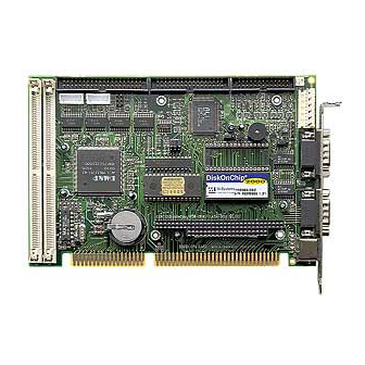
Page 11: Board Layout
Board Layout ICOP-6025 (photo A), ICOP-6025V (photo B) ICOP-6024 (photo C), ICOP-6024V (photo D) ICOP-6020 (photo E), ICOP-6022 (photo F) ICOP Embedede 386SX CPU ISA Half Size SBC User's Manual... -
Page 12: Mechanical Drawing
Mechanical Drawing ICOP-6025 (placement A), ICOP-6025V (placement B) ICOP-6024 (placement C), ICOP-6024V (placement D) ICOP-6020 (placement E), ICOP-6022 (placement F) ICOP Embedded 386SX CPU ISA Half Size SBC User's Manual... - Page 13 Enhanced IDE, High Speed I/O In addition, the ICOP-602X has one PS/2 mouse port, serial ports (RS-232 or RS485), one bidirectional printer port that supports SPP, ECP andEPP modes, an enhanced IDE HDD interface that supports PIO mode 4, and a floppy disk controller.
- Page 14 Specifications • Embedded CPU : DM&P(Ali) M6117D is an implementation of an INTEL compatible 386SX-40 CPU, Realtime clock, a watchdog timer and ALi’s M1217B chipset • BIOS : Y2K compliant AMI system BIOS • DRAM Memory: 4MB EDO DRAM onboard •...
- Page 15 enabled/disabled Environmental and Power • Power Requirements: single voltage +5 V +12V,-12V (ICOP-6020) • Board Dimensions : 185 (L) x 122 (W) mm. • Board Weight : 240 g • Extended Operating Temperature: -20~+60 °C ICOP Embedede 386SX CPU ISA Half Size SBC User's Manual...
-
Page 16: Vga Interface
VGA Interface (ICOP-6025V ,ICOP-6024V) • Chipset : HMC HM86508 • Memory : 1 MB onboard • System Bus : 16-bit ISA bus • Panel Data Bus : 24-bit • Display : CRT and Flat Panel Mono/TFT/DSTN/EL • Supported Flat Panels : NEC NL-6448AC30-10 TFT 9.4"... -
Page 17: Diskonchip 2000 Flash Disk
DiskOnChip 2000 Flash Disk Flash Disk DiskOnChip 2000 ® • Package : Single Chip FlashDisk in 32-pin DIP JEDEC • Capacity : 1-144 MByte capacity • Data Reliability : ECC/EDC error correction • Memory Window : 8 KByte ICOP Embedede 386SX CPU ISA Half Size SBC User's Manual... -
Page 18: Jumper Settings
C h a p t e r 2 Installation Jumper Settings 2.1.1 ICOP-6025/V RESET connector Power LED connector RS-232/485 selection for COM2 1-2 -> RS-232 mode (CONT11 active) 2-3 -> RS-485 mode (CONT8 active) IDE LED connector VGA IRQ9 operation (ICOP-6025V) open ->... - Page 19 Open Close Open Disabled Open Open Close Both EPROM Open Open Open Both Flash 2.1.3 ICOP-6022 RESET connector Multi I/O Ali M5113 Enable/disable 1-2 -> Enabled 2-3 -> Disabled RS-232/485 selection for COM2 1-2 -> RS-232 mode (JP4 active) 2-3 -> RS-485 mode (CONT9 active) internal COM2 RS-232 mode CONT13 DiskOnChip/EPROM Disk/Flash Disk address select DOC address...
-
Page 20: C O N N Ec T O R
Connectors 2.2.1 ICOP-6025/V CON1 External female 15-pin D-type CRT Display connector (ICOP- 6025V) CON2 Internal 44-pin Flat Panel Display connector (ICOP-6025V) CONT1 Internal 20-pin box header for 16-bit GPIO (digital I/O) CONT2 PC/104 bus 64-pin CONT3 PC/104 bus 40-pin CONT4 External PS/2 and AT keyboard connector CONT5 Speaker connector... - Page 21 CONT2 PC/104 bus 40-pin CONT3 Internal AT-keyboard connector CONT4 External PS/2 and AT keyboard connector CONT5 Internal PS/2 mouse connector CONT6 External speaker connector CONT7 Power LED connector CONT9 Internal COM2 RS-485 CONT10 FDD controller CONT11 IDE LED connector CONT12 IDE connector Parralel Port COM1 External COM1...
- Page 22 CONT12 IDE connector Parralel Port COM1 External COM1 SIM1 not available replaced by 4 MB onboard EDO memory SIM2 Memory bank 1 (FP DRAM or EDO) LED1 Power-on LED 2.2.4 ICOP-6020 CONT1 Internal 20-pin box header for 16-bit GPIO (digital I/O) CONT2 PC/104 bus 64-pin CONT3...
-
Page 23: D I S K O N C H Ip / E P R O M / F L A S H R O M D I S
2000 Flash Disk ® Installation Instructions 1. Make sure the ICOP-602X is powered OFF 2. Plug the DiskOnChip 2000 device(s) into its socket. Verify the direction is correct (pin 1 of the DiskOnChip 2000 is aligned with pin 1 of the socket) 3. -
Page 24: S E T T I N G U P A F L A S H D I S
2.3.2 Setting up a Flash Disk Before you can use the ICOP-602X’s Flash disk you will have to initialize it using a software utility called “PC104.EXE”. This program can be found on the utility disk in the subdirectory “ A:\FLASH”... -
Page 25: S E T T I N G U P A N E P R O M D I S
2.3.3 Setting up an EPROM disk EPROMs should be inserted starting from Socket. All modules have to be of the same type. To create a ROM disk you will need the following: - EPROM devices - EPROM programmer - ROM files The ROM files are hacked-up portions of your system and program files that should have the same size as your EPROM devices. - Page 26 Beware to keep track of their sequence when inserting the EPROM’s PRESS ESC KEY QUIT THIS PROGRAM ICOP Embedded 386SX CPU ISA Half Size SBC User's Manual...
-
Page 27: Watchdog Timer
Watchdog Timer The watchdog timer uses a 32.768 KHz frequency source with a 24-bit counter. Its time range stretches from 30.5 ms to 512 sec. with a resolution of 30.5 ms. When the watchdog times out a System RESET, NMI or IRQ can be invoked. - Page 28 are used to control the watchdog functions and/or display its current status. Enable/Disable watchdog - INDEX 37H Value Action reserved Do not modify the value of these bits! Disable watchdog timer Enable watchdog timer Other function Do not modify the value of these bits! Watchdog time out action - INDEX 38H Value Action...
-
Page 29: G E N E R A L P U R P O S E I
Index Bits D7……D0 D7……D0 D7……D0 counter [VSB……………. …………………... ………..LSB] For example Index Time out 30.5ìs 61ìs 7.8 ms 15.6 ms 512 s Timeout Status & Reset - INDEX 3CH Value Action Timeout has not occurred Timeout has occured Reset timer Has no meaning Other function, do not modify these bits Programming the watchdog... - Page 30 mov al, 0c5h mov al, 000h out 23h, al out 23h, al Read the value of a configuration register For example, read INDEX 3Ch : Unlock configuration register mov al, 03ch out 22h, al in al, 23h push ax Lock configuration register pop ax ;AL - result Write data to configuration register For example, write 0FFh to INDEX 3Bh :...
- Page 31 Lock configuration register Watchdog Program Example We use the following sequence to initialize the watchdog timer: (1) Unlock configuration register. (2) Disable watchdog timer by setting INDEX 37H Bit 6 to ‘0’. (3) Set the expected counter value to INDEX 3BH, 3AH, 39H. (4) Select timeout action from INDEX 38H Bit 7-4.
- Page 32 call writechip mov ax, 00039h call writechip mov ax, 03838h ; Select “system reset” as ; timeout action call readchip and al, 00001111b or al, 11010000b xchg ah, al call writechip mov ax, 03737h ; Enable watchdog timer call readchip or al, 01000000b xchg ah, al call writechip...
- Page 33 readchip endp writechip proc out 22h, al xchg ah, al out 23h, al xchg ah, al writechip endp end main Reset watchdog timer Resets the watchdog timer periodically to prevent timeout. mov ax, 0c513h ; Unlock configuration ; register call writechip mov ax, 03C3Ch ;...
- Page 34 General Purpose I/O M6117D supports 16 independent GPOs and GPIs. This group of GPOs does not need external 74LS373 to latch as generate purpose output. Also this group of GPIs do not share signals with the ISA data bus, so no external 74LS245 is required either.
- Page 35 out 23,al ; User can be set logic “0” ; of IN direction. mov al,47 ; Output data port. out 22,al mov al,55 ; Example data out value is 55, ; to output pin out 23,al ; GPIO[7-0]. So user can ;...
-
Page 36: Ami Bios Setup
C h a p t e r 3 AMI BIOS Setup When the system is powered on, the BIOS will perform diagnostics and initialize system components, including the video system. (This is self-evident when the screen first flicks before the Video Card header is displayed). -
Page 37: S T A N D A R D C M O S S E T U
Standard CMOS Setup Date The BIOS determines the day of the week from the other date information; this field is for information only. Time The time format is based on the 24-hour military-time clock. For example, 1 p.m. is 13:00:00. Press the « or ( key to move to the desired field . Press the PgUp or PgDn key to increment the setting, or type the desired value into the field. - Page 38 Type: The BIOS contains a table of predefined drive types. Each defined drive type has a specified number of cylinders, number of heads, write precompensation factor, landing zone, and number of sectors. Drives whose specifications do not accommodate any predefined type are classified as type USER.
- Page 39 own BIOS on the controller. Disabled recommended. If you want virus protection, use a TSR (Terminate and Stay Resident) virus detection (Norton, Central Point, etc ...). Scan by Macfee is also a good idea. Available on most FTP servers, it is shareware. ICOP Embedede 386SX CPU ISA Half Size SBC User's Manual...
-
Page 40: A D V A N C E D C M O S S E T U
Advanced CMOS Setup 1st Boot Device Specifies the first device for which to look and use for booting the system. Options are : Disabled 1st IDE-HDD, 2nd IDE-HDD, 3rd IDE-HDD, 4th IDE- HDD, Floppy, ARMD-FDD, ARMD-HDD, ATAPI CDROM, SCSI or NETWORK. ARMD (FDD/HDD) means “ATAPI Removeable Media Device”. - Page 41 Always The system will not boot and access to Setup will be denied if the correct password is not entered at the prompt. Setup The system will boot, but access to Setup will be denied if the correct password is not entered at the prompt. C8000, 16 K Shadow Specifies whether the specified area of ROM is to be shadowed and if shadowed, whether it should be written to or read from cache memory.
- Page 42 Advanced Chipset CMOS Setup VGA Frame Buffer Size The STPC implements a single memory subsystem for both the system as well as the frame buffer memory. In other words, the size of the DRAM available to the system is reduced by the size of the DRAM allocated to the frame buffer.
-
Page 43: P E R I P H E R A L S E T U
Peripheral Setup Onboard FDC Enable/disable or Auto detect FDD Controller Onboard Serial Port1 Disable or enable wtih I/O address 3E8h, 3F8h as COM1 or 2E8h or 2F8h as COM2 Onboard Serial Port1 Disable or enable wtih I/O address 3E8h, 3F8h as COM1 or 2E8h or 2F8h as COM2 Onboard Parallel Port This option specifies the parallel port mode. - Page 44 <I> Auto-detection BIOS setup will display all possible modes supported by the HDD including NORMAL, LBA & LARGE. If HDD does not support LBA modes, no ’LBA’ option will be shown. Users can select a mode that is appropriate for them. <II>...
- Page 45 x no. Sector x bytes per sector 512) 814 Gigabytes n LARGE mode Extended HDD access mode supported by Award Software. Some IDE HDDs contain more than 1024 cylinder without LBA support (in some cases, user does not want LBA). The Award BIOS provides another alternative to support these kinds of HDD! Example of LARGE mode: CYLS...
-
Page 46: C H A N G E S U P E R V I S O R P A S S W O R
Change Supervisor Password When you select this function, the following message will appear at the center of the screen to assist you in creating a password. ENTER PASSWORD: Type the password, up to eight characters, and press <Enter>. The password typed now will clear any previously entered password from CMOS memory. -
Page 47: Auto Configuration With Optimal Setting
Auto Configuration with Optimal Setting This option allows you to load the default values to your system configuration. These default settings are optimal and enable all high performance features. Auto Configuration with Fail Safe Setting This option allows you to load the troubleshooting default values permanently stored in the BIOS ROM. -
Page 48: I N T R O D U C T I O
C h a p t e r 4 SVGA Setup Introduction The ICOP-602XV has an on-board VGA interface. The specifications and features are described as follows: 4.1.1 Chipset The ICOP-602XV uses a HMC HM86508 for its SVGA controller, which supports conventional analog CRT monitor or flat panel. In addition, it also supports interlaced and non-interlaced analog monitors (color and monochrome VGA) in high-resolution modes while maintaining complete IBM VGA compatibility. - Page 49 TFT_S1.dat - Data File for TFT640*480-Sync (16 BIT) TFT_S2.dat - Data File for TFT640*480-Sync (18/24 BIT) example : (1) HITACHI TX26D60/TX24D55 (2) TOSHIBA LTM09C015A (3) SHARP LQ10D321 TFT_LP1.dat - Data File For TFT640*480-LP (16 BIT) TFT_LP2.dat - Data File For TFT640*480-LP (18/24 BIT) example : (1) Toshiba LTM09c015A) TFT86_S1.dat - Data File for TFT800*600_sync (16 BIT)
- Page 50 CN1-2 SHFCLK CN1-3 Hsync CN1-4 Vsync CN1-5 CN1-6 CN1-7 CN1-8 CN1-9 CN1-10 CN1-11 CN1-12 CN1-13 CN1-14 CN1-15 CN1-16 CN1-17 CN1-18 CN1-19 CN1-20 CN1-21 CN1-22 CN1-23 CN1-24 CN1-25 CN1-26 CN1-27 ENAB ICOP Embedded 386SX CPU ISA Half Size SBC User's Manual...
- Page 51 CN1-28 CN1-29 CN1-30 CN1-31 NEC NL6448AC30-10 wiring NEC NL6448AC30-10 ICOP-602XV CON1 Pin Name Pin Name CN1-1 SHFCLK CN1-2 Hsync CN1-3 Vsync CN1-4 CN1-5 CN1-6 CN1-7 CN1-8 CN1-9 CN1-10 CN1-11 CN1-12 CN1-13 CN1-14 CN1-15 CN1-16 CN1-17 CN1-18 ICOP Embedede 386SX CPU ISA Half Size SBC User's Manual...
- Page 52 CN1-19 CN1-20 CN1-21 CN1-22 CN1-23 CN1-24 CN1-25 CN1-26 CN1-27 CN1-28 CN1-29 PVcc LCD Vdd CN1-30 CN1-31 MODE CN1-32 CN1-33 CN1-34 Vdd +12 CN1-35 ENABKL ENABKL CN1-36 LJ32H028 wiring LJ32H028 ICOP-602XV CON1 Pin Name Pin Name CN1-1 CN1-2 CN1-3 CN1-4 ICOP Embedded 386SX CPU ISA Half Size SBC User's Manual...
- Page 53 CN1-5 SHF_CLK CN1-6 CN1-7 CN1-8 33,34 CN1-9 CN1-10 CN1-11 CN1-12 CN1-13 43,44 +5V(Vdd) CN1-14 CN1-15 +12V +12V SHARP LQ10D42 wiring (640 X 480 TFT Color) SHARP LQ10D42 ICOP-602XV CON1 Pin Name Pin Name CN1-1 CN1-2 SHFCLK CN1-3 Hsync CN1-4 Vsync CN1-5 CN1-6 CN1-7...
- Page 54 CN1-12 CN1-13 CN1-14 CN1-15 CN1-16 CN1-17 CN1-18 CN1-19 CN1-20 CN1-21 CN1-22 CN1-23 CN1-24 CN1-25 CN1-26 CN1-27 ENAB CN1-28 43,44 Vcc +5V CN1-29 43,44 Vcc +5V CN1-30 CN1-31 SHARP LQ12S31 wiring (800 X 600 TFT Color) SHARP LQ12S31 ICOP-602XV CON1 Pin Name Pin Name ICOP Embedded 386SX CPU ISA Half Size SBC User's Manual...
- Page 55 CN1-1 CN1-2 SHFCLK CN1-3 CN1-4 Hsync CN1-5 Vsync CN1-6 CN1-7 CN1-8 CN1-9 CN1-10 CN1-11 CN1-12 CN1-13 CN1-14 CN1-15 CN1-16 CN1-17 CN1-18 CN1-19 CN1-20 CN1-21 CN1-22 CN1-23 CN1-24 CN1-25 CN1-26 CN1-27 ICOP Embedede 386SX CPU ISA Half Size SBC User's Manual...
- Page 56 CN1-28 CN1-29 CN1-30 CN1-31 CN1-32 CN1-33 CN1-34 CN1-35 CN1-36 CN1-37 ENAR CN1-38 CN1-39 +5Vcc CN1-40 +5Vcc CN1-41 ICOP Embedded 386SX CPU ISA Half Size SBC User's Manual...
-
Page 57: Chapter A Pin Assignments
C h a p t e r A Pin Assignments A.1 IDE Interface Connector Description Description Reset Data 7 Data 8 Data 6 Data 9 Data 5 Data 10 Data 4 Data 11 Data 3 Data 12 Data 2 Data 13 Data 1 Data 14 Data 0... - Page 58 A.2 VGA/Flat Panel Connectors CRT/VGA Connector Pin Assignment Description Description Green Blue HSYNC VSYNC Flat Panel Connector Pin Assignment Description Description -12V +12V PVcc PVcc FPVee SHFCLK ENABKL ASHFCLK ICOP Embedded 386SX CPU ISA Half Size SBC User's Manual...
- Page 59 Flat Panel Connector Pin Description Name Description Flat panel data output P0~P23 Activity Indicator and Enable Backlight outputs ENABKL Shift clock. Pixel clock for flat panel data SHFCLK M signal for panel AC drive control Latch pulse. Flat panel equivalent of HSYNC First line marker.
- Page 60 A.3 Floppy Disk Connector Description Description Drive Enable Select Index # Drive select 0 Drive select 1 Drive select 2 Motor enable Direction # STEP # Write data # Write gate # Track 0 # Write protect # Read data # Side 1 select # Disk change # ICOP Embedded 386SX CPU ISA Half Size SBC User's Manual...
- Page 61 A.4 Parallel Port Interface Description Description Strobe Data 0 Data 1 Data 2 Data 3 Data 4 Data 5 Data 6 Data 7 Acknowledge # Busy Paper Empty # Printer Select Auto Form Feed # Error # Initialize # Printer Select In # ICOP Embedede 386SX CPU ISA Half Size SBC User's Manual...
- Page 62 A.5 Serial Port Interface 10- Pin D-Type Description Data Carrier Detect (DCD)/5V/12V Data Set Ready (DSR) Receive Data (RXD) Request to Send (RTS) Transmit Data (TXD ) Clear to Send (CTS) Data Terminal Ready (DTR) Ring Indicator (RI)/5V/12V Ground (GND) ICOP Embedded 386SX CPU ISA Half Size SBC User's Manual...
- Page 63 A.6 Keyboard and PS/2 Mouse Connector Clock Data No Connection Power ICOP Embedede 386SX CPU ISA Half Size SBC User's Manual...
-
Page 64: P C / 1 0 4 C O N N E C T O
A.7 PC/104 Connectors 64-Pin PIN No. PIN Name PIN No. PIN Name IOCHCHK * RESETDRV IRQ9 DRQ2 -12V ENDXFR * +12V IOCHRDY (KEY) SMEMW * SA19 SMEMR * SA18 IOW * SA17 IOR * SA16 DACK3 * SA15 DRQ3 SA14 DACK1 * SA13 DRQ1... - Page 65 PIN No. PIN Name PIN No. PIN Name MEMCS16 * SBHE * IOCS16 * LA23 IRQ10 LA22 IRQ11 LA21 IRQ12 LA20 IRQ15 LA19 IRQ14 LA18 DACK0 * LA17 DRQ0 MEMR * DACK5 * MEMW * DRQ5 DACK6 * DRQ6 SD10 DACK7 * SD11 DRQ7...
- Page 66 A.8 16-bit General Purpose I/O Description Description GP10 GP11 GP12 GP13 GP14 GP15 ICOP Embedded 386SX CPU ISA Half Size SBC User's Manual...
-
Page 67: Chapter B System Assignments
C h a p t e r B System Assignments B.1 System I/O Ports The 5x86 CPU communicates via I/O ports. It has a total of 1KB port addresses able to be assigned to other devices via I/O expansion cards. Address Devices DMA controller #1... - Page 68 Floppy disk (8-bit transfer) Available Cascade for DMA controller 1 Available Available Available ICOP Embedded 386SX CPU ISA Half Size SBC User's Manual...
-
Page 69: I N T E R R U P T A S S I G N M E N T
B.3 Interrupt Assignments The ICOP-602X Series is a fully PC compatible control board. It consists of 16 ISA interrupt request lines and 4 of the 16 can be either ISA or PCI. The mapping list of the 16 interrupt request lines is shown below;... - Page 70 B.4 1 MB Memory Map Address Size Description 00000000h-0009FFFFh 640K Host access map to the main memory 000A0000h-000BFFFFh 128K Video frame buffer 000C0000h-000C3FFFh 16K Reserved for Shadow VGA BIOS 000C4000h-000C7FFFh 16K Reserved for Shadow VGA BIOS 000C8000h-000CBFFFh 16K Reserved for Shadow ROM device 000CC000h-000CFFFFh 16K Reserved for Shadow ROM device 000D0000h-000DFFFFh...
-
Page 71: Chapter C
C h a p t e r C POST Error Codes These settings are more likely to configure a workable computer when something is wrong. If you cannot boot the computer successfully, select the Fail-Safe Setup options and try to diagnose the problem after the computer boots. -
Page 72: B E E P E R R O R M E S S A G E
C.1 Beep Error Messages ·1 beep DRAM refresh failure. The memory refresh circuitry on the motherboard is faulty. 2 beeps Parity Circuit failure. A parity error was detected in the base memory (first 64k Block) of the system. 3 beeps Base 64K RAM failure. A memory failure occurred within the first 64k of memory. -
Page 73: O T H E R A M I B I O S P O S T C O D E
C.2 Other AMI BIOS POST Codes ·2 short beeps POST failed. This is caused by a failure of one of the hardware testing procedures. ·1 long & 2 short beeps Video failure. This is caused by one of two possible hardware faults. -
Page 74: T R O U B L E S H O O T I N
C.3 Troubleshooting 1 beep, 2 beeps, or 3 beeps try reseating the memory first. If the error still occurs, replace the memory with known good chips. 4 beeps, 5 beeps, 6 beeps, 7 beeps, or 10 beeps the system board must be sent in for repair. 8 beeps indicates a memory error on the video adapter. -
Page 75: S C R E E N E R R O R M E S S A G E
C.4 Screen Error Messages 8042 Gate A20 Error : Gate A20 on the keyboard controller (8042) is not working. Address Line Short! : Error in the address decoding circuitry. Cache Memory Bad, Do Not Enable Cache! : Cache memory is defective. CH2 Timer Error : There is an error in timer 2. - Page 76 DMA Error : Error in the DMA controller. DMA number 1 Error : Error in the first DMA channel. DMA number 2 Error : Error in the second DMA channel. FDD Controller Failure : The BIOS cannot communicate with the floppy disk drive controller. HDD Controller Failure : The BIOS cannot communicate with the hard disk drive controller.
-
Page 77: P O S T C A R D C O D E
C.5 POST Card Codes The following codes are not displayed on the screen. They can only be viewed on the LED display of a so called POST card. The codes are listed in the same order as the according functions are executed at PC startup. If you have access to a POST Card reader, you can watch the system perform each test by the value that’s displayed. - Page 78 0F CMOS checksum calculation is done, DIAG byte written. CMOS init. To begin (If “ INIT CMOS IN EVERY BOOT IS SET”). 10 CMOS initialization done (if any). CMOS status register about to init for Date and Time. 11 CMOS Status register initialized. Going to disable DMA and Interrupt controllers.
- Page 79 27 Global data initialization is over. Any initialization after interrupt vector to be done next. 28 Initialization after interrupt vector is complete. Going for mono-chrome mode setting. 29 Monochrome mode setting is done. Going for Color mode setting. 2A Color mode setting is done. About to go for toggle parity before optional rom test.
- Page 80 3A Reference string display is over. Going to display the Hit <ESC> message. 3B Hit <ESC> message displayed. Virtual mode memory test about to start. 40 Preperation for virtual mode test started. Going to verify from video memory. 41 Returned after verifying from display memory. Going to prepare the descriptor tables.
- Page 81 4F Memory size display started. This will be updated during memory test. Going for sequential and random memory test. 50 Memory test below 1M complete. Going to adjust memory size for relocation/ shadow. 51 Memory size adjusted due to relocation/ shadow. Memory test above 1M to follow.
- Page 82 80 Keyboard test started. clearing output buffer, checking for stuck key, About to issue keyboard reset command. 81 Keyboard reset error/stuck key found. About to issue keyboard controller interface test command. 82 Keyboard controller interface test over. About to write command byte and init circular buffer.
- Page 83 94 BIOS ROM data area check over. Going to set base and extended memory size. 95 Memory size adjusted due to mouse support, hdisk type-47. Going to verify from display memory. 96 Returned after verifying from display memory. Going to do any init before C800 optional ROM control 97 Any init before C800 optional ROM control is over.
- Page 84 A8 Initialization before E000 ROM control over. E000 ROM to get control next. A9 Returned from E000 ROM control. Going to do any initialization required after E000 optional ROM control. AA Initialization after E000 optional ROM control is over. Going to display the system configuration.
- Page 85 Warranty This product is warranted to be in good working order for a period of one year from the date of purchase. Should this product fail to be in good working orderat any time during this period, we will, at our option, replace or repair it at noadditional charge except as set forth in the following terms.
Need help?
Do you have a question about the ICOP-602X and is the answer not in the manual?
Questions and answers