
Related Manuals for Advantech PCI-1730


Summary of Contents for Advantech PCI-1730
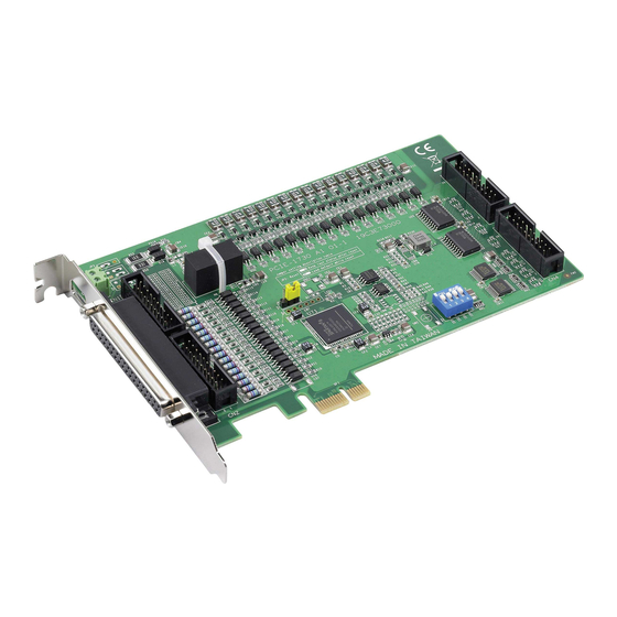
- Page 1 User Manual PCI-1730/1733/1734 32-ch Isolated Digital I/O PCI Cards...
- Page 2 No part of this manual may be reproduced, copied, translated or transmitted in any form or by any means without the prior written permission of Advantech Co., Ltd. Information provided in this manual is intended to be accurate and reliable. How- ever, Advantech Co., Ltd.
-
Page 3: Declaration Of Conformity
This product has passed the CE test for environmental specifications when shielded cables are used for external wiring. We recommend the use of shielded cables. This kind of cable is available from Advantech. Please contact your local supplier for ordering information. -
Page 4: Safety Instructions
If one of the following situations arises, get the equipment checked by service personnel: The power cord or plug is damaged. Liquid has penetrated into the equipment. The equipment has been exposed to moisture. PCI-1730/1733/1734 User Manual... - Page 5 The sound pressure level at the operator's position according to IEC 704-1:1982 is no more than 70 dB (A). Safety Precaution - Static Electricity DISCLAIMER: This set of instructions is given according to IEC 704-1. Advantech disclaims all responsibility for the accuracy of any statements contained herein.Safety Precaution - Static Electricity Follow these simple precautions to protect yourself from harm and the products from damage.
- Page 6 PCI-1730/1733/1734 User Manual...
-
Page 7: Table Of Contents
......9 Installation ....................10 Unpacking ....................10 Driver Installation ..................11 Figure 2.1 Advantech Automation Software Setup Screen ..11 Figure 2.2 Different Options for Driver Installation..... 12 Hardware Installation ................12 Figure 2.3 Device Manager ............13 Device Setup & Configuration ..............14 Figure 2.4 Device Manager Dialog Box ........ - Page 8 I/O Port Address Map ................38 Isolated Digital Input Registers ............... 40 Isolated Digital Output Register .............. 41 Non-isolated Digital Input Registers............41 Non-isolated Digital Output Register............42 Board ID — BASE+4H ................42 Interrupt Status Register ................. 43 PCI-1730/1733/1734 User Manual viii...
-
Page 9: Chapter 1 Overview
Chapter Overview... -
Page 10: Introduction
For easy monitoring, each isolated digital input channel is equipped with one red LED, and each isolated digital output channel is equipped with one green LED to show its ON/OFF status. The PCI-1730 and PCI-1733’s isolated digital input chan- nels are ideal for digital input in noisy environments or with floating potentials. - Page 11 Wide Input Range The PCI-1730/1733 has a wide range of input voltage from 5 to 30 VDC, and is suit- able for most industrial applications with 12 VDC or 24 VDC input voltage.
-
Page 12: Applications
Board ID The PCI-1730/1733/1734 has a built-in DIP Switch that helps define each card’s ID when multiple PCI-1730/1733/1734 cards have been installed on the same PC chas- sis. The board ID setting function is very useful when users build their system with multiple PCI-1730/1733/1734 cards. -
Page 13: Software Overview
Software Overview Advantech offers a rich set of DLL drivers, third-party driver support and application software to help fully exploit the functions of your PCI-1730/1733/1734 card: Device Drivers (on the companion CD-ROM) LabVIEW driver Advantech ActiveDAQ Advantech GeniDAQ Programming choices for DA&C cards: You may use Advantech application software such as Advantech Device Drivers. - Page 14 Function Overview chapter on the Device Drivers Manual. Programming with Device Drivers Function Library Advantech Device Drivers offers a rich function library to be utilized in various appli- cation programs. This function library consists of numerous APIs that support many development tools, such as Visual C++, Visual Basic, Delphi and C++ Builder.
-
Page 15: Accessories
Accessories Advantech offers a complete set of accessory products to support the PCI-1730/ 1733/1734 card. These accessories include: Wiring Cable The PCL-10137 shielded cable is specially designed for PCI-1730/1733/1734 cards to provide high resistance to noise. To achieve better signal quality, the signal wires are twisted in such a way as to form a “twisted-pair cable”, reducing cross-talk and... - Page 16 PCI-1730/1733/1734 User Manual...
-
Page 17: Chapter 2 Hardware Installation
Chapter Hardware Installation... -
Page 18: Installation
This chapter gives users a package item checklist, proper instructions about unpack- ing and step-by-step procedures for both driver and card installation. Unpacking After receiving your PCI-1730/1733/1734 package, please inspect its contents first. The package should contain the following items: PCI-1730/1733/1734 card Companion CD-ROM (Device Drivers included) User’s Manual... -
Page 19: Driver Installation
Driver Installation We recommend you to install the driver before you install the PCI-1730/1733/1734 card into your system, since this will guarantee a smooth installation process. The Advantech Device Driver Setup program for the PCI-1730/1733/ 1734 card is included on the companion CD-ROM that is shipped with your DA&C card package. -
Page 20: Figure 2.2 Different Options For Driver Installation
Touch the metal part on the surface of your computer to neutralize the static electricity that might be on your body. Insert the PCI-1730/1733/1734 card into a PCI slot. Hold the card only by its edges and carefully align it with the slot. Insert the card firmly into place. Use of excessive force must be avoided, otherwise the card might be damaged. -
Page 21: Figure 2.3 Device Manager
Device Manager: 1. Access the Device Manager through Control Panel/System/Device Manager. 2. The device name of the PCI-1730/1733/1734 should be listed on the Device Man- ager tab on the System Property Page. Figure 2.3 Device Manager... -
Page 22: Device Setup & Configuration
Select the device you want to configure from the list box and press the OK button. After you have clicked OK, you will see a PCI-1730 Device Setting dialog box such as the one in Fig. 2-6. -
Page 23: Figure 2.6 Device Setting Dialog Box
Configuring the Device On the PCI-1730 Device Setting dialog box (Fig. 2-6), you can configure the IDI00, IDI01 and DI00, DI01 Interrupt trigger mode either as Rising Edge or Fall- ing Edge, and Enable or Disable the IDI00, IDI01 and DI00, DI01. - Page 24 PCI-1730/1733/1734 User Manual...
-
Page 25: Chapter 3 Signal Connections
Chapter Signal Connections... -
Page 26: Overview
A good signal con- nection can avoid unnecessary and costly damage to your PC and other hardware devices. This chapter provides useful information about how to connect input and output signals to the PCI-1730/1733/1734 via the I/O connector. Switch and Jumper Settings PCI-1730 The PCI-1730 card has two function jumper settings. -
Page 27: Table 3.2: Board Id Setting (Sw1)
Table 3.2: Board ID setting (SW1) Board ID Note: On: 1, Off: 0 PCI-1733 Figure 3.2 Card Connector, Jumpers and Switches PCI-1730/1733/1734 User Manual... -
Page 28: Table 3.3: Board Id Setting (Sw1)
Table 3.3: Board ID setting (SW1) Board ID Note: On: 1, Off: 0 PCI-1734 The PCI-1734 card has one function jumper setting. Figure 3.3 Card Connector, Jumpers and Switches PCI-1730/1733/1734 User Manual... -
Page 29: Signal Connections
Table 3.4: Board ID setting (SW1) Board ID Note: On: 1, Off: 0 Signal Connections PCI-1730 (JP4, JP5: REV.A1) Pin Assignments IDO 0 1 IDO 1 IDI 0 IDI 1 IDO 2 3 IDO 3 IDI 2 IDI 3 IDO 4 5... - Page 30 IDO 13 Digital ground IDO 14 18 IDO 15 PCOM 19 Note: ECOM and PCOM are totally different. User must connect them carefully! PCI-1730 (JP4, JP5: REV.B2) Pin Assignments IDO 0 1 IDO 1 IDI 0 IDI 1 IDO 2 3...
- Page 31 IDO 9 Digital output IDO 10 16 IDO 11 GND: IDO 12 17 IDO 13 Digital ground IDO 14 18 IDO 15 PCOM 19 Note: ECOMn and PCOMn are totally different. User must be connect them carefully! PCI-1730/1733/1734 User Manual...
-
Page 32: Figure 3.4 Ttl-Level Di/O Connection
TTL-level Digital Input/Output The PCI-1730 has 16 TTL-level digital inputs and 16 TTL-level digital outputs. The following figure shows connections to exchange digital signals with other TTL devices: PCI-1730 TTL device Figure 3.4 TTL-level DI/O Connection If you want to receive an OPEN/SHORT signal from a switch or relay, add a pull-up resistor to ensure that the input is held at a high level when the contacts are open. -
Page 33: Figure 3.6 Isolated Di Connection
The following figure shows how to connect an external out- put load to the card's isolated outputs. Internal External Diode PCOM Common IDO0 IDO1 Isolated IDO2 Relay Circuit IDO3 IDO4 IDO5 IDO6 5~40V IDO7 EGND Figure 3.7 Isolated Digital Output Connection PCI-1730/1733/1734 User Manual... -
Page 34: Figure 3.8 Isolated Digital Input Connection
ECOM0. Channels 8 ~ 15 use ECOM1. Channels 16 ~ 23 use ECOM2. Channels 24 ~ 31 use ECOM3.) The following figure shows how to connect an external input source to the card's isolated inputs. External Internal IDI0 contact ECOM Isolated Circuit IDI1 Contact EGND Figure 3.8 Isolated Digital Input Connection PCI-1730/1733/1734 User Manual... - Page 35 IDO 15 9 PCOM IDO 16 10 IDO17 IDO 18 11 IDO19 IDO 20 12 IDO21 IDO 22 13 IDO23 PCOM 14 IDO24 IDO25 15 IDO26 IDO27 16 IDO28 IDO29 17 IDO30 IDO31 18 PCOM EGND 19 PCI-1730/1733/1734 User Manual...
-
Page 36: Figure 3.9 Isolated Digital Output Connection
The following figure shows how to connect an external output load to the card's isolated outputs. Internal External Diode PCOM Common IDO0 IDO1 Isolated IDO2 Relay Circuit IDO3 IDO4 IDO5 IDO6 5~40V IDO7 EGND Figure 3.9 Isolated Digital Output Connection PCI-1730/1733/1734 User Manual... -
Page 37: Appendix A Specifications
Appendix Specifications... -
Page 38: Specifications
+5 V @ 250 mA +12 V @ 35 mA Max. +5 V @ 400 mA Temperature Operation 0~+60°C (32~140°F) (refer to IEC 68-2-1,2) Storage -20~+85°C (-4~185°F) Relative Humidity 5~95%RH non-condensing (refer to IEC 68-2-3 ) Certification CE certified PCI-1730/1733/1734 User Manual... -
Page 39: Pci-1733
+5 V @ 200 mA +12 V @ 50 mA Max. +5 V @ 350 mA Temperature Operation 0~+60°C (32~140°F) (refer to IEC 68-2-1,2) Storage -20~+85°C (-4~185°F) Relative Humidity 5~95%RH non-condensing (refer to IEC 68-2-3 ) Certification CE certified PCI-1730/1733/1734 User Manual... -
Page 40: Pci-1734
+5 V @ 150 mA +12 V @ 15 mA Max. +5 V @ 250 mA Temperature Operation 0~+60°C (32~140°F) (refer to IEC 68-2-1,2) Storage -20~+85°C (-4~185°F) Relative Humidity 5~95%RH non-condensing (refer to IEC 68-2-3 ) Certification CE certified PCI-1730/1733/1734 User Manual... -
Page 41: Appendix B Block Diagram
Appendix Block Diagram... -
Page 42: Pci-1730
(IDI/O) EGND Control Control Bus Logic DI0 ~ DI7 PCI 9052 DI8 ~ DI15 DO0 ~ DO7 Box- Hander DO8 ~ DO15 20 Pin*2 (DI/O) Data Bus +12V Interrupt DI0 ~ DI1 Control IDI0 ~ IDI1 Logic PCI-1730/1733/1734 User Manual... -
Page 43: Pci-1733
Control Control Bus Logic Data Bus IDI0 ~ IDI7 PCI 9052 IDI8 ~ IDI15 Isolation D-Sub IDI16 ~IDI23 37 Pin Connector IDI24 ~ IDI31 ECOM0 ~ ECOM3 EGND Interrupt IDI0 ~ IDI1 Control IDI16 ~ IDI17 Logic PCI-1730/1733/1734 User Manual... -
Page 44: Pci-1734
PCI-1734 Address Bus Control Control Bus Logic Data Bus IDO0 ~ IDO7 PCI 9052 IDO8 ~ IDO15 Isolation D-Sub IDO16 ~IDO23 37 Pin Connector IDO24 ~ IDO31 PCOM0 ~ PCOM3 EGND PCI-1730/1733/1734 User Manual... -
Page 45: Appendix C Register Structure & Format
Appendix Register Structure & Format... -
Page 46: Overview
For example, BASE+0 is the card's base address and BASE+6 is the base address plus six bytes. The table C-1 shows the function of each register of the PCI-1730/ 1733/1734 or driver and its address relative to the card's base address. - Page 47 IDI16EN IDI1EN IDI0EN Interrupt Enable Register IDI17EN IDI16EN IDI1EN IDI0EN Interrupt Triggering Status IDI17RF IDI16RF IDI1RF IDI0RF Interrupt Triggering Register IDI17RF IDI16RF IDI1RF IDI0RF Interrupt Flag IDI17F IDI16F IDI1F IDI0F Interrupt Clear Register IDI17CLR IDI16CLR IDI1CLR IDI0CLR PCI-1730/1733/1734 User Manual...
-
Page 48: Isolated Digital Input Registers
IDO25 IDO24 Board ID Register Isolated Digital Input Registers BASE+0H/1H (/2H/3H) The PCI-1730 offers 16-ch isolated digital input channels. These channels use the input ports at addresses BASE+0H/1H. Table C-1 Register for Isolated Digital Input Read Isolated Digital Input Bit #... -
Page 49: Isolated Digital Output Register
IDO28 IDO27 IDO26 IDO25 IDO24 Non-isolated Digital Input Registers BASE+2H/3H The PCI-1730 offers 16-ch digital input channels. These channels use the input ports at addresses BASE+2H/3H. Table C-5 Register for Digital Input Read Digital Input Bit # BASE + 2H... -
Page 50: Non-Isolated Digital Output Register
Non-isolated Digital Output Register BASE+2H/3H The PCI-1730 offers 16-ch digital output channels. These channels use the input ports at addresses BASE+2H/3H. Table C-6 Register for Digital Output Write Digital Output Bit # BASE + 2H BASE + 3H DO15 DO14... -
Page 51: Interrupt Status Register
Interrupt Status Register BASE+8H/CH/10H The PCI-1730 Interrupt Status Register control the status of four interrupt signal sources (IDI0, IDI1, DI0, DI1). Table C-8 Register for Interrupt Status Read Interrupt Status Register Bit # BASE + 8H DI1EN DI0EN IDI1EN IDI0EN... - Page 52 Falling edge trigger C.9 Interrupt Control Register — BASE+8H/CH/10H The PCI-1730 Interrupt Control Register controls the status of four interrupt signal sources (IDI0, IDI1, DI0, DI1). The user can clear the interrupt by writing its corre- sponding value to the Interrupt Control Register, as shown in below table.
- Page 53 Interrupt triggering control bits (n = 0, 1, 16, 17) The interrupt can be triggered by a rising edge or falling edge of the interrupt signal, as determined by the value in this bit. Rising edge trigger Falling edge trigger PCI-1730/1733/1734 User Manual...
- Page 54 No part of this publication may be reproduced in any form or by any means, electronic, photocopying, recording or otherwise, without prior written permis- sion of the publisher. All brand and product names are trademarks or registered trademarks of their respective companies. © Advantech Co., Ltd. 2007...
Need help?
Do you have a question about the PCI-1730 and is the answer not in the manual?
Questions and answers