Table of Contents
Advertisement
Quick Links
This documentation and the software included with this product are
copyrighted 1999 by Advantech Co., Ltd. All rights are reserved.
Advantech Co., Ltd. reserves the right to make improvements in the
products described in this manual at any time without notice.
No part of this manual may be reproduced, copied, translated or
transmitted in any form or by any means without the prior written
permission of Advantech Co., Ltd. Information provided in this
manual is intended to be accurate and reliable. However, Advantech
Co., Ltd. assumes no responsibility for its use, nor for any infringe-
ments of the rights of third parties which may result from its use.
PC-LabCard is a trademark of Advantech Co., Ltd. IBM and PC are
trademarks of International Business Machines Corporation. MS-
DOS, Windows, Microsoft Visual C++ and Visual BASIC are trade-
marks of Microsoft Corporation. Intel and Pentium are trademarks of
Intel Corporation. Delphi and C++Builder are trademarks of Inprise
Corporation.
The PCI-1711/1731, developed by ADVANTECH CO., LTD., has
passed the CE test for environmental specifications when shielded
cables are used for external wiring. We recommend the use of
shielded cables. This kind of cable is available from Advantech.
Please contact your local supplier for ordering information.
For technical support and service, please visit our support website at:
http://support.advantech.com
Part No. 2003171100
Printed in Taiwan
1st Edition
October 1999
Advertisement
Table of Contents

Related Manuals for Advantech PCI-1711


Summary of Contents for Advantech PCI-1711
- Page 1 Co., Ltd. assumes no responsibility for its use, nor for any infringe- ments of the rights of third parties which may result from its use. PC-LabCard is a trademark of Advantech Co., Ltd. IBM and PC are trademarks of International Business Machines Corporation. MS- DOS, Windows, Microsoft Visual C++ and Visual BASIC are trade- marks of Microsoft Corporation.
-
Page 2: Table Of Contents
Contents 1. Introduction ..........1 1.1 Features ................1 1.2 Installation Guide ..............3 1.3 Software ................5 1.4 Accessories ................5 2. Installation ............. 7 2.1 Unpacking ................7 2.2 Driver Installation ..............8 2.3 Hardware Installation ............9 2.4 Device Setup &... -
Page 3: Appendix B Block Diagram
Appendix B Block Diagram ..........35 Appendix C Register Structure and Format ....37 C.1 Overview ................37 C.2 I/O Port Address Map ............37 C.3 Channel Number and A/D Data — BASE+0 and BASE+1 ................42 C.4 Software A/D Trigger — BASE+0 ........42 C.5 A/D Channel Range Setting —... -
Page 5: Introduction
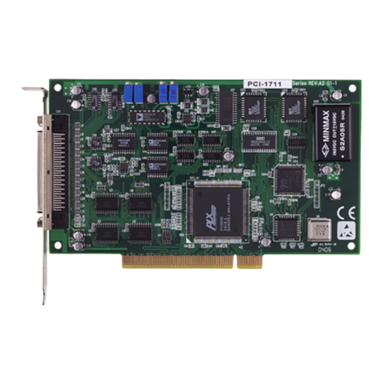
Chapter 1 Chapter 1. Introduction Thank you for buying the Advantech PCI-1711/1731 PCI card. The Advantech PCI-1711/1731 is a powerful data acquisition (DAS) card for the PCI bus. It features a unique circuit design and complete functions for data acquisition and control. PCI-1711/1731 provides specific... - Page 6 Optional D/A Output for Cost Savings The PCI-1711 goes further with 2 analog output channels, while the PCI-1731 doesn’t. It is for users to differentiate between the PCI-1711 and the PCI-1731 according to what they really need as the best solution with no extra cost.
-
Page 7: Installation Guide
Chapter 1 1.2 Installation Guide Before you install your PCI-1711/1731 card, please make sure you have the following necessary components: PCI-1711 or PCI-1731 DAS card PCI-1711/1731 User’s Manual Driver software Advantech DLL drivers (included in the companion CD-ROM) Wiring cable... - Page 8 U se testing utility to test ha rdw are R e ad e xa m ples & driver m anu al S tart to w rite your a pplication Fig. 1-1 Installation Flow Chart Advantech Co., Ltd. PCI-1711/1731 User’s Manual – 4 – www.advantech.com...
-
Page 9: Software
Chapter 1 1.3 Software Advantech offers a rich set of DLL drivers, third-party driver support and application software to help fully exploit the functions of your PCI-1711/1731 card: DLL driver (on the companion CD-ROM) Labview driver Advantech ActiveDAQ Advantech GeniDAQ For more information on software, please refer to Chapter 4, Software Overview. - Page 10 Reserved space on the board to meet future needs for signal- conditioning circuits (low-pass filter, voltage attenuator and current shunt) Industrial-grade screw-clamp terminal blocks for heavy-duty and reliable connections. Advantech Co., Ltd. PCI-1711/1731 User’s Manual – 6 – www.advantech.com...
-
Page 11: Installation
This chapter gives users a package item checklist, proper instructions about unpacking and step-by-step procedures for both driver and card installation. 2.1 Unpacking After receiving your PCI-1711/1731 package, please inspect its contents first. The package should contain the following items: PCI-1711/1731 card Companion CD-ROM (DLL driver included) User’s Manual... -
Page 12: Driver Installation
1711/1731 card into your system, since this will guarantee a smooth installation process. The 32-bit DLL driver Setup program for the PCI-1711/1731 card is included on the companion CD-ROM that is shipped with your DAS card package. Please follow the steps below to install the driver software: Step 1: Insert the companion CD-ROM into your CD-ROM drive. -
Page 13: Hardware Installation
(please refer to 2.2 Driver Installation) After the DLL driver installation is completed, you can now go on to install the PCI-1711/1731 card in any PCI slot on your computer. But it is suggested that you should refer to the computer user manual or related documentations if you have any doubt. - Page 14 Step 4: Touch the metal part on the surface of your computer to neutralize the static electricity that might be on your body. Step 5: Insert the PCI-1711/1731 card into a PCI slot. Hold the card only by its edges and carefully align it with the slot. Insert the card firmly into place.
- Page 15 Device Manager by selecting its device name and press the Remove button. Then go through the driver installation process again. Fig. 2-4 The “exclamation mark” (!) on the device name indicating improper installation of the card Advantech Co., Ltd. – 11 – PCI-1711/1731 User’s Manual www.advantech.com...
-
Page 16: Device Setup & Configuration
Step 1: To install the I/O device for your card, you must first run the Device Installation program (by accessing Start/Programs/ Advantech Driver for 95 and 98 (or for NT)/Device Installa- tion). Fig. 2-5 The Advantech Device Installation utility program Step 2: On the Device Installation program window, select the Setup menu item on the menu bar, and click the Device command (Fig. - Page 17 Select the device you want to configure from the list box and press the OK button. After you have clicked OK, you will see a Device Setting dialog box such as the one in Fig. 2-9. Advantech Co., Ltd. – 13 – PCI-1711/1731 User’s Manual www.advantech.com...
- Page 18 : By inputting an external reference voltage: -xV , where |x| <= 10, you will get a output voltage range: 0 to xV. Advantech Co., Ltd. PCI-1711/1731 User’s Manual – 14 – www.advantech.com...
-
Page 19: Device Testing
Fig. 2-10 The Device Name appearing on the list of devices box Note: As we have noted, the device name “000:PCI-1711 I/O=6500H” begins with a device number “000”, which is specifically assigned to each card cifically. The device number is passed to the driver to specify which device you wish to control. - Page 20 Chapter 2 On the Device Test dialog box, users are free to test various functions of PCI-1711/1731 on the Analog input, Analog output, Digital input, Digital output or Counter tabs. Note: You can access the Device Test dialog box either by the previous...
- Page 21 By pressing the buttons on each tab, users can easily set each digital output channel as high or low for the corresponding port. Advantech Co., Ltd. – 17 – PCI-1711/1731 User’s Manual www.advantech.com...
- Page 22 Only after your card device is properly set up, configured and tested, can the device installation procedure be counted as complete. After the device installation procedure is completed, you can now safely proceed to the next chpater, Signal Connections. Advantech Co., Ltd. PCI-1711/1731 User’s Manual – 18 – www.advantech.com...
-
Page 23: Signal Connections
PCI-1711/1731 via the I/O connector. 3.2 I/O Connector The I/O connector on the PCI-1711/1731 is a 68-pin connector that enable you to connect to accessories with the PCL-10168 shielded cable. - Page 24 C N T 0 _ G AT E + 1 2 V + 5 V Fig. 3-1 I/O connector pin assignments for the PCI-1711/1731 *: Pins 23~ 25 and pins 57 ~ 59 are not defined for PCI-1731 Advantech Co., Ltd.
- Page 25 A/D conversion. A low-to-high edge triggers A/D conversion to start. +12V DGND Output +12 VDC Source. DGND Output +5 VDC Source. Table 3-1 I/O Connector Signal Description Advantech Co., Ltd. – 21 – PCI-1711/1731 User’s Manual www.advantech.com...
-
Page 26: Analog Input Connections
A signal source without a local ground is also called a “floating source”. It is fairly simple to connect a single-ended channel to a floating signal source. In this mode, the PCI-1711/1731 provides a reference ground for external floating signal sources. -
Page 27: Trigger Source Connections
32-bit timer for pacer triggering. A low-to-high edge from the Counter 2 output (PACER_OUT) will trigger an A/D conversion on the PCI-1711/1731. At the same time, you can also use this signal as a synchronous signal for other applications. -
Page 28: Field Wiring Considerations
3.6 Field Wiring Considerations When you use the PCI-1711/1731 to acquire data from outside, noises in the environment might significantly affect the accuracy of your measurements if due cautions are not taken. The following measures will be helpful to reduce possible interference running signal wires between signal sources and the PCI-1711/1731. -
Page 29: Software Overview
DLL Driver The Advantech DLL Drivers software is included on the companion CD-ROM at no extra charge. It also comes with all the Advantech DAS cards. Advantech’s DLL driver features a complete I/O function library to help boost your application performance. The Advantech DLL Advantech Co., Ltd. - Page 30 Since register-level programming requires much effort and time, we recommend that you use the Advantech DLL drivers instead. However, if register-level programming is indispensible, you should refer to the relevant information in Appendix C, Register Structure and Format, or to the example codes included on the companion CD-ROM.
-
Page 31: Dll Driver Programming Roadmap
C++ Builder For instructions on how to begin programming works in each develop- ment tool, Advantech offers a Tutorial Chapter in the DLL Drivers Manual for your reference. Please refer to the corresponding sections in this chapter on the DLL Drivers Manual to begin your programming efforts. - Page 32 Or you can refer to the DLL Driver Error Codes Appendix in the DLL Drivers Manaul for a detailed listing of the Error Code, Error ID and the Error Message. Advantech Co., Ltd. PCI-1711/1731 User’s Manual – 28 – www.advantech.com...
-
Page 33: Calibration
D. C. voltage source. 5.1 VR Assignment There are four variable resistors (VRs) on the PCI-1711 card and two variable resistors (VRs) on the PCI-1731 card. These variable resistors are to facilitate accurate adjustments for all A/D and D/A channels. -
Page 34: A/D Calibration
You can select the on-board -5V or -10V internal reference voltage or an external voltage as your analog output reference voltage. If you use an external reference, connect a reference voltage within the range Advantech Co., Ltd. PCI-1711/1731 User’s Manual – 30 – www.advantech.com... -
Page 35: Self A/D Calibration
AI0 focused on FFE (at least 70%) and adjust VR1 until the output codes from the card’s AI1, AI2, AI3, AI4 and AI5 focused on 7FF (at least 70%). 6. Press the SPACE key to finish calibration procedures. Advantech Co., Ltd. – 31 – PCI-1711/1731 User’s Manual www.advantech.com... - Page 36 Chapter 5 Advantech Co., Ltd. PCI-1711/1731 User’s Manual – 32 – www.advantech.com...
-
Page 37: Appendix A Specifications
INL: ± 0.5 LSB Monotonicity: 12 bits Accuracy Offset error: Adjustable to zero SNR: 68 dB ENOB: 11 bits Analog Output Only for PCI-1711 s l e i t u t i b Internal Reference 0 ~ +5 V, 0 ~ +10 V Output Range (Internal &... - Page 38 +5 V @ 700 mA Power Consumption Max. +5 V @ 1.0 A 0~+60°C(32~140°F) Operation (refer to IEC 68-2-1,2) Temperature Storage -20~+70°C(-4~158°F) 5~95%RH non-condensing Relative Humidity (refer to IEC 68-2-3) Advantech Co., Ltd. PCI-1711/1731 User’s Manual – 34 – www.advantech.com...
-
Page 39: Block Diagram
C h a n n e l S ca n L o g ic 1 6 S /E G a in C o n tro l R A M AI15 Advantech Co., Ltd. – 35 – PCI-1711/1731 User’s Manual www.advantech.com... - Page 40 APPENDIX B Advantech Co., Ltd. PCI-1711/1731 User’s Manual – 36 – www.advantech.com...
-
Page 41: Register Structure And Format
The PCI-1711/1731 is delivered with an easy-to-use 32-bit DLL driver for user programming under the Windows 95/98/NT operating system. We advise users to program the PCI-1711/1731 using the 32- bit DLL driver provided by Advantech to avoid the complexity of low-level programming by register. - Page 42 APPENDIX C Table C-1 PCI-1711/1731 register format (Part 1) Base Read Address + decimal Channel Number and A/D Data AD11 AD10 Status Register CNT0 ONE/FH IRQEN GATE PACER Advantech Co., Ltd. PCI-1711/1731 User’s Manual – 38 – www.advantech.com...
- Page 43 APPENDIX C Table C-1 PCI-1711/1731 register format (Part 2) Base Read Address + decimal Digital Input DI15 DI14 DI13 DI12 DI11 DI10 Counter 0 Counter 1 Counter 2 Advantech Co., Ltd. – 39 – PCI-1711/1731 User’s Manual www.advantech.com...
- Page 44 APPENDIX C Table C-1 PCI-1711/1731 register format (Part 3) Base Write Address + decimal Software A/D Trigger A/D Channel Range Setting MUX Control Stop channel Start channel Control Register CNT0 ONE/FH IRQEN GATE PACER Clear Interrupt and FIFO clear FIFO...
- Page 45 APPENDIX C Table C-1 PCI-1711/1731 register format (Part 4) Base Write Address + decimal D/A Reference Control DA1_I/E DA1_5/10 DA0_I/E DA0_5/10 Digital Output DO15 DO14 DO13 DO12 DO11 DO10 Counter 0 Counter 1 Counter 2 Counter Control Advantech Co., Ltd.
-
Page 46: Channel Number And A/D Data - Base+0 And Base+1
BASE+6, Bit 2 to bit 0, select the trigger source. (see Section C.7, Control Register -- BASE+6 ) If you select software triggering, a write to the register BASE+0 with any value will trigger an A/D conversion. Advantech Co., Ltd. PCI-1711/1731 User’s Manual – 42 – www.advantech.com... -
Page 47: A/D Channel Range Setting - Base+2
Write A/D channel range setting Bit # BASE+2 where G2 to G0 are Gain Codes and table C-4 lists the gain codes for the PCI-1711/1731. Table C-4 Gain codes for PCI-1711/1731 PCI-1711/1731 Gain Code Gain Input Range(V) -10 to +10 -5 to +5 -2.5 to +2.5... -
Page 48: Mux Control - Base+4 And Base+5
If the start scan input channel is AI3 and the stop scan input channel is AI7, then the scan sequence is AI3, AI4, AI5, AI6, AI7, AI3, AI4, AI5, AI6, AI7, AI3, AI4… Advantech Co., Ltd. PCI-1711/1731 User’s Manual – 44 – www.advantech.com... -
Page 49: Status Register - Base+6 And Base+7
This bit indicates whether the FIFO is full. 1 means that the FIFO is full. Interrupt flag This bit indicates the interrupt status. 1 means that an interrupt has occurred. Advantech Co., Ltd. – 45 – PCI-1711/1731 User’s Manual www.advantech.com... -
Page 50: Control Register - Base+6
0 the clock source of Counter 0 comes from the internal clock (1 MHz) 1 the clock source of Counter 0 comes from the external clock (maximum up to 10 MHz). Advantech Co., Ltd. PCI-1711/1731 User’s Manual – 46 – www.advantech.com... -
Page 51: Clear Interrupt And Fifo - Base+8 And Base+9
Table C-9 Register for D/A channel 0 data Write D/A Output Channel 0 Bit # BASE+11 DA11 DA10 BASE+10 DA11 ~ DA0 Digital to analog data LSB of the D/A data DA11 MSB of the D/A data Advantech Co., Ltd. – 47 – PCI-1711/1731 User’s Manual www.advantech.com... -
Page 52: D/A Output Channel 1 - Base+12 And Base+13
D/A Output Channel 1 Bit # BASE+13 DA11 DA10 BASE+12 DA11 ~ DA0 Digital to analog data the LSB of the D/A data DA11 the MSB of the D/A data Advantech Co., Ltd. PCI-1711/1731 User’s Manual – 48 – www.advantech.com... -
Page 53: D/A Reference Control -Base+14
The internal reference voltage for D/A output channel 1 - 5 V - 10 V DA1_I/E Internal or external reference voltage for D/A output channel 1 internal source external source Advantech Co., Ltd. – 49 – PCI-1711/1731 User’s Manual www.advantech.com... -
Page 54: Digital I/O Registers - Base+16 And Base+17
APPENDIX C C.13 Digital I/O Registers — BASE+16 and BASE+17 The PCI-1711/1731 offers 16 digital input channels and 16 digital output channels. These I/O channels use the input and output ports at addresses BASE+16 and BASE+17. Table C-12 Register for digital input... -
Page 55: Appendix D 82C54 Counter Function
Counter 0 On the PCI-1711/1731, counter 0 can be a 16-bit timer or an event counter, selectable by users. When the clock source is set as an internal source, counter 0 is a 16-bit timer; when set as an external source, then counter 0 is an event counter and the clock source comes from CNT0_CLK. - Page 56 Programmable one shot Rate generator Square wave rate generator Software triggered strobe Hardware triggered strobe BCD Select binary or BCD counting Type Binary counting 16-bits Binary coded decimal (BCD) counting Advantech Co., Ltd. PCI-1711/1731 User’s Manual – 52 – www.advantech.com...
-
Page 57: Counter Operating Modes
The counter continues to decrement after it reaches the terminal count. Rewriting a counter register during counting has the following results: 1.Writing to the first byte stops the current counting. Advantech Co., Ltd. – 53 – PCI-1711/1731 User’s Manual www.advantech.com... - Page 58 In this way, if the count is odd, the output will be high for (N+1)/2 counts and low for (N-1)/2 counts. Advantech Co., Ltd. PCI-1711/1731 User’s Manual – 54 – www.advantech.com...
-
Page 59: Counter Operations
The read-back command can latch multiple counter output latches. Simply set the CNT bit to 0 and select the desired counter(s). This single command is functionally equivalent to multiple counter latch commands, one for each counter latched. Advantech Co., Ltd. – 55 – PCI-1711/1731 User’s Manual www.advantech.com... - Page 60 1 and CNT = 0. The second method has the advantage of operating several counters at the same time. A subsequent read operation on the selected counter will retrieve the latched value. Advantech Co., Ltd. PCI-1711/1731 User’s Manual – 56 – www.advantech.com...
Need help?
Do you have a question about the PCI-1711 and is the answer not in the manual?
Questions and answers