Table of Contents
Advertisement
Quick Links
Download this manual
See also:
User Manual
Advertisement
Table of Contents

Related Manuals for Advantech PCI-1730U


Summary of Contents for Advantech PCI-1730U
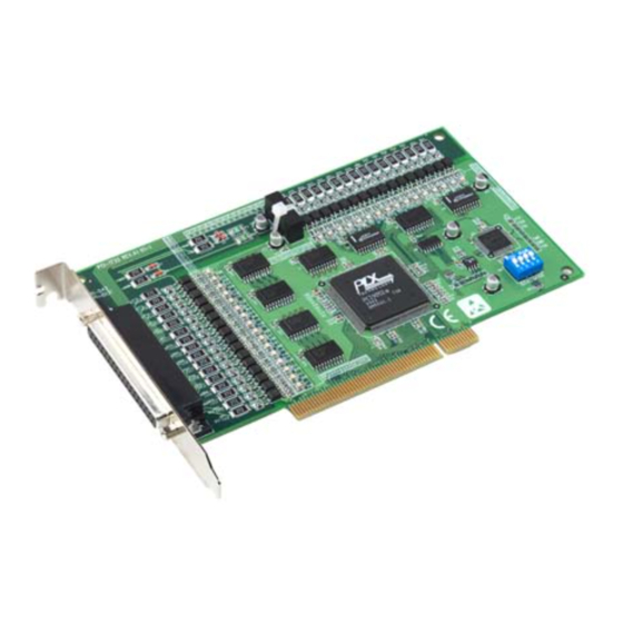
- Page 1 User Manual PCI-1730U/1733/1734 32-ch Isolated Digital I/O PCI Cards...
- Page 2 No part of this manual may be reproduced, copied, translated or transmitted in any form or by any means without the prior written permission of Advantech Co., Ltd. Information provided in this manual is intended to be accurate and reliable. How- ever, Advantech Co., Ltd.
-
Page 3: Declaration Of Conformity
This product has passed the CE test for environmental specifications when shielded cables are used for external wiring. We recommend the use of shielded cables. This kind of cable is available from Advantech. Please contact your local supplier for ordering information. -
Page 4: Safety Instructions
Liquid has penetrated into the equipment. The equipment has been exposed to moisture. The equipment does not work well, or you cannot get it to work according to the user's manual. The equipment has been dropped and damaged. PCI-1730U/1733/1734 User Manual... - Page 5 70 dB (A). Safety Precaution - Static Electricity DISCLAIMER: This set of instructions is given according to IEC 704-1. Advantech disclaims all responsibility for the accuracy of any statements contained herein. Follow these simple precautions to protect yourself from harm and the products from damage.
- Page 6 PCI-1730U/1733/1734 User Manual...
-
Page 7: Table Of Contents
Figure 3.3 Card Connector, Jumpers and Switches ....14 Table 3.4: Board ID setting (SW1)..........15 Signal Connections ................. 15 3.3.1 PCI-1730U Pin Assignments ............15 Figure 3.4 TTL-level DI/O Connection ........16 Figure 3.5 Open/Short Connection ..........17 Figure 3.6 Isolated DI Connection ..........17 Figure 3.7 Isolated Digital Output Connection ...... - Page 8 I/O Port Address Map ................30 Isolated Digital Input Registers ............... 32 Isolated Digital Output Register .............. 33 Non-isolated Digital Input Registers............33 Non-isolated Digital Output Register............34 Board ID — BASE+4H ................34 Interrupt Status Register ................. 35 PCI-1730U/1733/1734 User Manual viii...
-
Page 9: Chapter 1 Overview
Chapter Overview... -
Page 10: Introduction
For easy monitoring, each isolated digital input channel is equipped with one red LED, and each isolated digital output channel is equipped with one green LED to show its ON/OFF status. The PCI-1730U and PCI-1733’s isolated digital input chan- nels are ideal for digital input in noisy environments or with floating potentials. - Page 11 Wide Input Range The PCI-1730U/1733 has a wide range of input voltage from 5 to 30 VDC, and is suit- able for most industrial applications with 12 VDC or 24 VDC input voltage.
-
Page 12: Applications
Board ID The PCI-1730U/1733/1734 has a built-in DIP Switch that helps define each card’s ID when multiple PCI-1730U/1733/1734 cards have been installed on the same PC chassis. The board ID setting function is very useful when users build their system with multiple PCI-1730U/1733/1734 cards. -
Page 13: Software Overview
Software Overview Advantech offers a rich set of DLL drivers, third-party driver support and application software to help fully exploit the functions of your PCI-1730U/1733/1734 card: – Device Drivers (on the companion DVD-ROM) – LabVIEW driver – Advantech DAQ NAVi –... - Page 14 PCI-1730U/1733/1734 User Manual...
-
Page 15: Chapter 2 Installation
Chapter Installation... -
Page 16: Unpacking
Unpacking After receiving your PCI-1730U/1733/1734 package, please inspect its contents first. The package should contain the following items: PCI-1730U/1733/1734 card Companion CD-ROM (Device Drivers included) Startup Manual The PCI-1730U/1733/1734 card harbors certain electronic components vulnerable to electrostatic discharge (ESD). ESD could easily damage the integrated circuits and certain components if preventive measures are not carefully paid attention to. -
Page 17: Hardware Installation
Touch the metal part on the surface of your computer to neutralize the static electricity that might be on your body. Insert the PCI-1730U/1733/1734 card into a PCI slot. Hold the card only by its edges and carefully align it with the slot. Insert the card firmly into place. Use of excessive force must be avoided, otherwise the card might be damaged. - Page 18 PCI-1730U/1733/1734 User Manual...
-
Page 19: Chapter 3 Signal Connections
Chapter Signal Connections... -
Page 20: Overview
A good signal con- nection can avoid unnecessary and costly damage to your PC and other hardware devices. This chapter provides useful information about how to connect input and output signals to the PCI-1730U/1733/1734 via the I/O connector. Switch and Jumper Settings 3.2.1 PCI-1730U The PCI-1730U card has two function jumper settings. -
Page 21: Pci-1733
Table 3.2: Board ID setting (SW1) Board ID Note: On: 1, Off: 0 3.2.2 PCI-1733 Figure 3.2 Card Connector, Jumpers and Switches PCI-1730U/1733/1734 User Manual... -
Page 22: Pci-1734
Table 3.3: Board ID setting (SW1) Board ID Note: On: 1, Off: 0 3.2.3 PCI-1734 The PCI-1734 card has one function jumper setting. Figure 3.3 Card Connector, Jumpers and Switches PCI-1730U/1733/1734 User Manual... -
Page 23: Signal Connections
Table 3.4: Board ID setting (SW1) Board ID Note: On: 1, Off: 0 Signal Connections 3.3.1 PCI-1730U Pin Assignments IDO 0 IDO 1 IDI 0 IDI 1 IDO 2 IDO 3 IDI 2 IDI 3 IDO 4 IDO 5 IDI 4... -
Page 24: Figure 3.4 Ttl-Level Di/O Connection
DOn (n=0 ~ 15): Digital output GND: Digital ground TTL-level Digital Input/Output The PCI-1730U has 16 TTL-level digital inputs and 16 TTL-level digital outputs. The following figure shows connections to exchange digital signals with other TTL devices: PCI-1730 TTL device Figure 3.4 TTL-level DI/O Connection... -
Page 25: Figure 3.5 Open/Short Connection
Channels 8 ~ 15 use ECOM1.) The following figure shows how to connect an exter- nal input source to the card's isolated inputs. External Internal IDI0 contact ECOM Isolated Circuit IDI1 Contact EGND Figure 3.6 Isolated DI Connection PCI-1730U/1733/1734 User Manual... -
Page 26: Pci-1733 Pin Assignments
Figure 3.7 Isolated Digital Output Connection 3.3.2 PCI-1733 Pin Assignments Description of pin use: IDIn (n=0 ~ 31): Isolated digital input ECOM n (n=0 ~ 3): External common Vcc/GND of IDI EGND: External ground for IDI PCI-1730U/1733/1734 User Manual... -
Page 27: Pci-1734 Pin Assignments
EGND Figure 3.8 Isolated Digital Input Connection 3.3.3 PCI-1734 Pin Assignments Description of pin use: IDOn (n=0 ~ 31): Isolated digital output PCOM n (n=0 ~ 3): Free wheeling common diode for EGND: External ground for IDO PCI-1730U/1733/1734 User Manual... -
Page 28: Figure 3.9 Isolated Digital Output Connection
A. If the current for all channels combined exceeds 2 A, CN2 must be connected to the external ground to share the extra current. The following figure shows how to connect an external output load to the card's isolated outputs. Figure 3.9 Isolated Digital Output Connection PCI-1730U/1733/1734 User Manual... -
Page 29: Appendix A Specifications
Appendix Specifications... -
Page 30: Specifications
+5 V @ 250 mA +12 V @ 35 mA Max. +5 V @ 400 mA Temperature Operation 0~+60°C (32~140°F) (refer to IEC 68-2-1,2) Storage -20~+85°C (-4~185°F) Relative Humidity 5~95%RH non-condensing (refer to IEC 68-2-3) Certification CE/FCC PCI-1730U/1733/1734 User Manual... -
Page 31: Pci-1733
+12V @ 15 mA (typical) +5V @ 250 mA (max.) Temperature Operating: 0 ~ +60°C (32 ~ 140°F) Storage: -20 ~ +70°C (-4 ~ 158°F) Relative Humidity 5 – 95 % RH non-condensing (refer to IEC 60068-2-3) Certifications CE / FCC PCI-1730U/1733/1734 User Manual... - Page 32 PCI-1730U/1733/1734 User Manual...
-
Page 33: Appendix B Block Diagram
Appendix Block Diagram... -
Page 34: Pci-1730U Block Diagram
PCI-1730U Block Diagram PCI-1733 Block Diagram PCI-1730U/1733/1734 User Manual... -
Page 35: Pci-1734 Block Diagram
PCI-1734 Block Diagram PCI-1730U/1733/1734 User Manual... - Page 36 PCI-1730U/1733/1734 User Manual...
-
Page 37: Appendix C Register Structure & Format
Appendix Register Structure & Format... -
Page 38: Overview
For example, BASE+0 is the card's base address and BASE+6 is the base address plus six bytes. The table C-1 shows the function of each register of the PCI-1730U/ 1733/1734 or driver and its address relative to the card's base address. - Page 39 IDI16EN IDI1EN IDI0EN Interrupt Enable Register IDI17EN IDI16EN IDI1EN IDI0EN Interrupt Triggering Status IDI17RF IDI16RF IDI1RF IDI0RF Interrupt Triggering Register IDI17RF IDI16RF IDI1RF IDI0RF Interrupt Flag IDI17F IDI16F IDI1F IDI0F Interrupt Clear Register IDI17CLR IDI16CLR IDI1CLR IDI0CLR PCI-1730U/1733/1734 User Manual...
-
Page 40: Isolated Digital Input Registers
IDO25 IDO24 Board ID Register Isolated Digital Input Registers BASE+0H/1H (/2H/3H) The PCI-1730U offers 16-ch isolated digital input channels. These channels use the input ports at addresses BASE+0H/1H. Table C-1 Register for Isolated Digital Input Read Isolated Digital Input Bit #... -
Page 41: Isolated Digital Output Register
Isolated Digital Output Register BASE+0H/1H (/2H/3H) The PCI-1730U offers 16-ch isolated digital output channels. These channels use the registries at addresses BASE+0H/1H. Table C-3 Register for Isolated Digital Output Write Isolated Digital Output Bit # BASE + 0H IDO7 IDO6... -
Page 42: Non-Isolated Digital Output Register
Non-isolated Digital Output Register BASE+2H/3H The PCI-1730U offers 16-ch digital output channels. These channels use the input ports at addresses BASE+2H/3H. Table C-6 Register for Digital Output Write Digital Output Bit # BASE + 2H BASE + 3H DO15 DO14... -
Page 43: Interrupt Status Register
Interrupt Status Register BASE+8H/CH/10H The PCI-1730U Interrupt Status Register control the status of four interrupt signal sources (IDI0, IDI1, DI0, DI1). Table C-8 Register for Interrupt Status Read Interrupt Status Register Bit # BASE + 8H DI1EN DI0EN IDI1EN IDI0EN... - Page 44 Falling edge trigger C.9 Interrupt Control Register — BASE+8H/CH/10H The PCI-1730U Interrupt Control Register controls the status of four interrupt sig- nal sources (IDI0, IDI1, DI0, DI1). The user can clear the interrupt by writing its corre- sponding value to the Interrupt Control Register, as shown in below table.
- Page 45 Interrupt triggering control bits (n = 0, 1, 16, 17) The interrupt can be triggered by a rising edge or falling edge of the interrupt signal, as determined by the value in this bit. Rising edge trigger Falling edge trigger PCI-1730U/1733/1734 User Manual...
- Page 46 No part of this publication may be reproduced in any form or by any means, electronic, photocopying, recording or otherwise, without prior written permis- sion of the publisher. All brand and product names are trademarks or registered trademarks of their respective companies. © Advantech Co., Ltd. 2011...
Need help?
Do you have a question about the PCI-1730U and is the answer not in the manual?
Questions and answers