Table of Contents
Advertisement
Quick Links
Advertisement
Table of Contents

Related Manuals for Advantech PCI-1724U


Summary of Contents for Advantech PCI-1724U
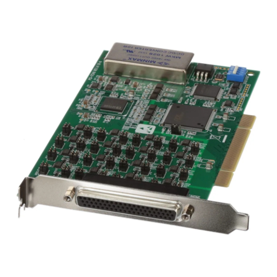
- Page 1 PCI-1724U 14-bit, 32-ch, Isolated Analog Output Card User Manual...
- Page 2 No part of this man- ual may be reproduced, copied, translated or transmitted in any form or by any means without the prior written permission of Advantech Co., Ltd. Information provided in this manual is intended to be accurate and reli- able.
- Page 3 Product Warranty (2 years) Advantech warrants to you, the original purchaser, that each of its prod- ucts will be free from defects in materials and workmanship for two years from the date of purchase. This warranty does not apply to any products which have been repaired or...
- Page 4 Before setting up the system, check that the items listed below are included and in good condition. If any item does not accord with the table, please contact your dealer immediately. Before you install your PCI-1724U card, please make sure you have the following necessary components: • 1 x PCI-1724U card •...
-
Page 5: Table Of Contents
3.2.4 Board ID setting ............24 Signal Connections ............25 3.3.1 Pin Assignment ............25 Figure 3.2:I/O Conn. Pin Assg. for the PCI-1724U ..25 3.3.2 I/O Connector Signal Descriptions ......26 Table 3.1:I/O Connector Signal Descriptions ....26 3.3.3 Analog Output Connection .......... - Page 6 Overview ................. 34 Table C.1:PCI-1724U Register Format (Part 1) ..34 Table C.2:PCI-1724U Register Format (Part 2) ..35 DAC Control Register-0x00..........36 Table C.3:DAC Control Register Trigger ....36 C.2.1 D13~D0 ..............36 C.2.2 REG1 (D15), REG0 (D14) .......... 36 Table C.4:Register Selection ........
- Page 7 Introduction This chapter gives background infor- mation on the PCI-1724U. Sections include: • Features • Applications • Installation Guide • Software Overview • Device Driver Programming Road- • Accessories...
-
Page 8: Chapter 1 Introduction
The Advantech PCI-1724U offers the following main features: Flexible Voltage Output Range The PCI-1724U provides a fixed voltage output range of ±10 V for a flex- ible range that can be used for a many different applications. Users can define the specific voltage output range and output data format via the enclosed software utility and driver. -
Page 9: Applications
Board ID The PCI-1724U has a built-in DIP Switch that helps define each card’s ID when multiple PCI-1724U cards have been installed on the same PC chassis. The board ID setting function is very useful when users build their system with multiple PCI-1724U cards. -
Page 10: Installation Guide
1.3 Installation Guide Before you install your PCI-1724U card, please make sure you have the following necessary components: • PCI-1724U DA&C card • PCI-1724U User’s Manual • Advantech DLL drivers (Included in the companion CD-ROM) • Wiring cable PCL-10162 (option) •... -
Page 11: Figure 1.1:Installation Flow Chart
Install Driver from CD-ROM and turn off computer Install hardware and turn on computer Use driver utility to configure hardware Use test utility to test hardware Read examples & driver manual Start to write your own application Figure 1.1: Installation Flow Chart Chapter 1... -
Page 12: Software Overview
Device Drivers The Advantech Device Drivers software is included on the companion CD-ROM at no extra charge. It also comes with all the Advantech DA&C cards. Advantech’s Device Drivers features a complete I/O function library to help boost your application performance. The Advantech... -
Page 13: Device Driver Programming Roadmap
• C++ Builder For instructions on how to begin programming works in each develop- ment tool, Advantech offers a Tutorial Chapter in the Device Drivers Manual for your reference. Please refer to the corresponding sections in this chapter on the Device Drivers Manual to begin your programming efforts. - Page 14 Drivers Manual. Programming with Device Drivers Function Library Advantech Device Drivers offer a rich function library that can be uti- lized in various application programs. This function library consists of numerous APIs that support many development tools, such as Visual C++, Visual Basic, Delphi and C++ Builder.
-
Page 15: Accessories
1.6 Accessories Advantech offers a complete set of accessory products to support the PCI- 1724U card. These accessories include: Wiring Cable PCL-10162 The PCL-10162 shielded cable is specially designed for PCI-1724U cards to provide high resistance to noise. To achieve a better signal quality, the signal wires are twisted in such a way as to form a “twisted-pair cable,”... - Page 16 PCI-1724U User Manual...
- Page 17 Installation This chapter gives users a package item checklist, proper instructions for unpacking and step-by-step procedures for both driver and card installation. Sections include: • Unpacking • Driver Installation • Hardware Installation • Device Setup and Configuration...
-
Page 18: Chapter 2 Installation
Chapter 2 Installation 2.1 Unpacking After receiving your PCI-1724U package, please inspect its contents first. The package should contain the following items: • PCI-1724U card • Companion CD-ROM (Device Drivers included) • User Manual The PCI-1724U card harbors certain electronic components vulnerable to electrostatic discharge (ESD). -
Page 19: Driver Installation
PC or transport it elsewhere. 2.2 Driver Installation We recommend you to install the driver before you install the PCI-1724U card into your system, since this will guarantee a smooth installation pro- cess. -
Page 20: Figure 2.2:Different Options For Driver Setup
Figure 2.2: Different Options for Driver Setup For further information on driver-related issues, an online version of the Device Drivers Manual is available by accessing the following path: Start/Programs/Advantech Automation/Device Manager/Device Driver's Manual PCI-1724U User Manual... -
Page 21: Hardware Installation
Touch the metal part on the surface of your computer to neutralize the static electricity that might be on your body. Insert the PCI-1724U card into a PCI slot. Hold the card only by its edges and carefully align it with the slot. Insert the card firmly into place. - Page 22 After the PCI-1724U card is installed, you can verify whether it is prop- erly installed on your system in the Device Manager: Access the Device Manager through Control Panel/System/Device Manager. The device name of the PCI-1724U should be listed on the Device Manager tab on the System Property Page.
-
Page 23: Device Setup And Configuration
2.4 Device Setup and Configuration The Advantech Device Manager program is a utility that allows you to set up, configure and test your device, and later stores your settings on the system registry. These settings will be used when you call the APIs of Advantech Device Drivers. -
Page 24: Configuring The Device
Appendix D Calibration Util- ity. Figure 2.5: The Device Setting dialog box Note: Users have three options for the output voltage ranges and current ranges: -10 ~ 10 V, 0 ~ 20 mA and 4 ~ 20 mA. PCI-1724U User Manual... -
Page 25: Figure 2.6:Device Name Appearing On The List
After you have finished configuring the device, click OK and the device name will appear in the Installed Devices box as seen below: Figure 2.6: Device Name Appearing on the List of Devices Box After your card is properly installed and configured, you can click the Test…... - Page 26 PCI-1724U User Manual...
- Page 27 Signal Connections This chapter provides advise on set- tings and connections for PCI-1724U. Sections include: • Overview • Switch and Jumper Settings • Signal Connections • Field Wiring Considerations...
-
Page 28: Chapter 3 Signal Connections
PC and other hardware devices. This chapter provides useful information about how to connect input and output signals to the PCI- 1724U via the I/O connector. 3.2 Switch and Jumper Settings The PCI-1724U card has one Board ID switch and 33 jumper settings.. JP25 JP27 JP29... -
Page 29: Jp67
3.2.1 JP67 Keep last status after hot reset. Default configuration. 3.2.2 JP0~JP31 Current Voltage Chapter 3... -
Page 30: Setting The Time To Reset Analog Outputs
Complete loss of power to the chip clears the chip memory. Thus, no mat- ter how JP1 is set, if the power to the PCI-1724U is disconnected, the analog output initial power-on state will be "ZERO". -
Page 31: Signal Connections
3.3 Signal Connections 3.3.1 Pin Assignment Figure 3-2 shows the pin assignments for the 62-pin I/O connector on the PCI-1724U. Figure 3.2: I/O Connector Pin Assignments for the PCI-1724U Chapter 3... -
Page 32: I/O Connector Signal Descriptions
PCI- 1724U card. 3.3.3 Analog Output Connection The PCI-1724U provides 32 D/A output channels, AO0~AO31. You may use the PCI-1724U’s internally provided precision reference to generate a -10 V to +10 V D/A output range. PCI-1724U User Manual... -
Page 33: Field Wiring Considerations
3.4 Field Wiring Considerations When you use the PCI-1724U to acquire data from outside, noises in the environment might significantly affect the accuracy of your measure- ments if due cautions are not taken. The following measures will be help- ful to reduce possible interference running signal wires between signal sources and the PCI-1724U. - Page 34 PCI-1724U User Manual...
-
Page 35: Specifications
Specifications This appendix provides information on the specifications of PCI-1724U. Sections include: • Analog Output • General... -
Page 36: Appendix A Specifications
0 ~ 60° C (32 ~ 140° F) (refer to IEC 68-2-1, 2) Operating Temperature -20 ~ 70° C (-4 ~ 158° F) Storage Temperature 5 ~ 95 % RH non-condensing (refer to IEC 68-2-3) Operating Humidity PCI-1724U User Manual... -
Page 37: Block Diagram
Block Diagram This appendix shows the block diagram for PCI-1724U. -
Page 38: Appendix B Block Diagram
Appendix B Block Diagram Decoder / Controller VREF+ VREF- Control Data VoutX/ DACx Isolation IoutX AGND AGND DGND PCI Bridge +15V +12V DC-DC -15V PCI-1724U User Manual... - Page 39 Register Structure & Format This chapter provides information on the register structure and format for PCI-1724U. Sections include: • Overview...
-
Page 40: Appendix C Register Structure & Format
Table C-1 and C-2 shows the function of each register for PCI-1724U or its driver and its address relative to the card's Offset Address. -
Page 41: Table C.2:Pci-1724U Register Format (Part 2)
Table C.2: PCI-1724U Register Format (Part 2) Offset PCI-1724U Register Format Address D31~D6 (HEX) 0x04 Synchronous Output Control Mode Synchronous Output Control Status DACSTAT SYN 0x10 Board ID 0x0C SYNOUT Trigger(It Works Only When SYNOUT Register Is Set) Appendix C... -
Page 42: Dac Control Register-0X00
C.2 DAC Control Register-0x00 PCI-1724U is designed for a 32-bit bus and will read all 32 bits at the same time. Because the card can be addressed individually, knowing how the PCI-1724U’s register works becomes a very important issue. There are several channel groupings which enable you to simultaneously write the same data to multiple DAC channels. -
Page 43: D23~D16
Table C.4: Register Selection REG1 REG0 Register Selected Normal Mode(Recommended) Offset Mode(Used in calibration) Gain Mode(Used in calibration) Table C.5: DAC Normal Mode Selection (REG1 = REG0 = 1) D23~D20 D19~D16 D13~D0 DATA C.2.3 D23~D16 Address bits D23~D20 are decoded to select on group or multiple groups of registers. -
Page 44: Table C.8: Channel Cx Register
Table C.8: Channel CX Register Channel CX CX=0 CX=1 CX=2 CX=3 CX=4 CX=5 CX=6 CX=7 Note Mapping AOx = (Group GX-1) * 8 + Channel CX x=0~31 (GX=1~4; CX=0~7). PCI-1724U User Manual... -
Page 45: Synchronous Output Cnt. Reg./Dac Ready Status-0X0439 Table C.9:Synchronous Output Cnt. Register/Dac Ready Status Register
C.3 Synchronous Output Control Register/DAC Ready Status-0x04 The PCI-1724U provides an innovate function in which all D/A channels can output their data in synchronization. It is necessary to verify DAC- STAT status every time you want to output DAC data, otherwise the com- mand results in errors. -
Page 46: Synchronous Output Trigger Register-0X0C
C.4 Synchronous Output Trigger Register-0x0C Write any value to 0x0C to synchronize all D/A channels. You can write only one channel, or several channels. Table C.10: Synchronous Output Trigger Register Offset Address PCI-1724U Register Format (HEX) D31~D6 0x0C SYNOUT Trigger... -
Page 47: Board Id-0X10
C.5 Board ID-0x10 The PCI-1724U offers Board ID register Offset Address=0x10. With cor- rect Board ID settings, you can easily identify and access each card dur- ing hardware configuration and software programming. Table C.11: Board ID Register Offset Address PCI-1724U Register Format... - Page 48 PCI-1724U User Manual...
- Page 49 Calibration This chapter offers a brief guide to the calibration procedure.
-
Page 50: Appendix D Calibration
Appendix D Calibration The PCI-1724U has been well calibrated at the factory, so it is normally not necessary to calibrate the PCI-1724U for initial use. However, if some special conditions have to be met, calibrate the PCI-1724U by the procedure shown below. -
Page 51: Voltage Calibration Procedure
D.1 Voltage Calibration Procedure Click the Setup button on the Advantech Device Manager window (Fig.1) to launch the PCI-1724U Device Setting window (Fig.2). Figure D.1: Click the Setup button to Launch the Device Setting Select the output range of the channel to –10V~10V. -
Page 52: Figure D.2:Click The Calibration Button To Launch The Calibration
Figure D.2: Click the Calibration Button to Launch the Calibration Follow the instruction of Calibration Wizard and click the Next button to proceed to the next step. Figure D.3: The Start-Up Window of Offset Calibration PCI-1724U User Manual... -
Page 53: Figure D.4:The Adjustment Process Of Offset Calib
At this step, the Wizard will output –10V on the channel you selected. Please check the value on the meter is in the range (I). If the value does not fit, please perform the adjustment. There are 3 ways to perform the adjustment. 1. -
Page 54: Figure D.5:The Adjustment Process Of Span Calib
Calibration Wizard. If value fits the condition, press the [Next] button to continue. Figure D.5: The Adjustment Process of Span Calibration Step 7: After span calibration, you have successfully calibrated your PCI- 1724U device. Please press [Finish] to finish it. Figure D.6: Finish Calibration PCI-1724U User Manual... -
Page 55: Figure D.7:Data Will Be Overwritten
Figure D.7: Data will be Overwritten D.2 Current Calibration Procedure Step 1: Click the Setup button on the Advantech Device Manager win- dow (Fig.1) to launch the PCI-1724U Device Setting window (Fig.2). Figure D.8: Click the Setup Button to Launch the Device Setting... -
Page 56: Figure D.9:Click The Calibration Button To Launch The Calibration
There are 3 ways to perform the adjustment. 1. Move the slider (II). 2. Input the adjust value (III). Note that only if the [Set] button is pressed, the value will take effect. PCI-1724U User Manual... -
Page 57: Figure D.10:The Adjustment Process Of Offset Calib
3. Press [Default] button (IV). This action will load the factory default value. The value on the meter will change after you change the Adjust Value. Please check the value on the meter is in the range again. If value fits the condition, press the [Next] button to continue. -
Page 58: Figure D.11:The Adjustment Process Of Span Calib
[No] button and the wizard will go to Step 5. Figure D.12: Check the Analog Output Value Step 8: If the value on the meter fits the condition on Step 7, you have successfully calibrated your PCI-1724U device. Please press [Finish] to finish it. PCI-1724U User Manual... -
Page 59: Figure D.13:Finish Calibration
Figure D.13: Finish Calibration Step 9: The wizard will pop up a dialog to inform you that the current calibration data of this channel will be overwritten if you click the [Yes] button. Otherwise click [No] to give up the data. Figure D.14: Data will be Overwritten Appendix D... - Page 60 PCI-1724U User Manual...
Need help?
Do you have a question about the PCI-1724U and is the answer not in the manual?
Questions and answers